Article

Effects of Negative Bias Voltage and Ratio of Nitrogen and Argon on the Structure and Properties of NbN Coatings Deposited by HiPIMS Deposition System

1
School of Convergence Science, Pusan National University, Busan 609-735, Korea
2
Global Frontier R&D Center for Hybrid Interface Materials, Pusan National University, Busan 609-735, Korea
3
School of Electromechanical Engineering, Guangdong University of Technology, Guangzhou 510006, China
*
Authors to whom correspondence should be addressed.
Coatings 2018, 8(1), 10; https://doi.org/10.3390/coatings8010010
Submission received: 9 November 2017 / Revised: 18 December 2017 / Accepted: 22 December 2017 / Published: 24 December 2017
(This article belongs to the Special Issue Hybrid Surface Coatings & Process (Selected Papers from HyMaP 2017))

Abstract

:
The NbNx>1 coatings were deposited on Si wafer and SUS 304 stainless steel substrates by a high power impulse magnetron sputtering (HiPIMS) system at various bias voltages and the ratios of nitrogen and argon (N2/Ar). By virtue of electron probe microanalysis (EPMA), X-ray diffraction pattern (XRD), scanning electron microscope (SEM), atomic force microscope (AFM) and nano indentation test, the relationships between deposition parameters and coatings properties were examined in detail. These coatings show a strong preferred orientation of (200) plane at free bias voltage. With increasing bias voltage, the intensity of (200) plane peak became weaker and the full width at half maximum of peaks ((200) and (111) peaks) became broader, implying the crystalline grain size were decreased. The (200) plane almost is disappeared at −150 V bias voltage and the phase transition maintains the same change tendency with the increase of N2/Ar gas ratio. The coating microstructure gradually evolved from coarse columnar to dense columnar, and then to compact featureless structure with increase of the bias voltage, corresponding to the decreased surface roughness. The columnar structure of coatings is unrelated to N2/Ar gas ratio and the thickness is minimum at high N2/Ar ratio, which is attributed to the poor sputtering capability of nitrogen compared with argon instead of target poisonous effect. The higher hardness (H) and elastic recovery value are obtained for NbNx>1 (H = 31.3 GPa and We = 69.2%) at −150 V bias voltage, suggesting considerable influence of bias voltage on hardness than that of the N2/Ar gas ratio.

1. Introduction

Transition metal nitride coatings, possessing superior performances such as high hardness, good chemical inertness, excellent thermal stability and high temperature wear resistance, have been attracting much attention of researchers and industrialists. These coatings also have several potential applications in mechanical industry; for example, increase the lifetime of cutting tools and improving the productivity of high cost automatic machineries [1,2,3,4,5]. Among them, niobium nitride (NbN) is a very attractive material because of its good thermal expansion match with widely used tool steels, high melting point, high electrical conductivity and superior chemical inertness [6,7,8]. NbN coating has been synthesized by various deposition techniques such as reactive magnetron sputtering deposition [9,10,11], pulsed laser deposition [12], ion beam assisted deposition and cathodic arc deposition [13,14,15]. In those methods, however, sputtering deposition is still widely used at current due to its advantage such as low cost, easy to control deposition process, and smooth surface of coatings without droplets. As a newly developed physical vapor deposition (PVD) sputtering technique, the HiPIMS has many merits to obtain coatings such as good adhesion with substrates, dense structure and optimized tribological properties, even when using low deposition temperature and low bias voltage compare to conventional sputtering and arc ion plating deposition [16,17]. In the works by Giudice et al. and Paulitsch et al. [18,19], the obtained coatings (Nb/TiN and Cr/TiN) deposited by HiPIMS had higher hardness, more uniform and denser structure coatings than DC magnetron sputtering. Ehiasarian et al. [20] reported that CrN and CrN/NbN coatings fabricated by HiPIMS possessed excellent mechanical and tribological properties in contrast to conventional sputtering. In HiPIMS deposition process, sputtering the target material with high power short duration pulses, the high level of ionized target material and gas species with high energy can be achieved. It has strongly influence on the physical and structural properties of the coatings. These characteristics make HiPIMS technique advantageous for depositing hard coatings.
Both the coating structure and properties depend sensitively on deposition parameters such as bias voltage, the ratio of N2/Ar gas, deposition temperature, sputtering power, etc. Among them, bias voltage and N2/Ar gas ratio are major parameters which usually control the quality of product coatings. A negative bias voltage, i.e., energy applied to the substrate can influence the nucleation and growth process kinetics during coating formation, will subsequently modify the microstructure and properties of the coatings. In other words, the energy delivered to the growing film was varied due to the different bias voltages during sputtering process. In the report by Jmusil et al. [21,22], energy Ebi has significant influence on the structure, microstructure and properties including mechanical of the sputtered film. Here, Ebi ≈ (Usis)/aD, where Us is the substrate bias, is is the average substrate ion current density and aD is the film deposition rate. The gas ratio has directly effect on the chemical composition, phase structure, preferred orientation and deposition rate of the deposited coatings. Coatings properties also can be changed through adjusting the gas ratio. Sandu and his coworkers [9] reported that the hardness reached 35 and 40 GPa for hexagonal phase Nb2N and NbN films, respectively, and 25 GPa for the cubic phase NbN film with various nitrogen partial pressure deposited by magnetron sputtering. Kim et al. [6] studied the effects of deposition parameters such as N2/Ar gas ratio, deposition temperature and substrate bias potential on the mechanical and the structural properties of NbN thin films deposited by DC magnetron sputtering. The result showed that cubic NbN was formed in a low N2/Ar gas ratio (0.1), while a mixture of cubic and hexagonal NbN resulted from a high N2/Ar gas ratio of 0.2. The maximum hardness of 34 GPa at the −200 V bias voltage with fine dome structure was obtained. Most of the previously reported research works focus on the effect of nitrogen partial pressure on the properties of these coatings using conventional sputtering technique. Therefore, it has great significance to investigate the influence of the bias voltage and N2/Ar gas ratio on NbN coatings in detail using novel HiPIMS technique.
In this study, NbNx>1 coatings were fabricated by the HiPIMS deposition technique under various bias voltages, and the N2/Ar gas ratios. The chemical composition, phase structure, surface and fractured cross-sectional morphology, and the surface roughness were studied. The mechanical behavior of these coatings was also discussed and explained based on coating microstructure.

2. Experimental Details

NbN coatings were prepared by HiPIMS vacuum system. A metal Nb (99.99%) target with 80 mm diameter and 10 mm thickness was powered by the HiPIMS source. The distance between the substrate holder and target was 120 mm and the holder was allowed to rotate continuously at 10 rpm during the deposition process. Polished SUS 304 stainless steel and silicon wafer substrates were used for deposition. These substrates were ultrasonically cleaned in acetone and alcohol for 15 min, sequentially, followed by rapid N2 drying. The chamber was evacuated to 5 × 10⁻³ Pa using rotary and molecular pumps. The rotary pump speed was 3 L/s and molecular pump speed was 1200 L/s. Before deposition, the −800 V bias voltage was applied to the substrate holder for 20 min in 0.5 Pa argon pressure in order to further clean the surface of specimens, and then the target surface was pre-sputtered in Ar atmosphere for 5 min. The NbN coatings were subsequently sputtered under different substrate bias of 0 (ground), −50, −100, and −150 V at the 0.6 N2/Ar gas ratio, and under a constant bias of −50 V at different N2/Ar gas ratios i.e., 0.4, 0.6 and 1. During sputtering, the sputtering gas (Ar) and reactive gas (N2) were introduced into the chamber by separate mass flow controllers. The total working pressure and average target power (Pa) were 0.5 Pa, 0.8 kW, respectively. Peak target power (Pp) was 14 kW and target power density Wt was 16 W/cm2. The deposition temperature was fixed at 300 °C and the deposition time was 150 min. The parameters are summarized in Table 1.
The electron probe microanalysis (EPMA, CAMECA, SX100, Paris, France, Nb: CAMECA company, 100% Nb standard; N: CAMECA company, 56.44% N in BN standard; O: CAMECA company, 21.42% O in NiO standard.) was adopted to analyze the film elemental compositions and the beam voltage was 10 keV in EPMA test. The X-ray diffractometer (Model Bruker D8 Discover, Billerica, MA, USA) using Cu Kα radiation at 40 kV and 40 mA was used to characterize the crystalline structure. The surface and cross-section morphology of NbN coatings were measured from the field emission-scanning electron microscopy images (FE-SEM, S4800, Hitach, Ibaraki, Japan). Thickness of coatings was also measured by SEM, as shown in Table 2 and Table 3. The average roughness of the coatings was studied by atomic force microscopy (MFM-3D, AFM, Asylum Research, Santa Barbara, CA, USA). The mechanical properties of the coatings were investigated using a nano-indentation tester (Hysitron, TI 950 TriboIndentor, Hysitron, MN, USA) under a constant load of 4 mN. A three-sided Berkovich diamond tip (elastic modulus E = 1140 GPa and Poisson ratio ν = 0.07), having a tip radius of 100 nm, was used for all indentation tests. A trapezoidal load function was used and the unload curve analysis was performed to determine the coating hardness, according to the Oliver and Pharr analysis method [23]. For obtaining the accurate experiment values, the results were collected as an average of 10 measurement readings.

3. Results and Discussion

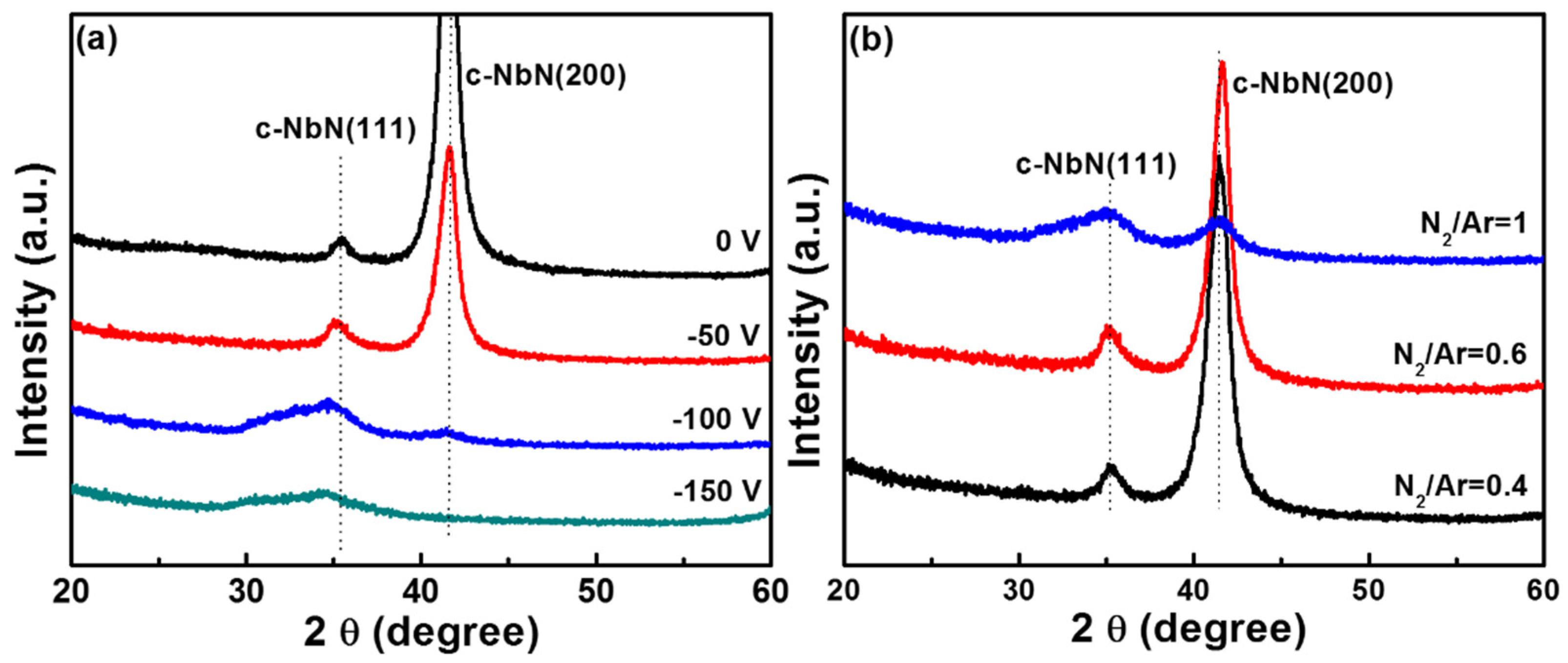
3.1. Elemental Composition and Phase Structure of NbNx>1 Coatings

Figure 1 plots the elemental composition of the NbN coatings as a function of substrate bias and N2/Ar gas ratio measured by EPMA. A relative low oxygen (O) content, i.e., 3 at.%, in all coatings was possibly derived from the residual gas in the vacuum chamber and/or the Nb target that was fabricated by self-propagating high-temperature synthesis. As the bias voltages increased from 0 V to −100 V (Figure 1a), the N content slightly increased from 55.4 at.% to 59.4 at.%, then rebounded to 58.4 at.% at −150 V bias voltage, while the Nb content was almost constant value at around 41 at.%. As to Figure 1b, with increasing N2/Ar gas ratio, the N content also slightly increased. The adequate N reacted with Nb atoms and the superfluous N atoms could squash into the interstitial positions of NbN structure, which finally reached to a saturated value. It was considered that the relatively high N2/Ar gas ratio (over 0.3) leads to the formation of coatings with over N content, which was also found by Benkahoul et al. and Jun et al. [11,24]. The NbNx>1 coatings sputtered under these conditions are all over stoichiometric x = N/Nb > 1. Nitriding is another factor that needs to be considered. In the rotation of the substrate (the substrate does not face the sputtered Nb target for most of rotation time) and/or at a small duty cycle (the time during pulse-off is long compared with the pulse-on time), the coating is additionally nitrided and this results in no dependence of N content on bias voltage and N2/Ar ratio.
Figure 2 shows the XRD patterns of NbNx>1 coatings deposited at different conditions. All the coatings were composed of NbN phase (PDF#710162). As can be seen in Figure 2a, a strong cubic (200) peak appeared in absence of bias NbNx>1 coating, accompanying a weaker cubic (111) peak, which implied that (200) presented a preferred orientation growth. It is ascribed to low energy Ebi delivered to growing coating by bombarding ions. This fact was demonstrated in sputtering of Ti(Al,V)N films, as reported by Jmusil et al. [21]. With increasing bias voltage, the intensity of (200) peaks significantly decreased and vanished at −150 V bias voltage, while the broadening of (111) peak remained. Two phenomena need to be noticed: (1) a slight shift to lower angle was seen in NbNx>1 coatings from XRD pattern, indicating the presence of negative residual stress in these coatings [1]; and (2) the width of peaks become broader with increasing bias voltage, implying grain refinement effect [25]. With increase of bias voltage, the energy of the incident ions not only increase the mobility of the condensing atoms but also result in secondary nuclei and columnar growth being interrupted, which can cause the diminution of grain size and formation of nanocrystals; all these factors are conducive to peak broadening. These results demonstrate that the bias voltage has a major influence on crystal structure change, which means that the change of the NbNx>1 coating structure is caused by increasing Ebi with increasing substrate bias. Figure 2b presents X-ray diffraction patterns of the NbNx>1 coatings deposited with fixed −50 V bias but different N2/Ar gas ratios. The crystalline preferred orientation changed from c-NbNx>1 (200) plane to c-(111) and c-(200) planes co-existing when the N2/Ar gas ratio increased from 0.4 to 1. Similar to the effect of bias voltage, change of gas ratio also caused peak broadening.

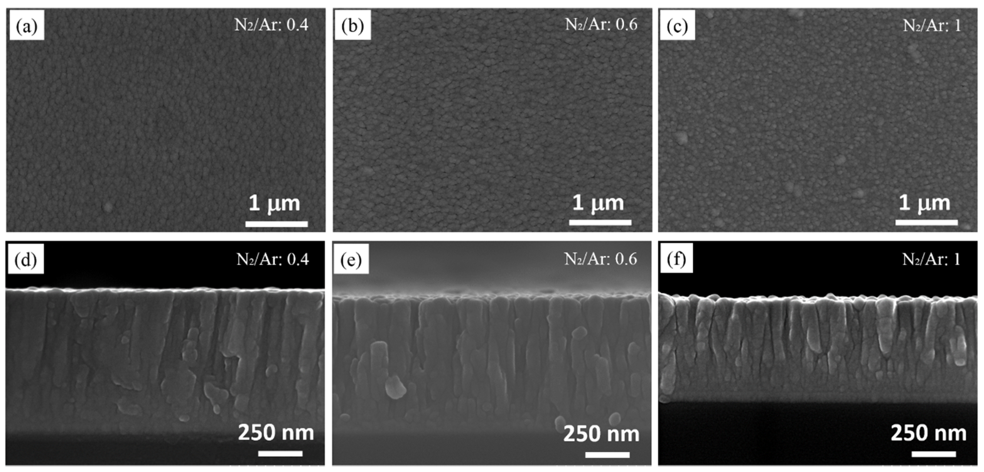
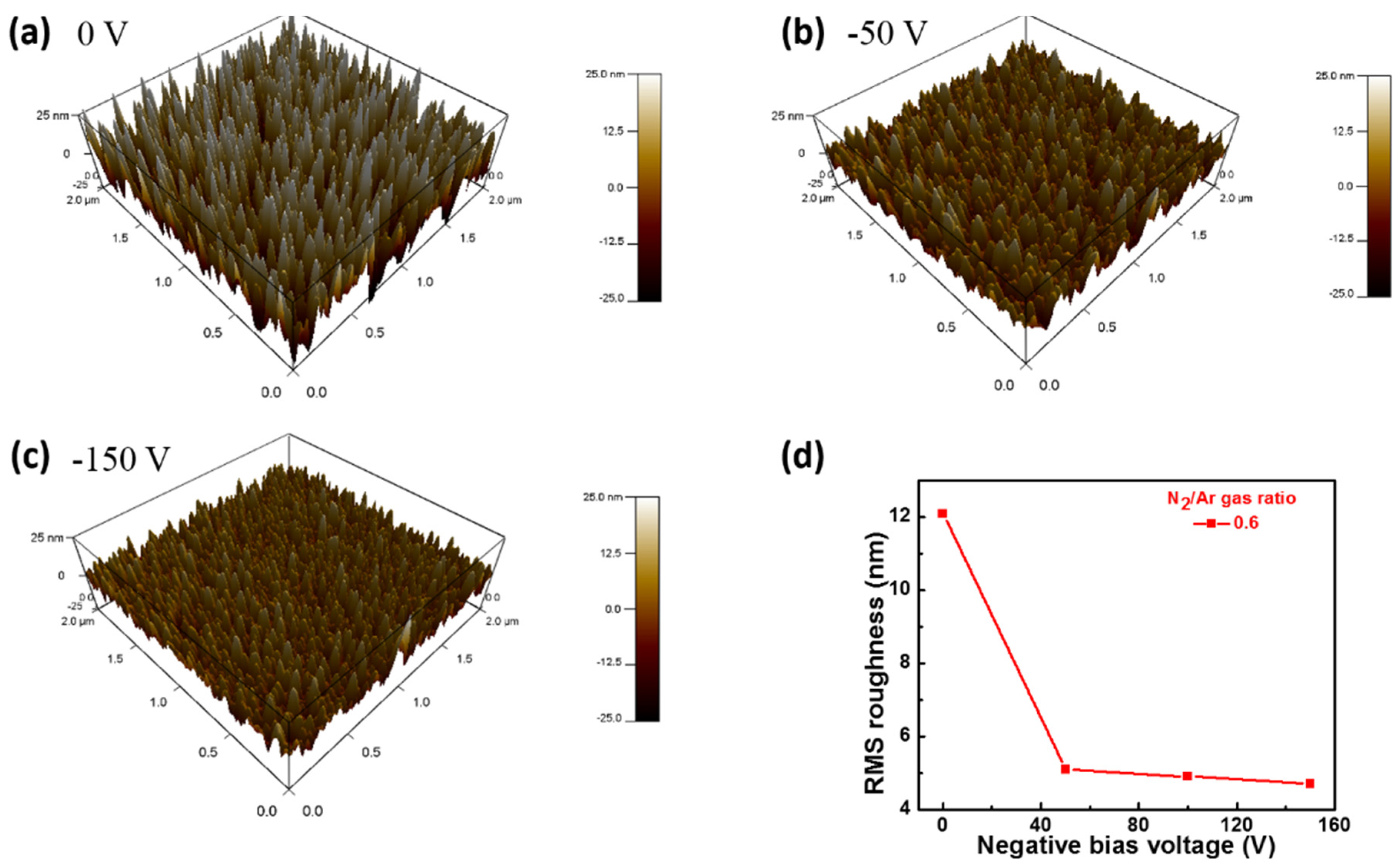
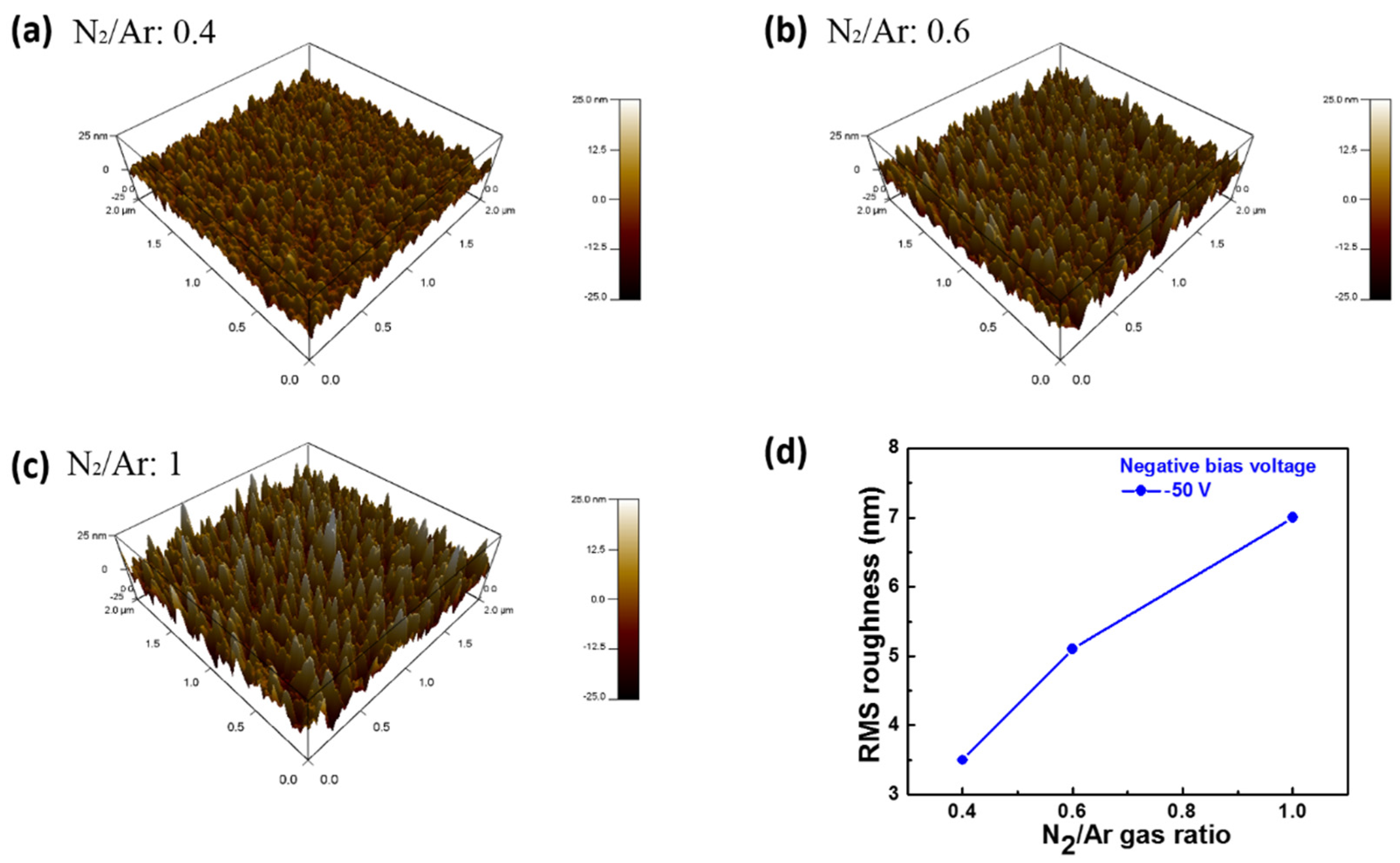
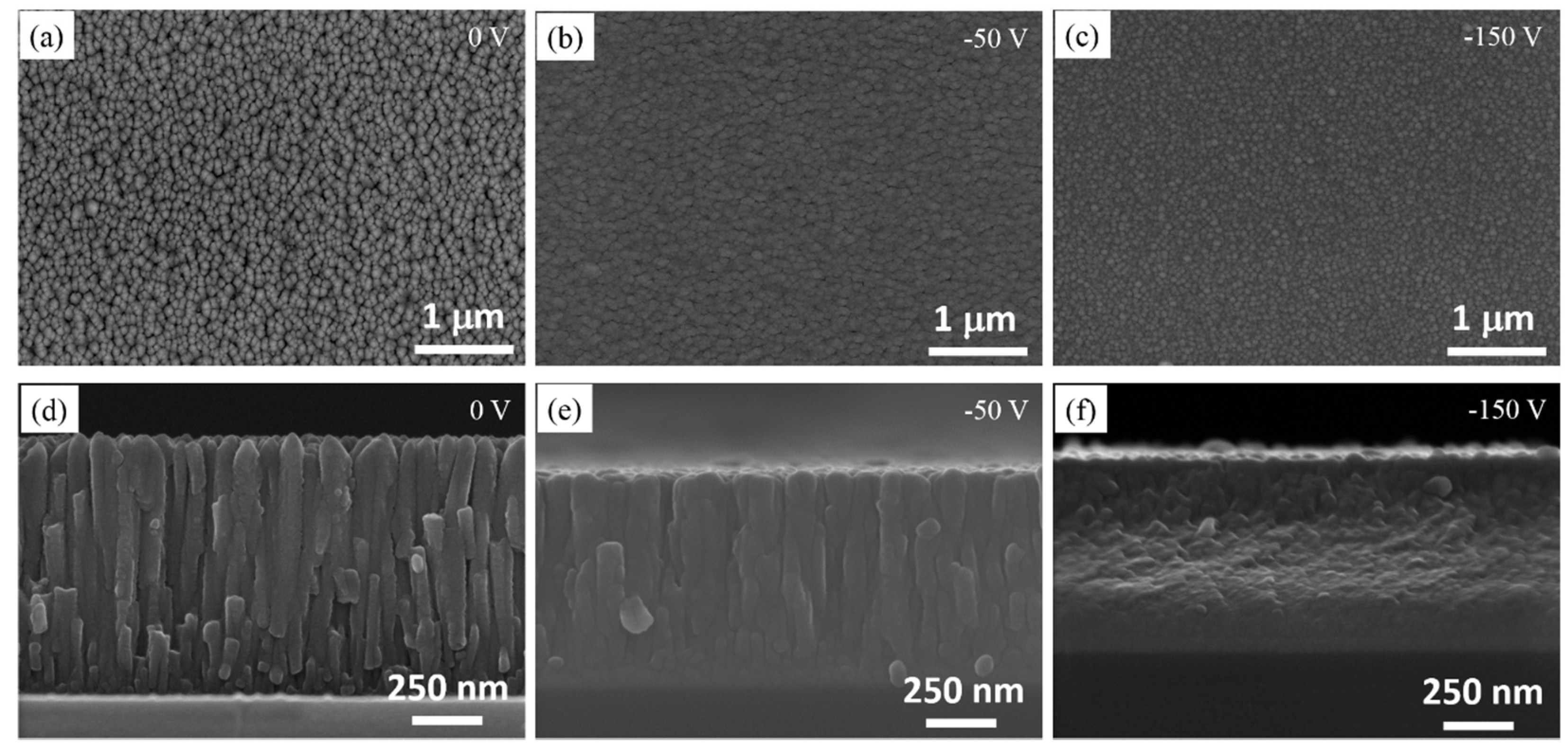
3.2. Microstructure and Surface Topographies of NbNx>1 Coatings

To investigate the microstructure and surface topographies of NbNx>1 coatings, the SEM and AFM investigations were conducted on typical samples. Figure 3 shows the surface images and the corresponding fractured cross-sectional SEM images of the NbNx>1 coatings deposited at various bias voltages, viz. 0, −50, and −150 V, when N2/Ar gas ratio was fixed to 0.6. In Figure 3a, without bias voltage, the coating exhibited circular rods that were loosely lined up on the surface. The corresponding cross-section image, as shown in Figure 3d, has pronounced columnar units with visible gap grow outward from the film-interlayer interface and throughout the whole film thickness. With applying bias voltage from −50 to −150 V, as shown in Figure 3b,c, the granular size on the surface decreased and became more compact. At −50 V low bias voltage condition, the prominent columnar structure still existed in Figure 3e, and was much denser than in Figure 3d. When the bias voltage increased to −150 V, the pronounced columnar structure was almost invisible so that the fracture cross-section was nearly featureless, in accordance with previous results [26,27]. It was considered that as the bias voltage increased, the increased energy delivered to the surface adatom, which could effectively increase the surface adatom mobility. This movement would fill the voids between the grains, break down the large columnar grain growth, and create more nucleation sites, thereby increasing the density of the coatings and promoting the grain refinement. The result of grain refinement is also in agreement with XRD pattern, as mentioned in Figure 2a. It is noted that the thickness is decreased with increasing bias voltage from Figure 3d–f. Two possible reasons could explain this observation. One is that enhanced incident ions energy could lead to the microstructure changing from loose to denser; and the other is that more atoms from the growing coatings could re-sputter at a higher bias voltage. Therefore, it is assumed that the change of microstructure and the re-sputtering are responsible for this phenomenon in the present study. However, at the same −50 V bias voltage and various N2/Ar gas ratios, all the granules were compact except those randomly distributed particles which were slightly increased at the surface of coatings, as shown in Figure 4a–c. These coatings also exhibited apparent columnar structure, nevertheless, the thickness dramatically decreased with increase of N2/Ar gas ratio, as shown in Figure 4d–f. Similarly, Singh et al. [10] and Wang et al. [28] ascribed it to the well-known target-poisoning, namely, the emitting atoms and ions from the Nb target were greatly decreased due to the partial covering of high melting-point NbN on the Nb target surface. However, the reason of target-poisoning does not meet the practical situation in this study as the average voltage/current almost was constant in the whole sputtering process, suggesting that target poisoning effects in the sputtering process were absent. The reason for this decrease in the thickness is the poor sputtering ability of nitrogen compared to argon [29]. This result also shows that HiPIMS deposition possesses high gas ionization rate and can effectively avoid target poisoning effect.
Figure 5 shows the typical surface topographies and roughness of the NbNx>1 coatings deposited at different bias voltages. At 0 V bias voltage, the obtained topography shown in Figure 5a confirmed that the NbNx>1 coating was composed of small column hillocks, the roughness value was maximum arriving at 12.1 nm. With increasing bias voltage, the roughness value decreased to 5 nm and the minimum roughness of 4.7 nm was obtained at the −150 V bias voltage, as shown in Figure 5c. The surface roughness evolution of coatings could be explained by the bias effect, which also were in good agreement with earlier reports on different hard coatings [28,30]. With increasing bias voltage, the mobility of the impinging ions and adatoms are increase, which eventually favors the formation of a dense coatings and surfaces of lower roughness. Comparing Figure 6 to Figure 5, it is found that the surface roughness of NbNx>1 coatings increased with the increase of N2/Ar gas ratio. The mean free path (λ) of these molecule/ions differ between the nitrogen and argon, and the λ shown as following formula [31]:
λ = k T 2 π σ 2 p  
where k is Boltzmann constant, T is Kelvin degree, σ is the effective diameter of molecule or ion, and p is the pressure in the chamber. It is known that the N2 gas has a larger molecular diameter is than Ar gas and the mean free path becomes smaller with increase of N2 gas partial pressure. It may suffer from much collisions and the injection energy to the surface of coatings will become lower. Thus, it will decrease bombardment effects of the injected particles and will cause poor surface diffusion, resulting in coarse surface compared to lower N2 partial pressure. Another explanation on the variation of roughness: as shown in Figure 4a, the surface of coatings was much smoother than the surface of high N2/Ar ratio coating. Figure 4d–f shows that the columnar structure was very compact and dense in N2/Ar ratio of 0.4, whereas, with increasing values of N2/Ar ratio, the columnar structure became coarser and looser, which were contributed to the enhancement of surface roughness.

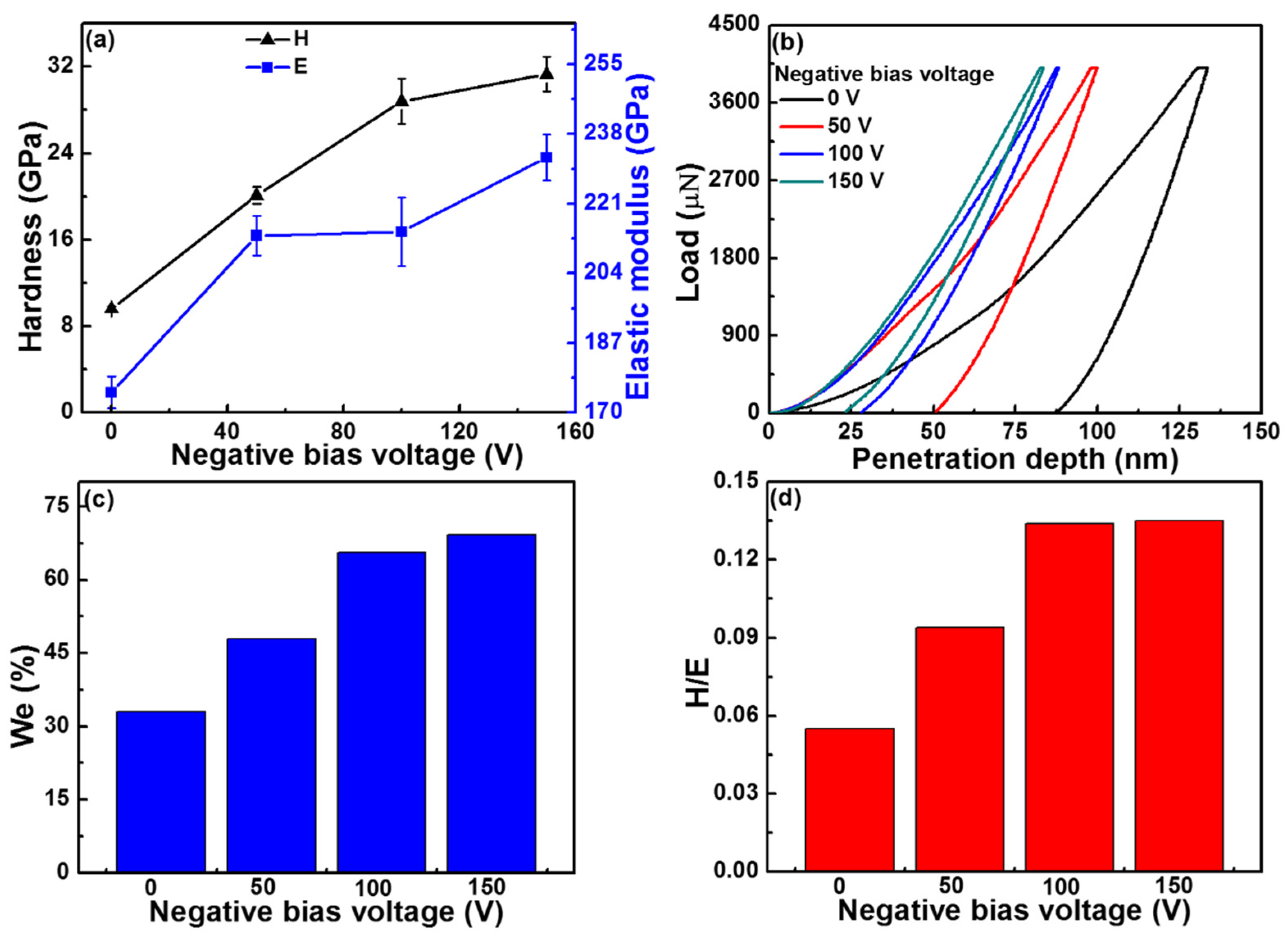
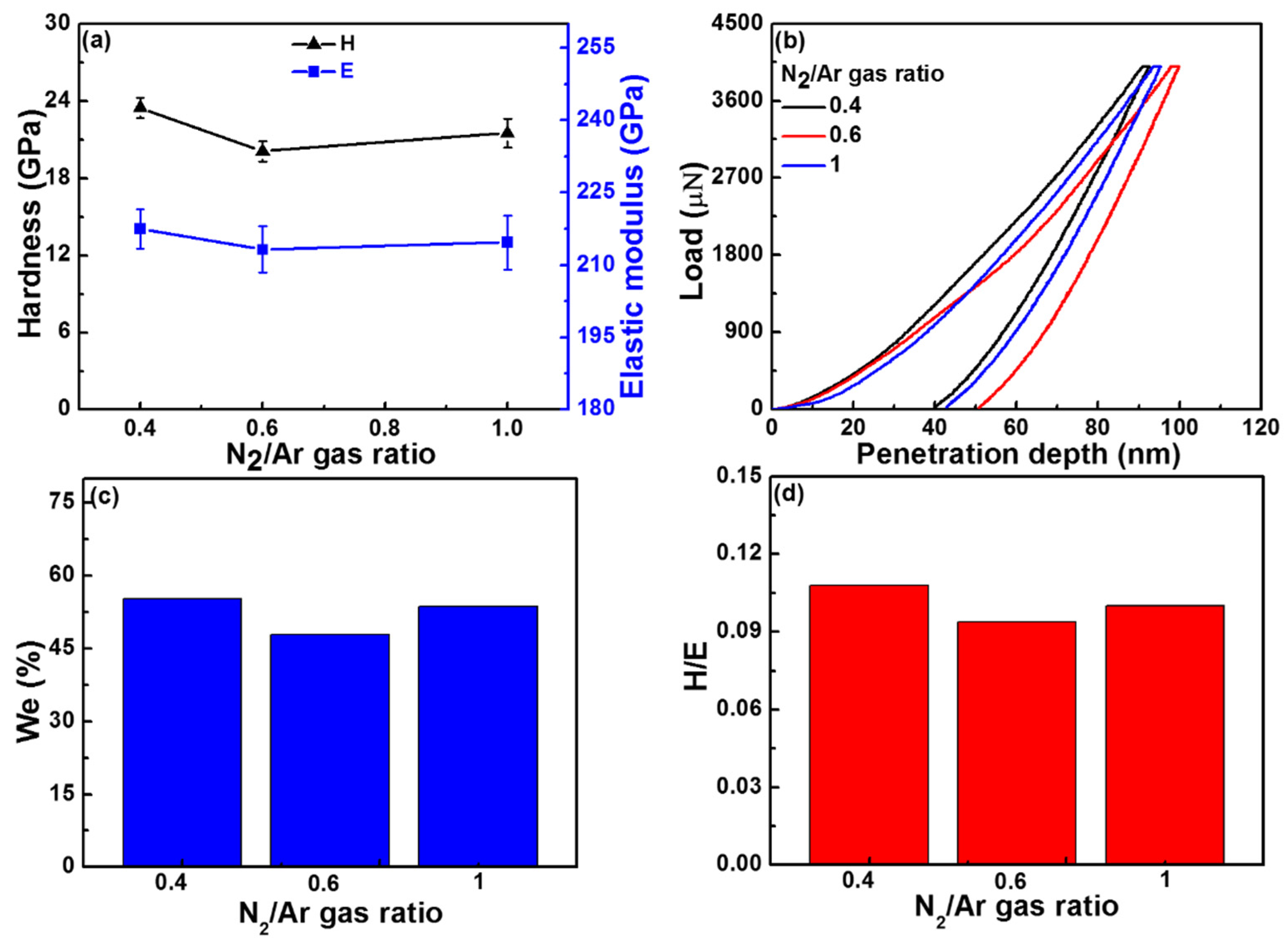
3.3. Mechanical Properties of NbNx>1 Coatings

To minimize the effect of substrate and coating thickness, nanoindentation tests were performed to evaluate coating hardness, and the penetration depth was adopted to less than 15% (10%–15%) of coating thickness. A total of ten indentations were tested on each sample and the mean values and standard deviation was computed. Figure 7 presents the hardness H, elastic modulus E, typical load–displacement curves, elastic recovery We and H/E ratio of the coatings versus various bias voltages. With increasing the bias voltage, the coating hardness gradually increased from 9.6 to 31.3 GPa. Correspondingly, the elastic modulus increases from 175 to 232.3 GPa. As usual that, the coating with a higher hardness exhibits a higher elastic modulus. The trend was in agreement with Pogrebnjak et al. [32], who reported an increase of bias voltage leads to increasing H and E in NbN films, and the maximum hardness (28 GPa) is obtained at −70 V bias voltage. The hardness enhancement in the coatings could be attributed to grain size refinement and microstructure change. As discussed before, the grain refinement and change of microstructure were verified with increasing bias voltage. Smaller grains increased the effect of dislocation blocking and thereby strengthen the material. At high bias, the microstructure changed from porous to dense, which is also beneficial to enhance hardness. Some other minor effects induced by bias; e.g., residual stress might also contribute to part of the hardness improvement. Both the coating hardness and elastic modulus have been proposed to play a key roles in determining the wear and cracking resistances of the hard coatings. In particular, the ratio of the coating hardness over the elastic modulus H/E was used as a more suitable parameter for predicting the wear and cracking resistance compared to hardness alone [33]. Figure 7c,d shows the elastic recovery We and H/E ratio of the NbNx>1 coatings. Musil. et al. [34] demonstrated the need of high value of the We for the reduction of friction and wear of the hard coatings. In Figure 7c, the We increased from 33% for NbNx>1 without bias voltage to 69.2% at −150 V bias voltage. The enhanced We supported for an improvement of the resistance to the friction and wear. In Figure 7d, the H/E ratio of the coatings increased from 0.055 to 0.135 corresponding with increasing the bias voltage from 0 to −150 V. Thus, the NbNx>1 coating with H/E ≥ 0.1 and We ≥ 60% and dense voids-free microstructure exhibiting an enhanced resistance to cracking and wear was deduced [35]. For the coatings deposited at different N2/Ar gas ratios, as shown in Figure 8, the hardness and elastic modulus were changed from 23.5 and 217.5 GPa to 21.5 and 214.7 GPa, respectively. The difference in surface roughness might be responsible for the slight decrease in hardness. Same tendency in elastic recovery and H/E ratio is seen in Figure 8c,d. The value of H/E ratio was around at 0.1, implying that these coatings possessed comparative properties of resistance to wear. However, when compared with that of the bias voltage, due to the less variation in microstructure with various N2/Ar gas ratios, the effect of N2/Ar gas ratios on mechanical properties are less notable.

4. Conclusions

Pure NbNx>1 coatings have been prepared successfully using HiPIMS deposition system under various negative bias voltages and N2/Ar gas ratios. The XRD patterns, microstructure and mechanical properties of the coatings are investigated systemically. The following main conclusions were obtained.
  • The stoichiometry x of NbNx does not depend on the negative substrate bias or the N2/Ar ratio. All sputtered NbNx coatings are over stoichiometric with x = N/Nb > 1. It is the result of an additional nitriding of growing coating during the substrate rotation or the pulse-off time between pulses in the HiPIMS process. The preferred orientation of NbNx>1 coating changes from (200) to (111) with increasing bias voltage, i.e., with increasing energy Ebi delivered into the coating by bombarding ions. The hardness H and elastic recovery We increases with increasing negative substrate bias voltage due to increasing energy Ebi. The NbNx>1 coatings sputtered at negative substrate bias over −100 V exhibit high values of H/E > 0.1 and We > 60% and dense, void-free microstructure.
  • Increasing N2/Ar gas ratio has resulted in the change of NbNx>1 preferred orientations from (200) phase to (200) and (111) coexisting phases. The grain refinement is also found in these coatings. Due to the poor sputtering capability of nitrogen compared with argon, the thickness of NbNx>1 coatings is vastly decreased and the roughness value is increased with increasing the ratio of N2/Ar gas. However, the N2/Ar gas ratio showed little effect on mechanical properties of the coatings, which is ascribed to the less variation in microstructure with various N2/Ar gas ratios in the coatings.
  • The obtained coatings deposited by HiPIMS method show smooth surfaces and superior mechanical properties compared to DC sputtering, which indicated the merits of HiPIMS technique for industrial applications.

Acknowledgments

This work was supported by the Global Frontier Program through the Global Frontier Hybrid Interface Materials (GFHIM) of the National Research Foundation of Korea (NRF) funded by the Ministry of Science, ICT & Future Planning (2013M3A6B1078874). In addition, the authors also acknowledge the financial supports of the NSFC project (51522502) and Guangdong Natural Science Fund (2016A050502056).

Author Contributions

Jicheng Ding designed the study, carried out PVD deposition, analyzed the experiment data, and drafted the manuscript. Tengfei Zhang revised and reconstruction of the data in the manuscript. Haijuan Mei and Je Moon Yun performed the investigation of samples (EPMA, SEM, AFM). Seong Hee Jeong did the hardness investigation. Qimin Wang and Kwang Ho Kim conceived the study, participated in its design, and supervised the manuscript. All authors have read and approved the final manuscript.

Conflicts of Interest

The authors declare no conflict of interest.

References

  1. Ding, J.C.; Zhang, T.F.; Yun, J.M.; Kang, M.C.; Wang, Q.M.; Kim, K.H. Microstructure, Mechanical, Oxidation and Corrosion properties of the Cr–Al–Si–N coatings deposited by a hybrid sputtering system. Coatings 2017, 7, 119. [Google Scholar] [CrossRef]
  2. Tian, C.X.; Yang, B.; He, J.; Wang, H.J.; Fu, D.J. Structure and mechanical properties of CrNx coatings deposited by Medium-Frequency Magnetron Sputtering with and without Ion Source Assistance. J. Nanomater. 2011, 201, 534647. [Google Scholar]
  3. Sabitzer, C.; Paulitsch, J.; Kolozsvári, S.; Rachbauer, R.; Mayrhofer, P.H. Impact of bias potential and layer arrangement on thermal stability of arc evaporated Al–Cr–N coatings. Thin Solid Films 2016, 610, 26–34. [Google Scholar] [CrossRef]
  4. Lu, L.; Wang, Q.M.; Chen, B.Z.; Ao, Y.C.; Yu, D.H.; Wang, C.Y.; Wu, S.H.; Kim, K.H. Microstructure and cutting performance of CrTiAlN coating for high-speed dry milling. Trans. Nonferr. Met. Soc. China 2014, 24, 1800–1806. [Google Scholar] [CrossRef]
  5. Liu, W.; Li, A.Q.; Wu, H.D.; He, R.X.; Huang, J.W.; Long, Y.; Deng, X.; Wang, Q.M.; Wang, C.Y.; Wu, S.H. Effects of bias voltage on microstructure, mechanical properties, and wear mechanism of novel quaternary (Ti, Al, Zr)N coating on the surface of silicon nitride ceramic cutting tool. Ceram. Int. 2016, 42, 17693–17697. [Google Scholar] [CrossRef]
  6. Kim, S.K.; Cha, B.C.; Yoo, J.S. Deposition of NbN thin films by DC magnetron sputtering process. Surf. Coat. Technol. 2004, 177–178, 434–440. [Google Scholar] [CrossRef]
  7. Singh, K.; Bidaye, A.C.; Suri, A.K. Magnetron sputtered NbN films with electroplated Cr interlayer. Vacuum 2011, 86, 267–274. [Google Scholar] [CrossRef]
  8. Wen, M.; Hu, C.Q.; Wang, C.; An, T.; Su, Y.D.; Meng, Q.N. Effects of substrate bias on the preferred orientation, phase transition and mechanical properties for NbN films grown by direct current reactive magnetron sputtering. J. Appl. Phys. 2008, 104, 023527. [Google Scholar] [CrossRef]
  9. Sandu, C.S.; Benkahoul, M.; Wojtan, M.P.; Sanjines, R.; Levy, F. Morphological, structural and mechanical properties of NbN thin films deposited by reactive magnetron sputtering. Surf. Coat. Technol. 2006, 200, 6544–6548. [Google Scholar] [CrossRef]
  10. Singh, K.; Bidaye, A.C.; Suri, A.K. Magnetron sputtered NbN films with Nb interlayer on mild steel. Int. J. Corros. 2011, 2011, 748168. [Google Scholar] [CrossRef]
  11. Benkahoul, M.; Martinez, E.; Karimi, A.; Sanjines, R.; Levy, F. Structural and mechanical properties of sputtered cubic and hexagonal NbNx thin films. Surf. Coat. Technol. 2004, 180–181, 178–183. [Google Scholar] [CrossRef]
  12. Cappuccio, G.; Gambardella, U.; Morone, A.; Orlando, S.; Parisi, G. Pulsed laser ablation of NbN/Mgo/NbN multilayers. Appl. Surf. Sci. 1997, 109–110, 399–402. [Google Scholar] [CrossRef]
  13. Hayashi, N.; Murzin, I.H.; Sakamoto, I.; Ohkubo, M. Single-crystal niobium nitride thin films prepared with radical beam assisted deposition. Thin Solid Films 1995, 259, 146–149. [Google Scholar] [CrossRef]
  14. Bendavid, A.; Martin, P.J.; Kinder, T.J.; Preston, E.W. The deposition of NbN and NbC thin films by filtered vacuum cathodic arc deposition. Surf. Coat. Technol. 2003, 163–164, 347–352. [Google Scholar] [CrossRef]
  15. Cansever, N. Properties of niobium nitride coatings deposited by cathodic arc physical vapor deposition. Thin Solid Films 2007, 515, 3670–3674. [Google Scholar] [CrossRef]
  16. Kim, D.H.; Zhang, T.F.; Shin, J.H.; Kang, M.C.; Kim, K.H. Microstructure and mechanical properties of Cr–Ni–N coatings deposited by HIPIMS. Surf. Eng. 2016, 32, 314–320. [Google Scholar] [CrossRef]
  17. Sarakinos, K.; Alami, J.; Konstantinidis, S. High power pulsed magnetron sputtering: A review on scientific and engineering state of the art. Surf. Coat. Technol. 2010, 204, 1661–1684. [Google Scholar] [CrossRef]
  18. Giudice, L.D.; Adjam, S.; Grange, D.L.; Banakh, O.; Karimi, A.; Sanjines, R. NbTiN thin films deposited by hybrid HiPIMS/DC magnetron co-sputtering. Surf. Coat. Technol. 2016, 295, 99–106. [Google Scholar] [CrossRef]
  19. Paulitsch, J.; Schenkel, M.; Zufrab, T.; Mayrhofer, P.H.; Munz, W.D. Structure and properties of high power impulse magnetron sputtering and DC magnetron sputtering CrN and TiN films deposited in an industrial scale unit. Thin Solid Films 2010, 518, 5558–5564. [Google Scholar] [CrossRef]
  20. Ehiasarian, A.P.; Hovsepian, P.E.; Hultman, L.; Helmersson, U. Comparison of microstructure and mechanical properties of chromium nitride-based coatings deposited by high power impulse magnetron sputtering and by the combined steered cathodic arc/unbalanced magnetron technique. Thin Solid Films 2004, 457, 270–277. [Google Scholar] [CrossRef]
  21. Musil, J.; Jaros, M.; Cerstvy, R.; Haviar, S. Evolution of microstructure and macrostress in sputtered hard Ti(Al,V)N films with increasing energy delivered during their growth by bombarding ions. J. Vac. Sci. Technol. A 2017, 35. [Google Scholar] [CrossRef]
  22. Musil, J. Flexible hard nanocomposite coatings. RSC Adv. 2015, 5, 60482–60495. [Google Scholar] [CrossRef]
  23. Pharr, G.M. Measurement of mechanical properties by ultra-low load indentation. Mater. Sci. Eng. A 1998, 253, 151–159. [Google Scholar] [CrossRef]
  24. Jun, S.H.; Kim, J.H.; Kim, S.K.; You, Y.Z.; Cha, B.C. Characteristics of NbN films deposited on AISI 304 using inductively coupled plasma assisted DC magnetron sputtering method. J. Korean Inst. Surf. Eng. 2013, 46, 187–191. [Google Scholar] [CrossRef]
  25. Lin, J.; Sproul, W.D.; Moore, J.J.; Wu, Z.L.; Lee, S.L. Effect of negative substrate bias voltage on the structure and properties of CrN films deposited by modulated pulsed power (MPP) magnetron sputtering. J. Phys. D Appl. Phys. 2011, 44, 425305. [Google Scholar] [CrossRef]
  26. Zhang, M.; Li, M.K.; Kim, K.H.; Pan, F. Structural and mechanical properties of compositionally gradient CrNx coatings prepared by arc ion plating. Appl. Surf. Sci. 2009, 255, 9200–9205. [Google Scholar] [CrossRef]
  27. Tan, S.Y.; Zhang, X.H.; Zhang, Y.; Zhen, R.; Zhu, X.F.; Tian, Z.; Wang, Z.Z. Microstructure and properties of Cr–Cu–N coatings with ultra-low copper content. Surf. Coat. Technol. 2015, 275, 270–275. [Google Scholar] [CrossRef]
  28. Wang, Q.M.; Kim, K.H. Effect of negative bias voltage on CrN films deposited by arc ion plating. I. Macroparticles filtration and film-growth characteristics. J. Vac. Sci. Technol. A 2008, 26, 1258–1266. [Google Scholar] [CrossRef]
  29. Zhang, G.A.; Yan, P.X.; Wang, P.; Chen, Y.M.; Zhang, J.Y. Influence of nitrogen content on the structural, electrical and mechanical properties of CrNx thin films. Mater. Sci. Eng. A 2007, 460–461, 301–305. [Google Scholar] [CrossRef]
  30. Kong, Q.H.; Ji, L.; Li, H.X.; Liu, X.H.; Wang, Y.J.; Chen, J.M.; Zhou, H.D. Influence of substrate bias voltage on the microstructure and residual stress of CrN films deposited by medium frequency magnetron sputtering. Mater. Sci. Eng. B 2011, 176, 850–854. [Google Scholar] [CrossRef]
  31. Neidhardt, J.; Mráz, S.; Schneider, J.M.; Strub, E.; Bohne, W.; Liedke, B.; Möller, W.; Mitterer, C. Experiment and simulation of the compositional evolution of Ti–B thin films deposited by sputtering of a compound target. J. Appl. Phys. 2008, 104, 063304. [Google Scholar] [CrossRef]
  32. Pogrebnjak, A.D.; Bondar, O.V.; Abadias, G.; Ivashchenko, V.; Sobol, O.V.; Jurga, S.; Coy, E. Structural and mechanical properties of NbN and Nb–Si–N films: Experiment and molecular dynamics simulations. Ceram. Int. 2016, 42, 11743–11756. [Google Scholar] [CrossRef]
  33. Leyland, A.; Matthews, A. On the significance of the H/E ratio in wear control: a nanocomposite coating approach to optimized tribological behavior. Wear 2000, 246. [Google Scholar] [CrossRef]
  34. Musil, J.; Kunc, F.; Zeman, H.; Polakova, H. Relationships between hardness, Young’s modulus and elastic recovery in hard nanocomposite coatings. Surf. Coat. Technol. 2002, 154, 304–313. [Google Scholar] [CrossRef]
  35. Musil, J. Hard nanocomposite coatings: Thermal stability, Oxidation resistance and toughness. Surf. Coat. Technol. 2012, 207, 50–65. [Google Scholar] [CrossRef]
Figure 1. Elemental compositions of NbN coatings deposited under different bias voltages with constant 0.6 ratio of N2/Ar (a); and under different N2/Ar gas ratios with constant −50 V bias voltage (b).
Coatings 08 00010 g001
Figure 2. XRD patterns of NbNx>1 coatings deposited under different bias voltages with constant 0.6 ratio of N2/Ar (a); and under different N2/Ar gas ratios with constant −50 V bias voltage (b).
Coatings 08 00010 g002
Figure 3. Surface (ac) and cross-sectional images (df) of NbNx>1 coatings deposited under different bias voltages with constant 0.6 ratio of N2/Ar.
Coatings 08 00010 g003
Figure 4. Surface (ac) and cross-sectional images (df) of NbNx>1 coatings deposited at different N2/Ar gas ratios with constant −50 V bias voltage.
Coatings 08 00010 g004
Figure 5. The three-dimensional topographic AFM images of the typical NbNx>1 samples (ac), and Root Mean Square (RMS) roughness deposited under different bias voltages with constant 0.6 ratio of N2/Ar (d).
Coatings 08 00010 g005
Figure 6. The three-dimensional topographic AFM images of the typical NbNx>1 samples (ac), and Root Mean Square (RMS) roughness deposited at different N2/Ar gas ratios with constant −50 V bias voltage (d).
Coatings 08 00010 g006
Figure 7. Hardness (H) and elastic modulus (E) (a); load-displacement curves (b); elastic recovery (We) (c); and H/E value of NbNx>1 coatings deposited under different bias voltages with constant 0.6 ratio of N2/Ar (d).
Coatings 08 00010 g007
Figure 8. Hardness (H) and elastic modulus (E) (a); load-displacement curves (b); elastic recovery (We) (c) and H/E value of NbNx>1 coatings deposited at different N2/Ar gas ratios with constant −50 V bias voltage (d).
Coatings 08 00010 g008
Table 1. The HiPIMS pulsing parameters and deposition conditions for NbN coatings.
ParametersValue
Pulse ParametersRepetition Frequency147 Hz
Duty Cycle14%
Pa0.8 kW
Pp14 kW
Wt16 W/cm2
Base Pressure5 × 10−3 Pa
Working Pressure0.5 Pa
Substrate temperature300 °C
Substrate to target distance120 mm
Deposition time150 min
Table 2. The thickness and Ebi of NbN coatings as a function of bias voltage.
N2/Ar RatioBias Voltage (V)Ebi (MJ/cm3)Thickness (nm)
0.6001000
0.6−501.42890
0.6−1004.18796
0.6−1508.75709
Table 3. The thickness of NbN coatings as a function of N2/Ar ratio.
Bias Voltage (V)N2/Ar RatioThickness (nm)
−500.4900
−500.6890
−501612

