Article

Strain Effects by Surface Oxidation of Cu3N Thin Films Deposited by DC Magnetron Sputtering

1
Institute of Physics, University of Greifswald, Felix Hausdorff Str. 6, Greifswald 17489, Germany
2
Indian Institute of Engineering Science and Technology, Shibpur, Howrah-3, West Bengal 711103, India
3
Surface Physics & Materials Science Division, Saha Institute of Nuclear Physics, 1/AF Bidhan Nagar, Kolkata 700 064, India
*
Author to whom correspondence should be addressed.
Coatings 2017, 7(5), 64; https://doi.org/10.3390/coatings7050064
Submission received: 2 December 2016 / Revised: 21 April 2017 / Accepted: 26 April 2017 / Published: 29 April 2017

Abstract

:
We report the self-buckling (or peeling off) of cubic Cu3N films deposited by DC magnetron sputtering of a Cu target in a nitrogen environment at a gas pressure of 1 Pa. The deposited layer partially peels off as it is exposed to ambient air at atmospheric pressure, but still adheres to the substrate. The chemical composition of the thin film as investigated by means of X-ray photoelectron spectroscopy (XPS) shows a considerable surface oxidation after exposure to ambient air. Grazing incidence X-ray diffraction (GIXRD) confirms the formation of a crystalline Cu3N phase of the quenched film. Notable are the peak shifts in the deposited film to smaller angles in comparison to stress-free reference material. The X-ray pattern of Cu3N exhibits clear differences in the integral width of the line profiles. Changes in the film microstructure are revealed by X-ray diffraction, making use of X-ray line broadening (Williamson–Hall and Stokes–Fourier/Warren–Averbach method); it indicates that the crystallites are anisotropic in shape and show remarkable stress and micro-strain.

1. Introduction

The interest in copper nitride (Cu3N) thin films has increased in recent years due to their potential applications for recording media [1,2,3] and as precursor material for microscopic copper lines by mask-less laser writing [4]. Various methods have been employed to obtain copper nitride films, such as RF-sputtering [5,6,7,8,9], RF-plasma chemical reactor [10], reactive pulsed laser deposition [11], and activated reactive evaporation [12]. Despite the promising properties of Cu3N, large discrepancies reported in the literature about its measured physical properties have hampered the implementation of reliable technological devices.
The control of the structure and properties of copper nitride films is an interesting topic. In the present work, buckling of the deposited Cu3N film after exposure to ambient air is observed. The deposited thin copper nitride films partially peel off from the silicon substrate within several minutes of air exposure. The crystalline structure and the surface oxidation of the deposited films are investigated and analysed.

2. Materials and Methods

Copper nitride films were prepared by DC magnetron sputtering [13,14,15,16]. The 2″ sputter target was made of oxygen-free copper with a purity of 99.9%. Films were deposited on commercially available p-Si (100) substrates. Alternatively, glass substrates were employed. All substrates were ultrasonically cleaned in acetone. The vacuum chamber was evacuated by a turbo molecular pump to a base pressure of less than 10−5 Pa. The working gas was 99.999% pure N2. The chamber pressure during magnetron operation was maintained at 1 Pa. Typical discharge power during sputter deposition was 100–130 W (discharge voltage 325 V, plasma current 0.4 A). Deposition took place at room temperature and with electrically floating substrates. Films were deposited for 30 min (glass substrate) or 60 min (Si substrate). After deposition, the substrates were taken out of the chamber. The films were further examined using a scanning electron microscope (SEM). The SEM (FEI Company, Hillsboro, OR, USA, Quanta 200F) was operated with an energy of 10 keV at tilt angles of 0.6° and 30° and with typical magnifications of 100.
Film thickness was investigated with the help of spectroscopic ellipsometry employing a phase-modulated ellipsometer (HORIBA Jobin-Yvon Inc., Edison, NJ, USA, UVISEL). The investigated wavelength region was 380–830 nm with energy steps of less than 0.5 nm. The experiments were carried out under an incidence angle of 70° corresponding to the Brewster angle of the Si (100) substrate. A film thickness of 3 μm was derived for the Cu3N/Si film (deposition time 60 min).
Grazing incidence X-ray diffraction (GIXRD, asymmetric Bragg case) measurements were done to determine the phase composition of deposited films; the employed methods are described in Reference [17]. All measurements were performed with a θ–2θ Diffractometer (D5000, Bruker AXS GmbH, Karlsruhe, Germany) using Cu Kα radiation (40 kV, 40 mA). The scanned 2θ range was 20°–50° at a constant incidence angle ω = 1.0°. The crystal structure data of Cu3N were used to identify the crystallographic phases [18].
X-ray photoelectron spectroscopy (XPS) measurements of the Cu3N films were performed on a multi-technique 100 mm hemispherical electron analyser (Fisons Instruments VG Microtech, Uckfield, UK, CLAM2), using Mg Kα radiation (photon energy 1253.6 eV) as the excitation source and the binding energy (BE) of Au (Au 4f7/2: 84.00 eV) as the reference. XPS measurements were performed at two different detector angles of 90° and 20° with respect to the substrate [17].

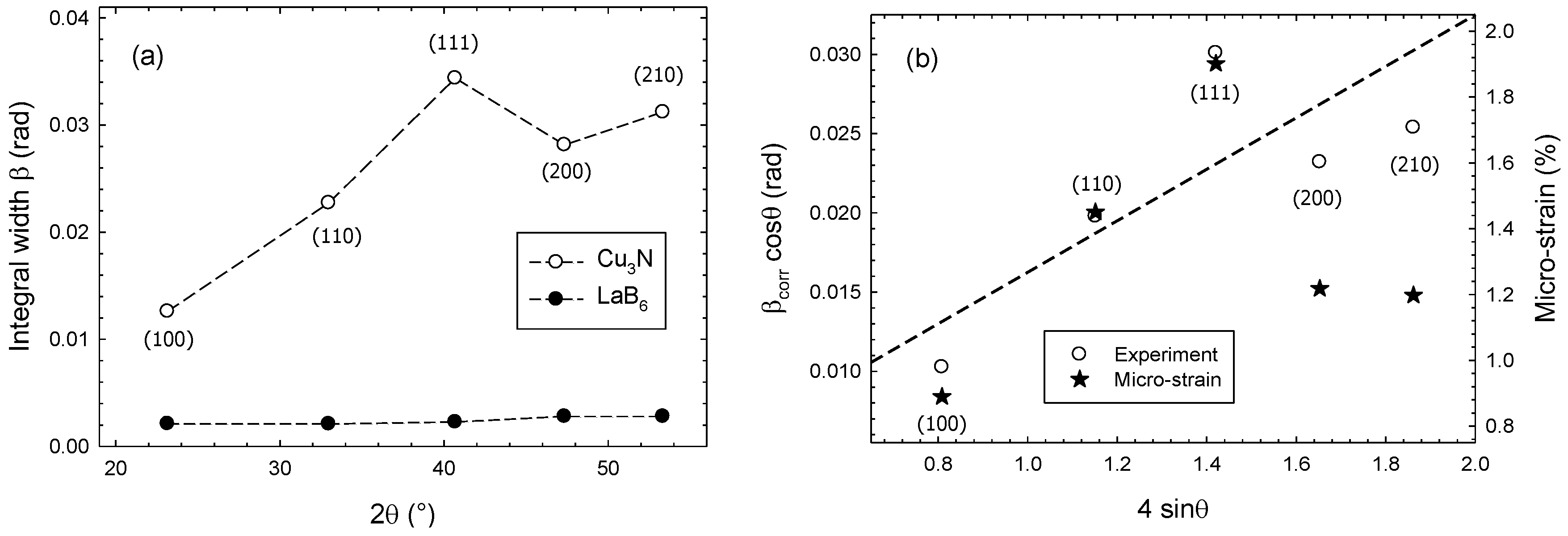
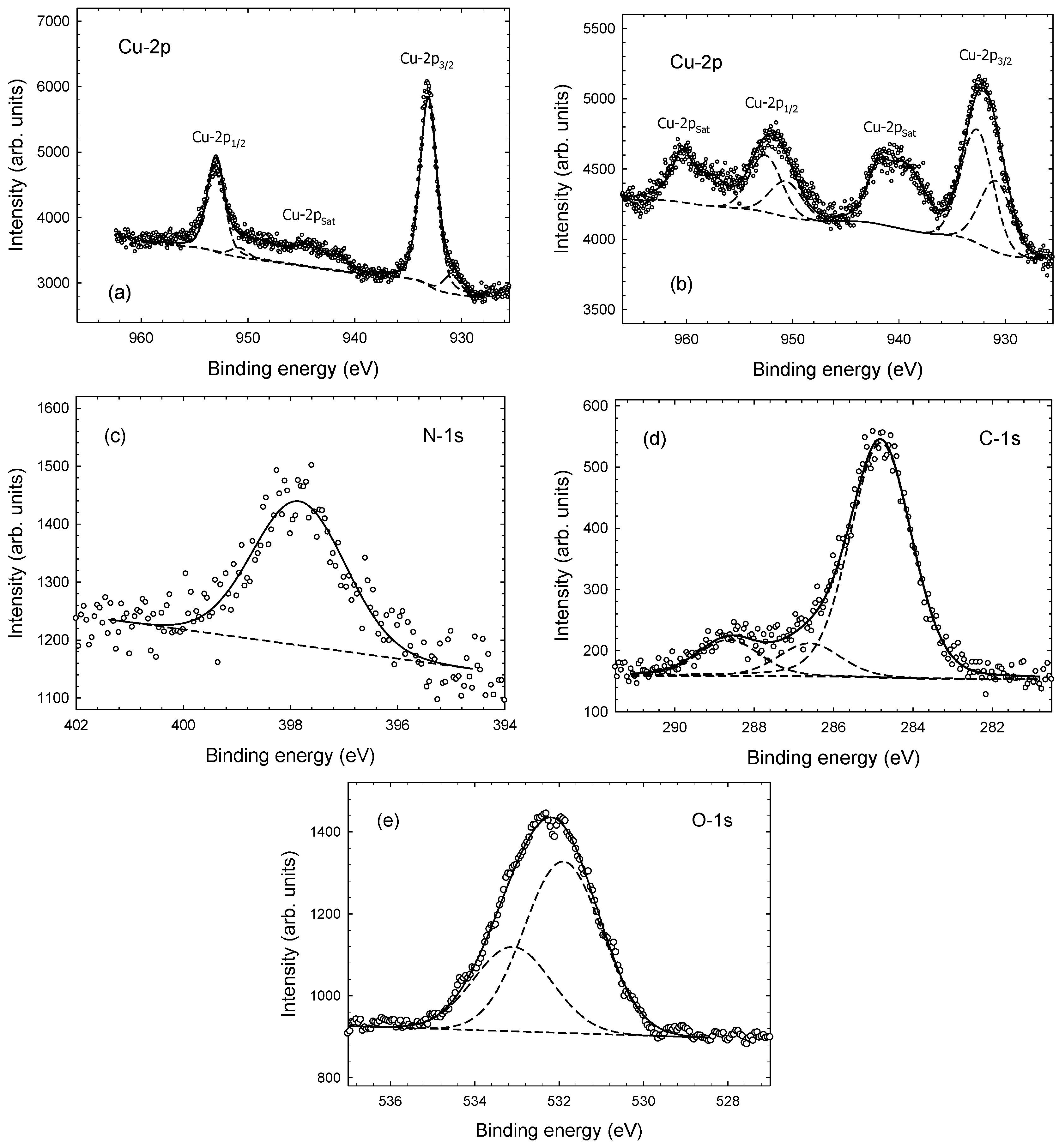
3. Results and Discussion

Photographs of the deposited Cu3N/Si film after exposure to ambient air are displayed in Figure 1. Photographs were taken at intervals of about 10–15 min. Gradual changes of the surface morphology with time are noted. Similar changes are observed for films deposited on glass substrates (not shown here). Figure 1a was taken right after the film was exposed to ambient air at room temperature (≈295 K). Self-buckling of the deposited films was observed after about 12 min (Figure 1b). The buckled area increased gradually with time (Figure 1b–e). Almost the entire film surface was buckled after 90 min, as is obvious from Figure 1f. The buckled area as a function of time is displayed in Figure 2.
Figure 3 shows the SEM picture of the buckled Cu3N surface area. Random ripple structures are observed at tilt angles of 0.6° and 30°. This shows that the film surface is partially taking off towards upwards directions from the substrate, and empty spaces or voids in between the film and the underlying substrate are created. The observed ripple structure is caused by this empty space. Nevertheless, the film still firmly adheres to the substrate. Apparently, the film properties change when exposed to air at atmospheric pressure, which leads to buckling and a partial peeling off the substrate.
Figure 4 shows the X-ray diffraction pattern of the polycrystalline Cu3N film deposited on Si and glass substrates. XRD measurements were carried out shortly after deposition in the case of the Cu3N/Si film and after 5 years in ambient air in the case of the Cu3N/glass film. No significant differences between the two films were observed (see Table 1), demonstrating the good stability of the deposited Cu3N films. The dashed line shows the simulated X-ray patterns of the Cu3N/Si film, which were calculated on the basis of single crystal structure data [18,19]. A lattice parameter a0 = 0.3819 nm was used as a reference value for a stoichiometric and stress-free sample. Free parameters of the simulation (fit) are background, lattice parameter, profile function, and line profile width. Copper nitride has a cubic anti-ReO3 type structure (SG: Pm-3m, No. 221) which is reproduced in the insert of Figure 4. No other crystalline phases were detected. In the ideal crystal structure, the Cu atoms completely occupy the 3c Wyckoff-position with 0 ½ ½; ½ 0 ½; ½ ½ 0. The N atom is in 1b position, with ½ ½ ½. This implies that the (100) and (200) lattice planes differ concerning their occupation with Cu and N atoms. The intensity ratios correspond to bulk values with a statistical distribution of crystallites (Table 1). The X-ray pattern (Figure 4) does not show any preferred orientation. The lattice parameter of the deposited Cu3N films was measured as a0 = 0.3837 nm (Table 1)—significantly larger than that measured by Zachwieja et al. [19] and Navio et al. [20]. Moreno-Armenta et al. [21] reported non-stoichiometric copper nitride (Cu3N) with a lattice parameter a0 = 0.384 nm, which is in reasonable agreement with the present results. Pierson proved the existence of non-stoichiometric copper nitride with lattice constants ranging from as low as 0.375–0.384 nm which are attributed to sub-stoichiometric and over-stoichiometric Cu3N, respectively [22]. Stoichiometric Cu3N means that all regular lattice positions are completely occupied—i.e., the site occupation factor (SOF) is 1 for both lattice positions. Over-stoichiometry means that additional nitrogen atoms are inserted into the Cu3N lattice, probably as interstitials. Both findings indicate that defects play an important role in the development of increasing lattice parameters during the film deposition process, and may lead to the formation of intrinsic stress.
The problem of the cubic Cu3N films is the poor adhesion strength to the substrate, which causes buckling and a partial peeling off the layers. Mechanical properties strongly depend on the micro-structure, which can be extracted from the XRD pattern. The behaviour can result from intrinsic stress and micro-strain in the films. Thin films are almost invariably in a state of stress. The present investigation therefore focuses on intrinsic stress and strain properties of the deposited film (uniform and non-uniform strain). X-ray data are influenced by lattice defects. Imperfections of the first type, such as point defects, displacement disorders or substitution disorders, shift the position of the diffraction line. The imperfections may result in intrinsic stress and strain, which also influences the diffraction line shape (width). Domain sizes and dislocations also influence the diffraction line shape. Notably, all the peaks shift to smaller angles in the deposited film in comparison to stress-free material [19]. Local changes of the atomic ordering of the cubic Cu3N lattice during deposition and crystallization result in a change of its molar volume. In this context, the term “molar volume” is meant to indicate the volume occupied by 1 mol of Cu3N plus associated defects. Point defects, displacement disorder, and substitution disorders, but also anisotropic grain growth affect the molar volume of the material. Changes of this imperfection concentration should be accompanied by a change in uniform film stress. In the case of tensile stress, the atoms are farther apart compared to the annealed (stress-free) case, while it is the opposite in the case of compressive stress [23]. It is evident that a molar volume increase of the films bonded to a rigid substrate will result in an overall increase in film stress. The intrinsic stress can be estimated from Bragg-angle shifts. Assuming an isotropic defect concentration, the intrinsic stress Δσ due to an increase ΔV/V of the molar volume (excess volume) can be estimated as [24]:
Δ σ = 1 3 E ( 1 ν ) Δ V V
where E is Young’s modulus and ν is Poisson’s ratio of the film. Unfortunately, we could not find experimental data of E and ν for Cu3N. An estimate based on the measured ΔV/V using theoretical data for E = 156 GPa and ν = 0.28 [25] yields a large intrinsic stress Δσ = 0.96 GPa of our Cu3N films. Tensile stress will relieve itself by micro-cracking of the film [23]. On the other hand, in the case of compressive stress, the atoms are closer to each other compared to the relaxed (stress-free) case. Compressive stress is relieved by buckling [23]. Hence, the present results could imply that the observed lattice expansion is the result of over-stoichiometry [22]. The observed buckling is then caused by compressive stress in the film, which is relieved by surface oxidation after its exposure to ambient air.
The increase of lattice parameters obtained from smooth and rough film parts is not explainable by the stress and elastic anisotropy alone, since it persists after the film’s partial delamination from the substrate. Besides the uniform strain, we also observed a non-uniform strain. A comparison of the integral width β of the Cu3N sample and a reference standard material (LaB6) that contains no defects, strain, or particle size broadening (NIST, Gaithersburg, MD, USA, SRM 660b) measured under the same conditions shows an appreciable broadening effect in the Cu3N profiles (Figure 5a). Here we define the dimensionless integral width β as the ratio of the integral intensity of a line profile and the peak intensity at the peak’s maximum. The corrected integral width βcor = βCu3N − βLaB6 is obtained by subtracting the width of the reference material (LaB6) from the measured Cu3N width.
The Williamson–Hall (WH) analysis [26] immediately gives qualitative information about the size and shape of the crystallites and the presence of non-uniform lattice strain (Figure 5b). The WH-plot has the following main features: (i) there is a wide scatter of points and (ii) a line connecting the data points (dashed line) displays a positive slope. The scattered data points indicate that the crystallites are anisotropic in shape. The positive slope is an indication of domains with many crystallographic defects which, for example, may arise from deviations in stoichiometry. Making use of [26],
β c o r r cos β = λ T + 4 ε sin β
we can estimate the volume-weighted micro-strain ε = |dd0|/d0, where λ = 0.1542 nm is the X-ray wavelength, T ≈ 50 nm (see below) is the assumed mean particle size, and d0 is the interplanar spacing derived from the peak position. The extracted micro-strain is reasonably large (about 1%–2%) and strongly depends on the lattice orientation (Figure 5b).
Anisotropic line broadening of (100) and (200) line profiles may be caused by non-stoichiometry of the Cu3N films (see above). Therefore, it is necessary to investigate both these profiles in more detail. The microstructure and lattice defects are directly extracted from diffraction pattern in terms of a Fourier transform of the scattered intensity without using any peak shape function [27]. Based on the Warren–Averbach (WA) theory [28,29], Klimanek developed a single line profile method [30]. We use this method because the diffraction vector is different for the (100) and (200) reflection in GIXRD.
The Fourier coefficients F(L) of the physical line profile contain information on particle size T and mean strain S, which are constant within a crystallite or sub-grain, and dislocation density D:
F(L) = FT(L) × FS(L) × FD(L)
where L (in units of nm) is defined as
L = n λ 2 ( sin θ 2 sin θ 1 )
and where θ1 and θ2 define the angular range for the experimentally observable line profile, λ is the X-ray wavelength of Cu Kα radiation, and where the integers n are the harmonics of the Fourier coefficients. The logarithm of F(L) can be expressed as [30]
ln F ( L ) n L = 1 T + K e 2 ( L )
where K is a constant which depends on the interplanar spacing. The linear part of a graph of lnF(L)/nL allows for a determination of the mean particle size T from the intercept and the area-weighted mean squared micro-strain e2(L) due to internal stress from the slope. The dislocation density can be estimated from the linear branch of a Krivoglaz–Wilkens plot [31,32],
ln F ( L ) L 2 = 1 T L + ( K e 2 ( L ) + B ln L 0 ) B ln L
where the factor B is proportional to the mean total dislocation density and L0 is a length which is proportional to the core radius r0 of the strain field of a dislocation.
Figure 6 shows the WA-plot of the (100) and (200) reflections. We must keep in mind that both these planes differ concerning their occupation with nitrogen atoms. The extracted effective particle sizes are T ≈ 50 nm, but there is a significant difference in the area-weighted micro-strain. This implies that deviations in stoichiometry are responsible for the observed line broadening. There is no indication that dislocation densities determined from Krivoglaz–Wilkens plot are different in the (100) and (200) reflections. We calculate dislocation densities of 1.6 × 10¹²/cm2. In the order of magnitude, they correspond to plastic deformation of the films.
Non-uniform and uniform strain are large to the extent of deviations from stoichiometry. A possible explanation is related to film inhomogeneity in dependence on stoichiometry and the orientation of the crystallites. Possible reasons for this inhomogeneity are non-randomly-oriented two-dimensional lattice defects. The occurrence of these defects in dependence on the grain orientation with respect to the specimen surface can cause the inhomogeneity of the films. The parts of a film after peeling-off have a plate-like shape.
The recorded X-ray photoelectron spectra of the copper nitride film show photoelectron emission from the Cu-2p, N-1s, O-1s, and C-1s states (Figure 7). Relative surface compositions of the deposited Cu/N films are given in Table 2. The large amount of carbon and oxygen and the relatively small amounts of Cu and N needs some explanation. XPS is a surface analytical technique, and is thus sensitive to surface contaminations—in particular, adventitious carbon. An analysis of the carbon peak (Figure 7d) shows that it is composed of three contributions, which are attributed to C–C, C–O, and C=O bonds [33,34]. Quantitatively, about 30% of the carbon has bonds with oxygen. The O-1s peak can be decomposed into two peaks which can be associated with oxygen bound to either copper or carbon [35,36,37]. The nitrogen peak (Figure 7c) resembles a single peak with a peak width of ≈2 eV.
The relatively small amount of Cu and N detected by XPS is hence explained by surface contamination with carbon and oxygen of the copper nitride films. The argument is further supported by the observed differences between the copper nitride films deposited on Si or glass samples. The larger contamination of the CuxN-on-glass with carbon and oxygen is explained by the much longer exposure to ambient air. Further proof comes from XPS measurements of the CuxN/glass sample being performed at two different detector angles of 90° and 20° with respect to the substrate. Measurements at smaller detection angles are more sensitive to surface contributions. The enhanced carbon contribution of the 20° measurement indicates that much or all of the carbon is sitting on the surface. The extracted Cu/N ratio is in the range of 2.2–2.4, and hence significantly smaller than the expected ratio of 3 for a Cu3N film. Similar ratios of 2.2–2.7 were measured by Navio et al. [20].
Figure 7a displays the Cu-2p spectrum for the as-deposited CuxN film on a Si substrate; it was measured after the sample had been taken out of the deposition chamber and exposed to ambient air. Figure 7b displays the same Cu-2p region for a CuxN film on a glass substrate after five years in ambient air. Both spectra show the Cu-2p1/2 and Cu-2p3/2 peaks. In addition, there are Cu shake-up satellite lines which are attributed to copper oxide Cu(II)O [35]. Some differences are immediately noted. Most significantly, the width of the Cu-2p peak is 2 eV and 4.4 eV (Figure 7a,b, respectively), significantly different for the two samples. In addition, the intensity of the satellite peaks is larger in Figure 7b compared to Figure 7a. The observations are attributed to the larger oxygen content at the film surface of the CuxN/glass sample, presumably due to the much longer time in air. The strong appearance of the satellite lines provides evidence that a significant fraction of the surface copper is oxidised.
While the XRD results (Figure 4) leave little doubt that much of the deposited film is composed of crystalline Cu3N, the XPS results provide clear evidence that the film has become oxidised on its surface during its exposure to ambient air. We believe that this oxidation is the main reason for the observed stress in the films and for the peeling-off. This idea is supported by the observed time dependence of the peeling-off process (Figure 1), which takes several minutes to complete. Deviations from a stoichiometric Cu3N composition seem to play a significant role in the observed lattice parameter expansion. The nature of this departure from stoichiometry is not fully clear, however. In particular, the question remains whether oxygen is chemisorbed only on the film surface in a thin superficial layer, or to which extent the whole lattice is affected.

4. Conclusions

CuxN films have been deposited by DC magnetron sputtering. After exposure to ambient air, the films partially peel-off, but remain firmly attached to the substrate. XRD measurements show that the bulk material is crystalline Cu3N. However, the X-ray pattern shows remarkable deviations from the ideal poly-crystalline structure. Information about uniform and non-uniform strain is obtained from line shifts and line broadening. Films are characterized by a large intrinsic stress of about 1 GPa and an anisotropic micro-strain of about 1%–2%, presumably caused by stoichiometric deviations in the films. XPS measurements reveal a considerable surface oxidation and the presence of Cu(II)O phases. We suspect that surface oxidation is responsible for the observed stress and micro-strain in the film. Possible reasons for the observed non-uniform and uniform strain are deviations from perfect stoichiometry introduced by surface oxidation. More experiments will be required to prove a causal relationship, however.

Acknowledgments

The work was partly supported by the Deutsche Forschungsgemeinschaft (DFG) through Sonderforschungsbereich SFB/TRR24.

Author Contributions

Abhijit Majumdar and Rainer Hippler conceived and designed the experiments; Abhijit Majumdar performed the experiments; Abhijit Majumdar, Steffen Drache, Harm Wulff, Arun Kumar Mukhopadhyay, Satyaranjan Bhattacharyya, Christiane A. Helm and Rainer Hippler analyzed the data; Abhijit Majumdar, Harm Wulff and Rainer Hippler wrote the paper.

Conflicts of Interest

The authors declare no conflict of interest.

References

  1. Maruyama, T.; Morishita, T. Copper nitride and tin nitride thin films for write-once optical recording media. Appl. Phys. Lett. 1996, 69, 890–891. [Google Scholar] [CrossRef]
  2. Ma, X.D.; Bazhanov, D.I.; Fruchart, O.; Yildiz, F.; Tokoyama, T.; Przybyiski, M.; Stepanyuk, V.S.; Hergert, W.; Kirschner, M. Strain relief guided growth of atomic nanowires in a Cu3N-Cu(110) molecular network. Phys. Rev. Lett. 2009, 102, 205503. [Google Scholar] [CrossRef] [PubMed]
  3. Borsa, D.M.; Grachev, S.; Presura, C.O.; Boerma, D.O. Growth and properties of Cu3N films and Cu3N/γ′-Fe4N bilayers. Appl. Phys. Lett. 2002, 80, 1823–1825. [Google Scholar] [CrossRef]
  4. Maya, L. Covalent nitrides for maskless laser writing of microscopic metal lines. MRS Proc. 1992, 282, 203–208. [Google Scholar] [CrossRef]
  5. Maruyama, T.; Morishita, T. Copper nitride thin films prepared by radio-frequency reactive sputtering. J. Appl. Phys. 1995, 78, 4104–4107. [Google Scholar] [CrossRef]
  6. Kamat, H.; Wang, X.; Parry, J.; Qin, Y.; Zeng, H. Synthesis and characterization of copper-iron-nitride thin films. MRS Adv. 2016, 1, 203–208. [Google Scholar] [CrossRef]
  7. Ji, X.; Ju, H.; Zou, T.; Luo, J.; Hong, K.; Yang, H.; Wang, H. Effects of sputtering pressure on Cu3N thin films by reactive radio frequency magnetron sputtering. Adv. Mater. Res. 2015, 1105, 74–77. [Google Scholar] [CrossRef]
  8. Leng, J.; Chen, L.; Zhu, X.; Sun, Z. Structure and photoelectric properties of Cu3N thin films by reactive magnetron sputtering. Mater. Sci. Forum 2015, 814, 620–624. [Google Scholar] [CrossRef]
  9. Chen, L.; Leng, J.; Yang, Z.; Meng, Z.; Sun, B. Influence of sputtering power on the structure, optical and electric properties of Cu3N films. Mater. Sci. Forum 2015, 814, 596–600. [Google Scholar] [CrossRef]
  10. Soukup, L.; Sicha, M.; Fendrych, F.; Jastrabik, L.; Hubicka, Z.; Studnicka, V.; Wagner, T.; Novak, M. Copper nitride thin films prepared by the RF plasma chemical reactor with low pressure supersonic single and multi-plasma jet system. Surf. Coat. Technol. 1999, 116, 321–326. [Google Scholar] [CrossRef]
  11. Gallardo-Vega, C.; de la Cruz, W. Study of the structure and electrical properties of the copper nitride thin films deposited by pulsed laser deposition. Appl. Surf. Sci. 2006, 252, 8001–8004. [Google Scholar] [CrossRef]
  12. Sahoo, G.; Meher, S.R.; Jain, M.K. Room temperature growth of high crystalline quality Cu3N thin films by modified activated reactive evaporation. Mater. Sci. Eng. B 2015, 191, 7–14. [Google Scholar] [CrossRef]
  13. Wrehde, S.; Quaas, M.; Bogdanowicz, R.; Steffen, H.; Wulff, H.; Hippler, R. Reactive deposition of TiNx layers in a DC-magnetron discharge. Surf. Interface Anal. 2008, 40, 790–793. [Google Scholar] [CrossRef]
  14. Hippler, R.; Steffen, H.; Quaas, M.; Röwf, T.; Tun, T.M.; Wulff, H. Plasma-Assisted Deposition and Crystal Growth of Thin Indium-Tin-Oxide (ITO) Films. In Advances in Solid State Physics 44; Kramer, B., Ed.; Springer: Heidelberg, Germany, 2004; p. 299. [Google Scholar]
  15. Bräuer, G.; Szyszka, B.; Vergöhl, M.; Bandorf, R. Magnetron sputtering—Milestones of 30 years. Vacuum 2010, 84, 1354–1359. [Google Scholar] [CrossRef]
  16. Pflug, A.; Siemers, M.; Melzig, T.; Schäfer, L.; Bräuer, G. Simulation of linear magnetron discharges in 2D and 3D. Surf. Coat. Technol. 2014, 260, 411–416. [Google Scholar] [CrossRef]
  17. Wulff, H.; Steffen, H. Characterization of Thin Films. In Low Temperature Plasmas; Hippler, R., Kersten, H., Schmidt, M., Schoenbach, K.-H., Eds.; Wiley-VCH: Berlin, Germany, 2008; pp. 329–362. [Google Scholar]
  18. Inorganic Crystal Structure Database (ICSD); Version 1.9.8; FIZ: Karlsruhe, Germany, 2016.
  19. Zachwieja, U.; Jacobs, H. Ammonothermalsynthese von Kupfernitrid, Cu3N. J. Less Common Met. 1990, 161, 175–184. [Google Scholar] [CrossRef]
  20. Navío, C.; Capitán, M.J.; Álvarez, J.; Yndurain, F.; Miranda, R. Intrinsic surface band bending in Cu3N(100) ultrathin films. Phys. Rev. B 2007, 76, 085105. [Google Scholar] [CrossRef]
  21. Moreno-Armenta, M.G.; Soto, G.; Takenchi, N. Ab initio calculations of non-stoichiometric copper nitride, pure and with palladium. J. Alloys Comp. 2011, 509, 1471–1476. [Google Scholar] [CrossRef]
  22. Pierson, J.F. Structure and properties of copper nitride films formed by reactive magnetron sputtering. Vacuum 2002, 66, 59–64. [Google Scholar] [CrossRef]
  23. Janssen, G.C.A.M. Stress and strain in polycrystalline thin films. Thin Solid Films 2007, 515, 6654–6664. [Google Scholar] [CrossRef]
  24. Weihnacht, V.; Brückner, W. Abnormal grain growth in {111} textured Cu thin films. Thin Solid Films 2002, 418, 136–144. [Google Scholar] [CrossRef]
  25. Rahmati, A.; Ghoohestani, M.; Badehian, H.; Baizaee, M. Ab initio study of the structural, elastic, electronic and optical properties of Cu3N. Mater. Res. 2014, 17, 303–310. [Google Scholar] [CrossRef]
  26. Williamson, G.K.; Hall, W.H. X-ray line broadening from filed aluminium and wolfram. Acta Metall. 1953, 1, 22–31. [Google Scholar] [CrossRef]
  27. Stokes, R. A Numerical Fourier-analysis method for the correction of widths and shapes of lines on X-ray powder photographs. Proc. Phys. Soc. 1948, 61, 382–391. [Google Scholar] [CrossRef]
  28. Warren, B.E.; Averbach, B.L. The effect of cold-work distortion on X-ray patterns. J. Appl. Phys. 1950, 21, 595–599. [Google Scholar] [CrossRef]
  29. Warren, B.E. X-ray Diffraction; Addison-Wesley: Boston, MA, USA, 1969. [Google Scholar]
  30. Klimanek, P. X-ray diffraction analysis of substructures in plastically deformed BCC materials. J. Phys. IV 1993, 3, 2149–2154. [Google Scholar] [CrossRef]
  31. Krivoglaz, M.A. X-ray and Neutron Diffraction in Nonideal Crystals; Springer: Berlin, Germany, 1966. [Google Scholar]
  32. Wilkens, M. The determination of density and distribution of dislocations in deformed single crystals from broadened X-ray diffraction profiles. Phys. Stat. Sol. a 1970, 2, 359–370. [Google Scholar] [CrossRef]
  33. Thejaswini, H.C.; Bogdanowicz, R.; Danilov, V.; Schäfer, J.; Meichsner, J.; Hippler, R. Deposition and characterization of organic polymer thin films using a dielectric barrier discharge with different C2Hm/N2 (m = 2, 4, 6) gas mixtures. Eur. Phys. J. D 2015, 69, 1–6. [Google Scholar]
  34. Majumdar, A.; Das, G.; Basvani, K.R.; Heinicke, J.; Hippler, R. Role of nitrogen in the formation of HC-N films by CH4/N2 barrier discharge plasma: Aliphatic tendency. J. Phys. Chem. B 2009, 113, 15734–15741. [Google Scholar] [CrossRef] [PubMed]
  35. Biesinger, M.C.; Lau, L.W.M.; Gerson, A.R.; Smart, R.S.C. Resolving surface chemical states in XPS analysis of first row transition metals, oxides and hydroxides: Sc, Ti, V, Cu and Zn. Appl. Surf. Sci. 2010, 257, 887–898. [Google Scholar] [CrossRef]
  36. Wurth, W.; Schneider, C.; Treichler, R.; Umbach, E.; Menzel, D. Evolution of adsorbate core-hole states after bound and continuum primary excitation: Relaxation versus decay. Phys. Rev. B 1987, 35, 7741–7744. [Google Scholar] [CrossRef]
  37. Wagner, C.D.; Zatko, D.A.; Raymond, R.H. Use of the Oxygen KLL Auger lines in identification of surface chemical states by electron spectroscopy for chemical analysis. Anal. Chem. 1980, 52, 1445–1451. [Google Scholar] [CrossRef]
Figure 1. Photographs of deposited CuxN film on Si substrates taken (a) 1 min; (b) 12 min; (c) 24 min; (d) 35 min; (e) 45 min; and (f) 60 min after the film was taken out of the deposition chamber and exposed to ambient air.
Coatings 07 00064 g001
Figure 2. Buckled film area (in percent of the total area) versus exposure time.
Coatings 07 00064 g002
Figure 3. SEM images of deposited CuxN film taken at tilt angles of (a) 0.6° and (b) 30°.
Coatings 07 00064 g003
Figure 4. Measured and simulated (solid line) X-ray diffraction pattern of polycrystalline Cu3N films deposited on a Si and on a glass substrate. Simulation results (dashed line) are also shown for the Cu3N/Si data. To ease comparison, the Cu3N/Si data spectra have been shifted upwards by +100.
Coatings 07 00064 g004
Figure 5. (a) Integral width β of Cu3N and reference material LaB6 vs. diffraction angle. LaB6 (SRM 660b) is used for the determination of the instrument profile function; (b) Williamson–Hall analysis and the extracted micro-strain of the Cu3N thin film. Dashed line is added to guide the eye only.
Coatings 07 00064 g005
Figure 6. Warren–Averbach plot of the (100) and (200) reflections.
Coatings 07 00064 g006
Figure 7. X-ray photoelectron spectroscopy (XPS) spectra of deposited CuxN films (detection angle 90°). (a) Cu-2p (Si substrate); (b) Cu-2p (glass substrate); (c) N-1s (Si substrate); (d) C-1s (Si substrate); (e) O-1s (Si substrate).
Coatings 07 00064 g007
Table 1. XRD results of deposited Cu3N films on (a) Si and (b) glass substrates.
SampleHKL2θ (°)D (nm)Relative IntensityFWHM (°)
(a) Cu3N/Si10023.1660.3836(4)63.00.621
11032.9930.2712(8)21.90.938
11140.7020.2215(0)100.01.083
20047.3530.1918(2)60.31.161
21053.3550.1715(7)22.21.200
(b) Cu3N/glass10023.1590.3837(6)61.70.657
11032.9830.2713(6)21.70.928
11140.6900.2215(6)100.01.103
20047.3380.1918(8)61.01.243
21053.3380.1716(2)22.71.364
Table 2. Relative surface composition of deposited CuxN films as derived from XPS analysis.
SampleAngleCu (%)N (%)Cu/NC (%)O (%)
CuxN/Si90°30.413.82.220.435.5
CuxN/glass20°10.24.62.241.044.2
CuxN/glass90°14.05.82.432.647.6

