Article

Deposition and Characterization of Si-Doped Diamond Films Using Tetraethoxysilane onto a WC-Co Substrate

College of Mechanical Engineering, Donghua University, Shanghai 201620, China
*
Author to whom correspondence should be addressed.
Coatings 2016, 6(3), 39; https://doi.org/10.3390/coatings6030039
Submission received: 29 July 2016 / Revised: 26 August 2016 / Accepted: 2 September 2016 / Published: 5 September 2016

Abstract

:
Silicon-doped (Si-doped) diamond films were deposited on a Co-cemented tungsten carbide (WC-Co) substrate using the hot filament chemical vapor deposition (HFCVD) method with a mixture of acetone, tetraethoxysilane (TEOS), and hydrogen as the recant source. The as-deposited doped diamond films were characterized with field emission scanning electron microscopy (FE-SEM), Raman spectrum, and X-ray diffraction (XRD). Furthermore, Rockwell C indentation tests were conducted to evaluate the adhesion of the Si-doped diamond films grown on the WC-Co substrate. The results demonstrated that the silicon concentration in the reactant source played an important role in the surface morphology and adhesion of diamond films. The size of diamond grain varied from 3 μm to 500 nm with silicon concentration increasing from 0 to 1.41 atom %. When the silicon concentration rose to 1.81 atom %, the grain size became bigger than that of the lower concentration. The ratio of diamond peak {220}/{111} varied with different silicon concentrations. Raman study features revealed high purity of as-deposited diamond films. The Raman spectra also demonstrated the presence of silicon in the diamond films with Si–Si, Si–C and Si–O bonds. Si-doped diamond films with strong adhesive strength on the WC-Co substrate was beneficial for diamond films applied on cutting tools and wear resistance components.

1. Introduction

Diamond films were once widely used as protective coatings for cutting tools due to excellent properties such as high hardness, low wear rate, high thermal conductivity, and good chemical stability. Co-cemented tungsten carbide (WC-Co) was considered the ideal substrate material for producing diamond coated tools [1,2,3]. However, poor adhesion of film/substrate was the main obstacle in the useful application of diamond films as wear-resistant coatings for carbide tools. The graphite formation induced by the binder phase Co and mismatch of the thermal expansion coefficients between the film and the substrate lead to weak adhesive strength [4]. In order to improve the adhesion between diamond films and WC-Co substrates, some pretreatment methods have been applied before diamond deposition. The widely used method was firstly introduced by Peters and Cummings [5], by first using treatment with Murakami’s reagent [K3Fe(CN)6:KOH:H2O = 1:1:10) and then by etching with Caro’s acid (H2SO4 + H2O2 solution). Sun et al. proposed a four-step method including acid etching, abrading, decarburizing by microwave plasma, and ultrasonic treating. The results indicated that the adhesive strength of diamond films was greatly reinforced by WC decarburizing and recarburizing processes [6]. Other papers published in the literature have proposed interlayers to improve adhesion on a diamond or substrate interface. Cabral et al. has reported that thin SiC interlayer could be a suitable option for adherent diamond coatings on cemented carbide tools [7]. Tang et al. tested whether the W/Al interlayer was helpful for enhancing diamond nucleation and adhesion on WC-Co tools [8]. Lin et al. investigated the adhesion of diamond films on a cemented WC substrate with different thicknesses of Ti–Si interlayers. They concluded that Ti and Si may form strong TiC and SiC bonding to enhance film adherence [4]. Polini et al. studied the use of CrN/Cr and CrN interlayers in HFCVD diamond films onto a WC-Co substrate. It was concluded that the unpeened single-layer CrN and MC pretreatment for the substrate can improve the adhesion and wear endurance [9]. Tang et al. claimed that the diamond-coated inserts with boride interlayer displayed excellent performance due to the good adhesion and low stresses of the diamond coatings [2].
As to doped diamond films, nitrogen, oxygen, H2S, and boron were used as the dopant by some researchers [10,11,12,13]. For silicon dopant, it was widely used for improving the properties of diamond-like carbon (DLC) films [14,15,16,17]. Musale et al. studied the effect of silicon doped on the growth and structural characteristics of diamond films on a Si{100} substrate via HFCVD and concluded that silicon can affect the film morphology, the quality of produced diamond, and the photoluminescence band [18]. Orlanducci et al. fabricated Si-doped diamond films on silicon plates by adopting a CH4/H2 mixture and silicon nanoparticles carried by fluxes of Ar using the HFCVD method. They found that the properties of the silicon particles affected the optoelectronic properties of silicon–diamond layers, and the silicon centers gave rise to compressive stress depending on the silicon concentration [19].
Few studies on Si-doped diamond deposition onto WC-Co substrates have been reported. This study proposes a novel method to deposit Si-doped diamond films on a WC-Co substrate. The characterization of as-fabricated Si-doped diamond films was investigated with different techniques. Diamond films on the WC-Co substrate with silicon dopant were of notable influence.

2. Materials and Methods

The substrates used in the work were WC (6 wt %)-Co inserts with the size of 12 mm × 12 mm × 3 mm. Precede to deposition, the WC-Co inserts were pretreated by a two-step chemical etching method. Firstly, the WC-Co inserts were dipped in Murakami’s reagent [10 g K3Fe(CN)6 +10 g KOH + 100 mL H2O] in an ultrasonic vessel for 30 min [20]. The second etching step was performed using acid solution [20 mL HCl + 80 mL H2O2] to wash surface Co out. After that, the inserts were abraded with diamond powders to roughen the surfaces. The deposition process was carried out in a homemade bias-enhanced HFCVD apparatus. In the HFCVD apparatus, tantalum wires were used as the hot filaments, arranged parallel above the WC-Co substrate blades. In order to obtain Si-doped diamond films, tetraethoxysilane (TEOS) was used as the silicon source. The growth of Si-doped diamond was achieved from a mixture of TEOS dissolved in acetone. The silicon concentration [Si/(Si + C)] was calculated according to the amount of TEOS fraction. The amount of TEOS (CTEOS) in the carbide source was defined as the volume of TEOS dissolved in 100 mL of acetone. The increase of CTEOS was from 1 to 20, corresponding to the silicon concentration from 0.11 to 1.81 atom %. The doped diamond-coated inserts were labeled as Sample A to F according to the different silicon concentrations. During the deposition process, a bias current of 4 A was adopted to enhance the diamond nucleation. The detailed deposition parameters of all samples are shown in Table 1.
Field emission scanning electron microscopy (FE-SEM) was adopted to investigate the surface morphology of as-deposited diamond films with various silicon concentrations. The ingredients and purity of the diamond films were examined via Raman spectroscopy and X-ray diffraction (XRD). The adhesive strength was accessed by Rockwell C indentation tests with a load of 1000 N.

3. Results

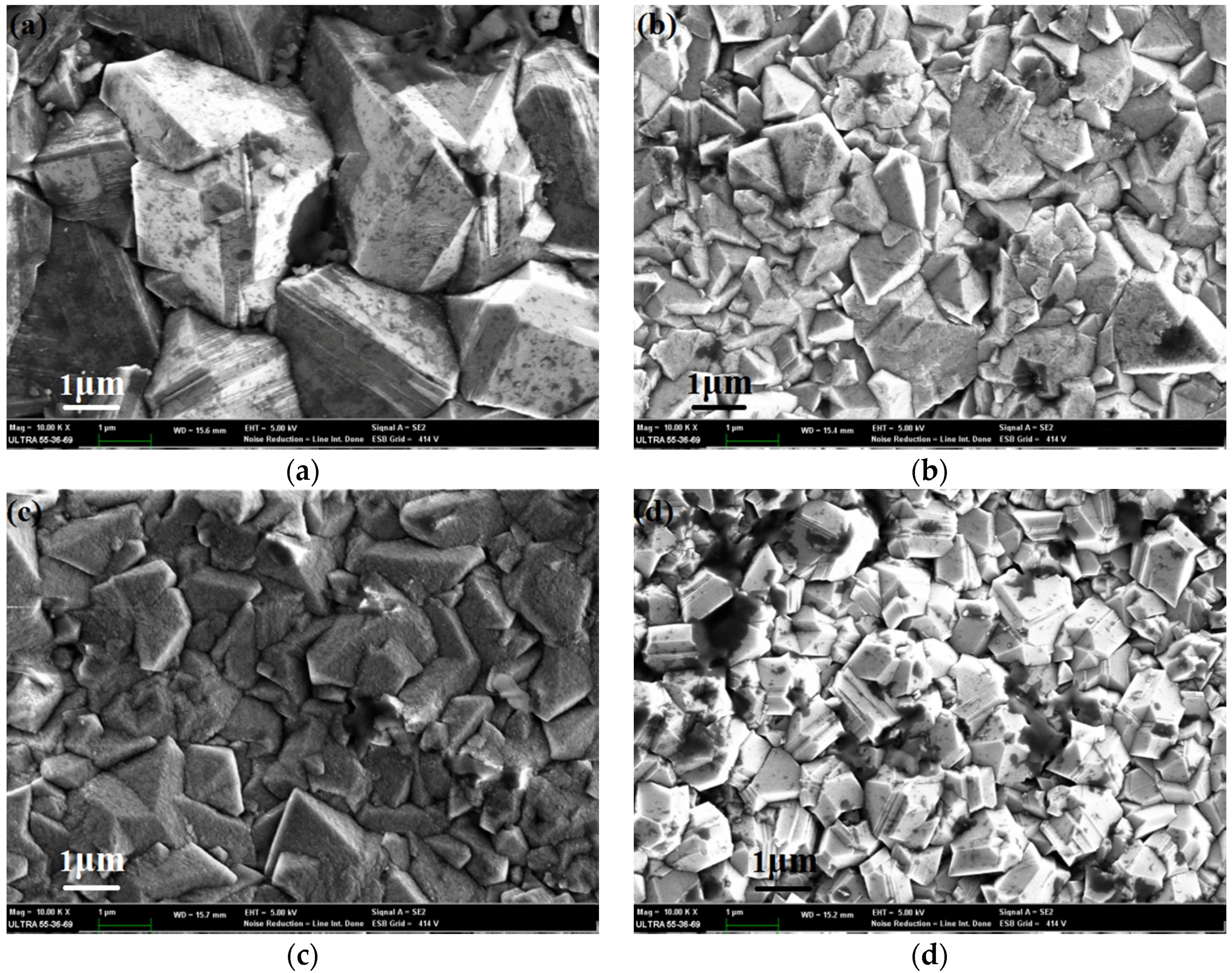
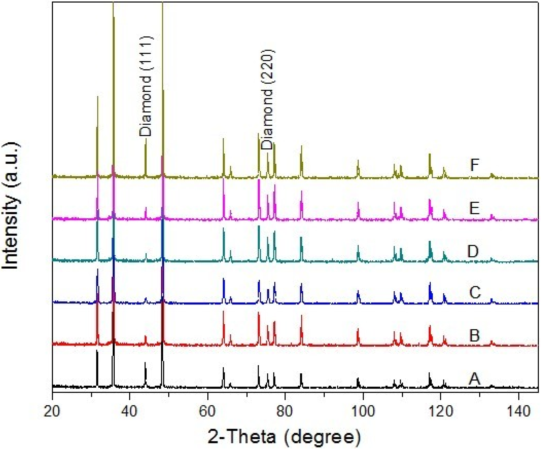
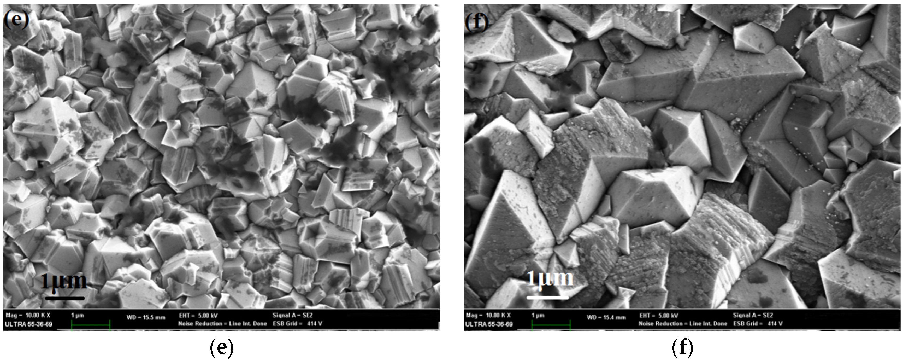
3.1. Surface Characterization
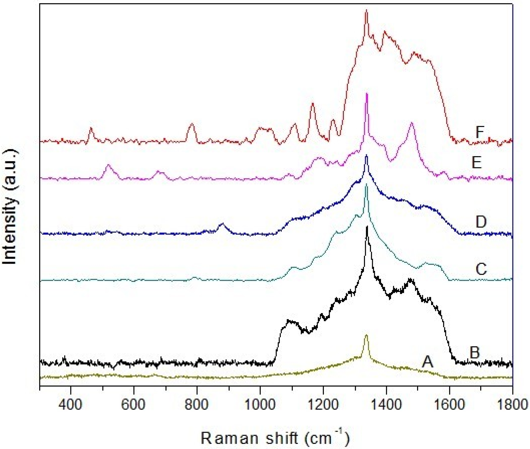
In order to study the effect of silicon on the diamond film morphology, the conventional diamond films were also investigated as comparison. SEM photographs of films grown with different silicon concentrations are shown in Figure 1. Figure 1a is the SEM photograph of a nominal diamond film without the introduction of silicon. It presented pyramid-like large crystallites with {111} facets dominating. The average size of a conventional diamond particle was about 3 μm. For Samples B and C (Figure 1b,c), some small crystalline can be seen on the surface of large crystallites. This is due to the secondary nucleation, affected by the increase in silicon concentration. For higher silicon concentrations, when the CTEOS reached 10 and 15 in accordance with 0.98 to 1.41 atom % silicon, the shape of crystallite changed distinctly as Figure 1d,e shows. The grain size became much smaller, with a size of about 500 nm. The many pits appearing on the top of the small pyramid-like grain were noted. However, when the silicon concentration rose to 1.81 atom %, the grain size became bigger than that of the lower concentration. The silicon with a higher atom % improved the formation of the Si-related compound, but weakened the second nucleation of diamond particles, leading to a larger diamond grain.
In order to check the five major diffraction peaks of diamonds {111}, {220}, {311}, {400}, and {331}, correspondingly at 43.8°, 75.3°, 91.4°, 119.5°, and 140.5°, all samples were examined with a scanning angle from 20° to 145°. The XRD patterns for the diamond films fabricated at various silicon concentrations are shown in Figure 2. The diffraction peaks of diamonds {111} and {220} with different intensities were observed, which, with further evidence, confirmed the diamond nature of these films. Shifts of these peaks to a higher angular position indicated the presence of compress stress, caused by the mismatch of the thermal coefficients of film and substrate material. The ratio of the diamond peak {220}/{111} for different silicon concentrations were 0.5, 1.83, 2.26, 2.92, 1.86, and 0.59 respectively. It suggested that the peak {111} become weaker with silicon dopant, as compared with the conventional diamond films.

3.2. Raman Spectra

The quality of the deposited diamond coating was examined with a Raman spectrum, using a He–Ne laser with an excitation wavelength of 632.8 nm. In order to validate the presence of silicon, the scanning wavenumber was 300 to 1800 cm−1. The Raman spectra of the diamond films deposited at different silicon concentrations are plotted in Figure 3. The wavenumber around 1100 cm−1 related to the Si–O bond [21] is visible for Samples B to F with the silicon addition. As Si concentration increased, the peaks around 790 cm−1 and 870 cm−1 for SiC appeared on Samples C and D.
For higher silicon concentrations, the Raman band near 520 cm−1 and 480 cm−1 for the Si–Si bond [22] occurred on Samples E and F. Furthermore, Raman peaks of 680 cm−1, 780 cm−1, and 960 cm−1 corresponded to the Si–O vibration and Si–C bonds were detected on Samples E and F [23,24]. As to the quality of diamond films, it could be observed from the figure that all samples presented a sharp Raman band around 1331–1336 cm−1 in the spectra, corresponding to the characteristic peak of the diamond phase. The deviation from the sp3 bond (1332 cm−1) suggested the presence of compressive stress during the deposition process. Raman peaks in the 1400–1600 cm−1 region attributed to sp2-bond carbon suggested the existence of the non-diamond phase in the Si-doped diamond films. The intensity of these peaks varied with the increasing silicon concentration. Additionally, peaks of 1180 cm−1 for Sample E and 1200 cm−1 for Sample F indicated the appearance of amorphous sp3 carbon.

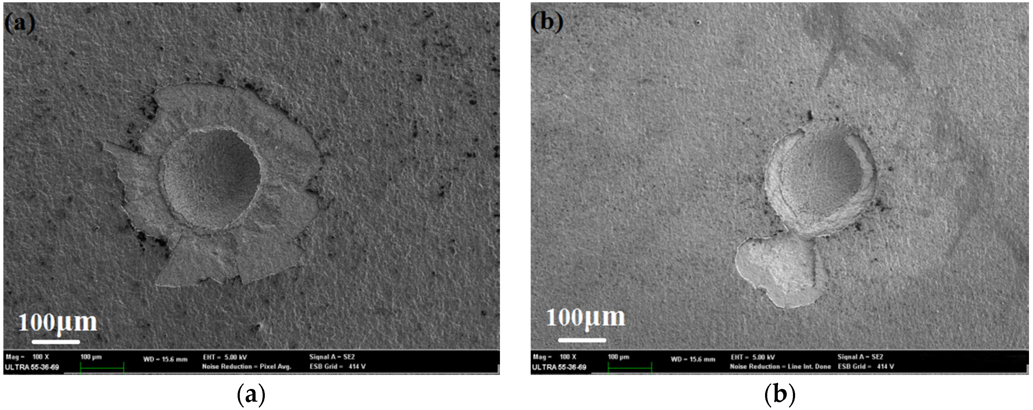
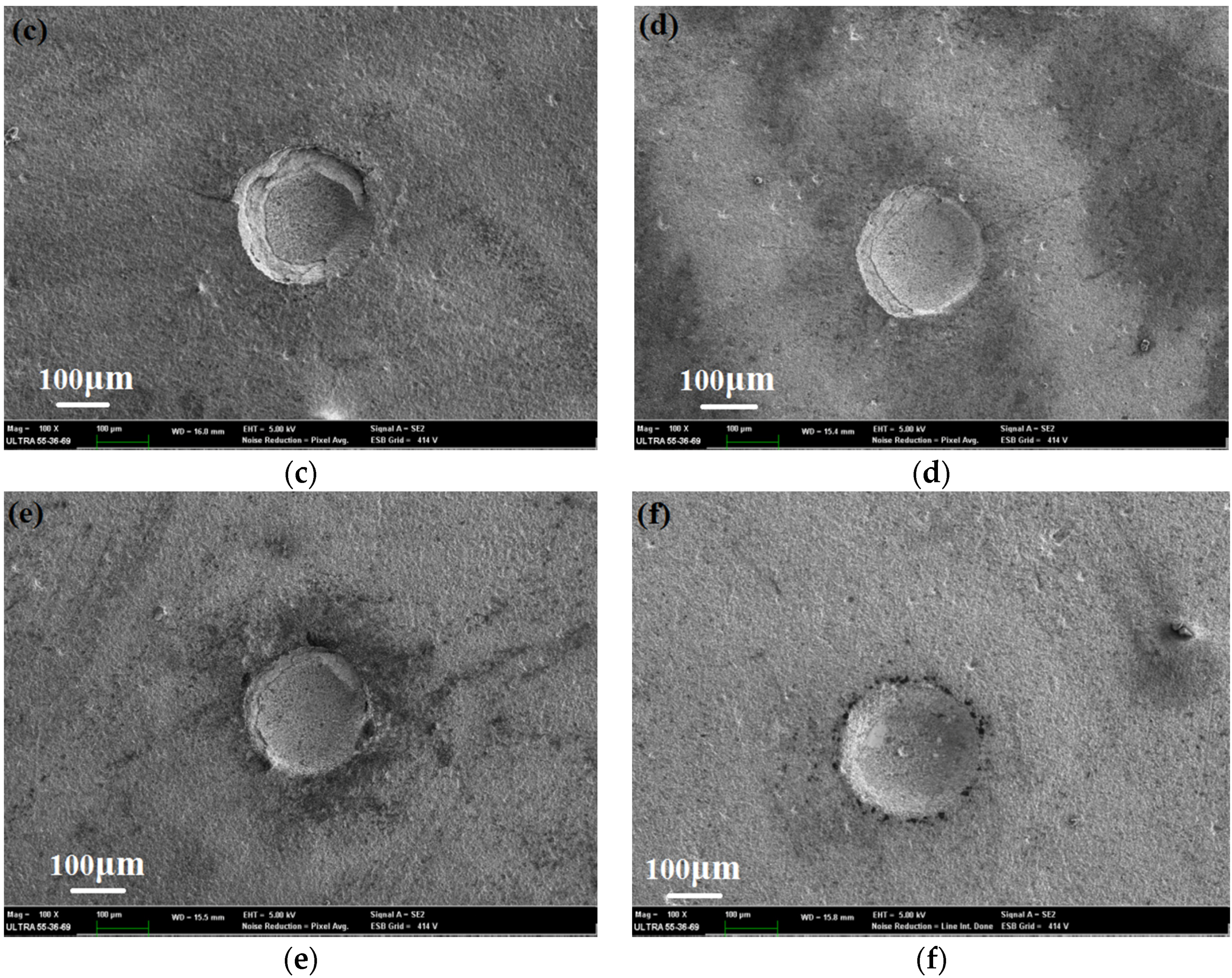
3.3. Adhesive Strength

The adhesive strength of diamond films was evaluated using the Rockwell C indentation method. Figure 4 shows the SEM photographs of indentation tests for the samples at different silicon concentrations under a load of 1000 N. The area of film flaking off can be observed, and the crack became smaller and smaller as silicon concentration increased. In Figure 4a, sever delamination and cracks are clear due to the poor adhesion of the film or substrate. Film flaking-off occurs on Sample B with 0.11% Si adopted, as shown in Figure 4b. For Sample C, with 0.52% silicon concentration, the cracks and peeling were less than that of Sample B. There was neither a crack nor any gap appearance in the vicinity of the indentation contact region when the CTEOS reached 20, as Figure 4f shows. Reduction of the broken area was according to the increment of silicon concentration. The results indicated that the film adhesion to the substrate with a higher silicon concentration have been greatly enhanced.

4. Conclusions

Depositing diamond films with excellent adhesion and a smoother surface on a WC-Co substrate using the HFCVD method can facilitate the useful application of CVD diamond films in the tool field. A novel deposition method for fabricating Si-doped diamond films was proposed in this study, in which TEOS was introduced as a silicon source for depositing doped diamond films. The characterization of Si-doped diamond films varied with the silicon concentration.
With an increase in the atom % of silicon (from 0 to 1.41), surface morphology of diamond films changed from a pyramidal feature with big volume crystallites to a cluster shape with a smaller grain. The silicon dopant affected the non-diamond phase and amorphous sp3 carbon in the diamond films, testified by Raman spectra. Furthermore, the Raman peaks confirmed the existence of silicon, silicon carbide, and silicon oxides in the Si-doped diamond films. This played a role in restricting the over-growth of diamond crystallites. These are the reasons grain refinement films were attained by silicon doping. The 1.81 atom % was the optimized parameter in the concentration range studied according to the highest adhesive strength. The addition of silicon could enhance the diamond nucleation and adhesion on WC-Co substrates and thus facilitate the wide application of diamond-coated WC-Co tools. This technology provided guidance for the growth and application of Si-doped diamonds.

Acknowledgments

The authors acknowledge the financial support from the China Postdoctoral Science Foundation Funded Project (2016M591570), Fundamental Research Funds for the Central Universities (15D210302, 15D110320), Shanghai Key Lab of Advanced Manufacturing Environment (KT20150901), Natural Science Foundation of China (51475301), and Shanghai Leading Academic Discipline Project (B602).

Author Contributions

Jianguo Zhang, Xia Ji, and Xiaohu Zheng conceived, designed, and performed the experiments and wrote the paper; Jinsong Bao analyzed the data.

Conflicts of Interest

The authors declare no conflict of interest. The founding sponsors had no role in the design of the study; in the collection, analyses, or interpretation of data; in the writing of the manuscript, or in the decision to publish the results.

References

  1. Polini, R. Chemically vapour deposited diamond coatings on cemented tungsten carbides: Substrate pretreatments, adhesion and cutting performance. Thin Solid Films 2006, 515, 4–13. [Google Scholar] [CrossRef] [Green Version]
  2. Tang, W.; Wang, Q.; Wang, S.; Lu, F. A comparison in performance of diamond coated cemented carbide cutting tools with and without a boride interlayer. Surf. Coat. Technol. 2002, 153, 298–303. [Google Scholar] [CrossRef]
  3. Polini, R.; Tomellini, M. Analysis of size distribution functions of diamond crystallites formed in the early stages of chemical vapour deposition. Diam. Relat. Mater. 1995, 4, 1311–1316. [Google Scholar] [CrossRef]
  4. Lin, C.R.; Cheng, T.K.; Chang, R.M. Improvement in adhesion of diamond films on cemented WC substrate with Ti–Si interlayers. Diam. Relat. Mater. 1998, 7, 1628–1632. [Google Scholar] [CrossRef]
  5. Peters, M.G.; Cummings, R.H. Methods for coating adherent diamond films on cemented tungsten carbide substrates. European Patent 0519587 A1, 1992. [Google Scholar]
  6. Sun, F.H.; Zhang, Z.M.; Chen, M.; Shen, H.S. Improvement of adhesive strength and surface roughness of diamond films on Co-cemented tungsten carbide tools. Diam. Relat. Mater. 2003, 12, 711–718. [Google Scholar] [CrossRef]
  7. Cabral, G.; Gäbler, J.; Polini, R.; Lindner, J.; Grácio, J. A study of diamond film deposition on WC-Co inserts for graphite machining: Effectiveness of SiC interlayers prepared by HFCVD. Diam. Relat. Mater. 2008, 17, 1008–1014. [Google Scholar] [CrossRef]
  8. Tang, Y.; Li, Y.S.; Yang, Q.; Hirose, A. Deposition and characterization of diamond coatings on WC-Co cutting tools with W/Al interlayer. Diam. Relat. Mater. 2010, 19, 496–499. [Google Scholar] [CrossRef]
  9. Polini, R.; Barletta, M. On the use of CrN/Cr and CrN interlayers in hot filament chemical vapour deposition (HF-CVD) of diamond films onto WC-Co substrates. Diam. Relat. Mater. 2008, 17, 325–335. [Google Scholar] [CrossRef] [Green Version]
  10. Tang, C.J.; Neves, A.J.; Pereira, S.; Fernandes, A.J.S.; Grácio, J.; Carmo, M.C. Effect of nitrogen and oxygen addition on morphology and texture of diamond films (from polycrystalline to nanocrystalline). Diam. Relat. Mater. 2008, 17, 72–78. [Google Scholar] [CrossRef]
  11. Sternschulte, H.; Schreck, M.; Stritzker, B.; Bergmaier, A.; Dollinger, G. Growth and properties of CVD diamond films grown under H2S addition. Diam. Relat. Mater. 2003, 12, 318–323. [Google Scholar] [CrossRef]
  12. Tang, C.J.; Abe, I.; Vieira, L.G.; Soares, M.J.; Grácio, J.; Pinto, J.L. Investigation of nitrogen addition on hydrogen incorporation in CVD diamond films from polycrystalline to nanocrystalline. Diam. Relat. Mater. 2010, 19, 404–408. [Google Scholar] [CrossRef]
  13. Tang, C.J.; Neves, A.J.; Fernandes, A.J.S. Study the effect of O2 addition on hydrogen incorporation in CVD diamond. Diam. Relat. Mater. 2004, 13, 203–208. [Google Scholar] [CrossRef]
  14. Wu, W.J.; Hon, M.H. The effect of residual stress on adhesion of silicon-containing diamond-like carbon coatings. Thin Solid Films 1999, 345, 200–207. [Google Scholar] [CrossRef]
  15. He, X.M.; Walter, K.C.; Nastasi, M.; Lee, S.T.; Fung, M.K. Investigation of Si-doped diamond-like carbon films synthesized by plasma immersion ion processing. J. Vac. Sci. Technol. A 2000, 18, 2143–2148. [Google Scholar] [CrossRef]
  16. Ray, S.C.; Okpalugo, T.I.T.; Papakonstantinou, P.; Bao, C.W.; Tsai, H.M.; Chiou, J.W.; Jan, J.C.; Pong, W.F.; Mclaughlin, J.A.; Wang, W.J. Electronic structure and hardening mechanism of Si-doped/undoped diamond-like carbon films. Thin Solid Films 2005, 482, 242–247. [Google Scholar] [CrossRef]
  17. Zhao, Q.; Liu, Y.; Wang, C.; Wang, S. Bacterial adhesion on silicon-doped diamond-like carbon films. Diam. Relat. Mater. 2007, 16, 1682–1687. [Google Scholar] [CrossRef]
  18. Musale, D.V.; Sainkar, S.R.; Kshirsagar, S.T. Raman, photoluminescence and morphological studies of Si- and N-doped diamond films grown on Si(100) substrate by hot-filament chemical vapor deposition technique. Diam. Relat. Mater. 2002, 11, 75–86. [Google Scholar] [CrossRef]
  19. Orlanducci, S.; Sessa, V.; Tamburri, E.; Terranova, M.L.; Rossi, M.; Botti, S. Si-doped and nanocomposite Si-diamond films: Cathodoluminescence and photoluminescence characterizations of Si centers. Surf. Coat. Technol. 2007, 210, 9389–9394. [Google Scholar] [CrossRef]
  20. Shen, B.; Sun, F. Deposition and friction properties of ultra-smooth composite diamond films on Co-cemented tungsten carbide substrates. Diam. Relat. Mater. 2009, 18, 238–243. [Google Scholar] [CrossRef]
  21. Boizot, B.; Petite, G.; Ghaleb, D.; Reynard, B.; Calas, G. Raman study of β-irradiated glasses. J. Non-Cryst. Solids 1999, 243, 268–272. [Google Scholar] [CrossRef]
  22. Kuzik, L.A.; Yakovlev, V.A.; Mattei, G. Raman scattering enhancement in porous silicon microcavity. Appl. Phys. Lett. 1999, 75, 1830–1832. [Google Scholar] [CrossRef]
  23. Kirkpatrick, R.J.; Yarger, J.L.; Mcmillan, P.F.; Ping, Y.; Cong, X. Raman Spectroscopy of C-S-H, Tobermorite, and Jennite. Adv. Cem. Based Mater. 1997, 5, 93–99. [Google Scholar] [CrossRef]
  24. Feng, Z.C.; Mascarenhas, A.J.; Choyke, W.J.; Powell, J.A. Raman scattering studies of chemical-vapor-deposited cubic SiC films of (100)Si. J. Appl. Phys. 1988, 64, 3176–3186. [Google Scholar] [CrossRef]
Figure 1. SEM surface morphology of Si-doped diamond film with various silicon concentrations: (a) 0 atom %; (b) 0.11 atom %; (c) 0.52 atom %; (d) 0.98 atom %; (e) 1.41 atom %; (f) 1.81 atom %.
Coatings 06 00039 g001aCoatings 06 00039 g001b
Figure 2. XRD patterns of diamond deposited using different silicon concentrations. A: 0 atom %; B: 0.11 atom %; C: 0.52 atom %; D: 0.98 atom %; E: 1.41 atom % and F: 1.81 atom %.
Coatings 06 00039 g002
Figure 3. Raman spectra of diamond deposited using different silicon concentrations. A: 0 atom %; B: 0.11 atom %; C: 0.52 atom %; D: 0.98 atom %; E: 1.41 atom % and F: 1.81 atom %.
Coatings 06 00039 g003
Figure 4. SEM morphology of the Rockwell indentation on Samples A to F with various silicon concentrations: (a) 0 atom %; (b) 0.11 atom %; (c) 0.52 atom %; (d) 0.98 atom %; (e) 1.41 atom %; (f) 1.81 atom %.
Coatings 06 00039 g004aCoatings 06 00039 g004b
Table 1. Detailed deposition parameters.
Sample TitleSi/(Si + C) (atom %)Substrate Temperature (°C)Deposition Time (h)
A0800 ± 506
B0.11800 ± 506
C0.52800 ± 506
D0.98800 ± 506
E1.41800 ± 506
F1.81800 ± 506

