3.1. Morphological and Microstructural Characterization
In
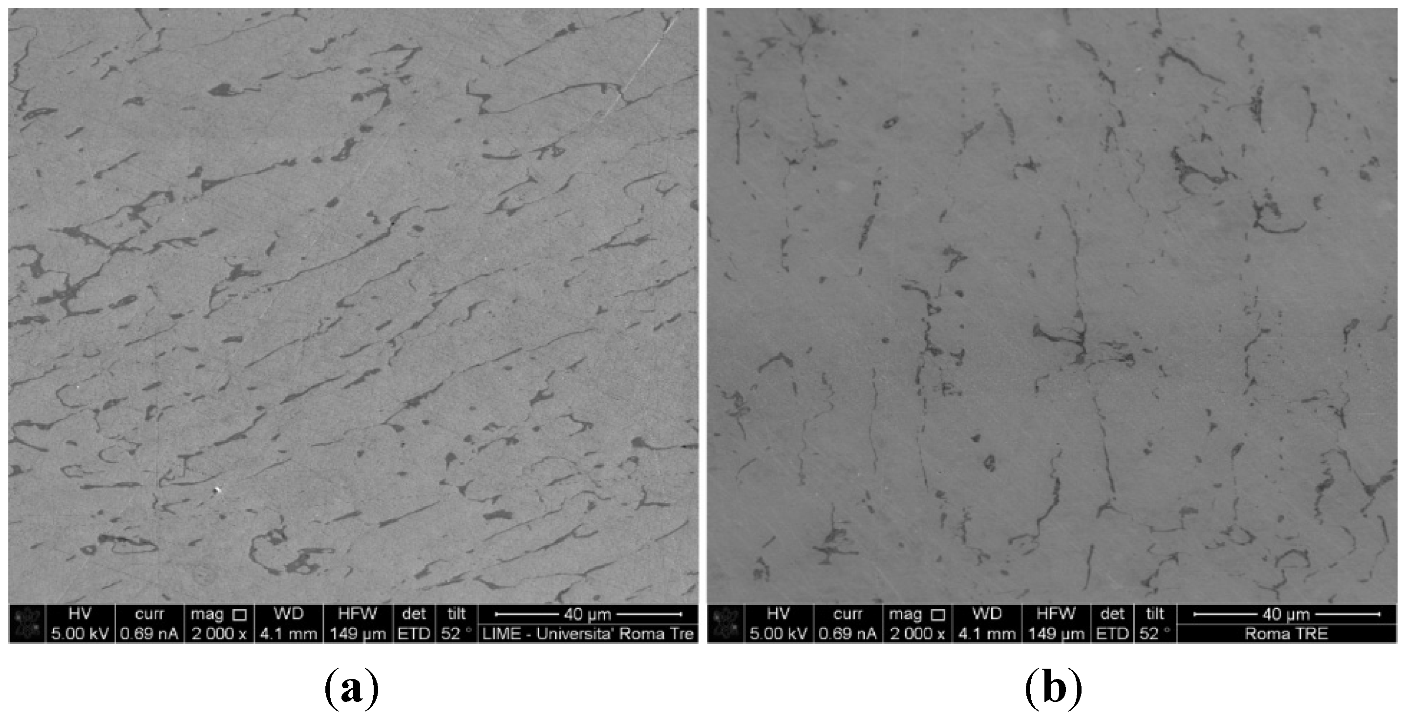
Figure 1, SEM micrographs for the samples 1467 and 1469 are reported, showing that the samples have the typical two-phase structure, with a matrix—were Ag is predominant—and clusters of a second phase, rich in copper. Such morphology suggests that a slow, equilibrium cooling occurred [
21,
22].
Similar microstructures were evidenced for all the samples.
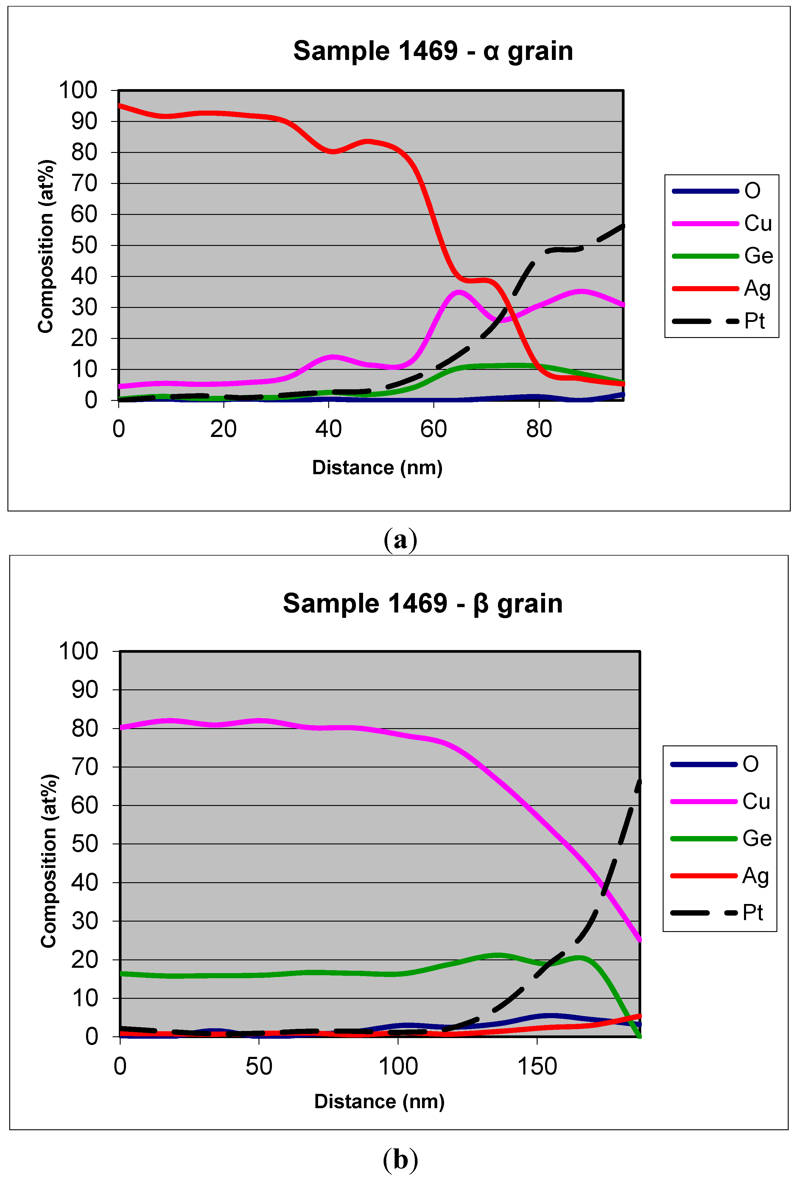
EDS cross-section profiles on TEM lamellae for the 1469 sample are shown in
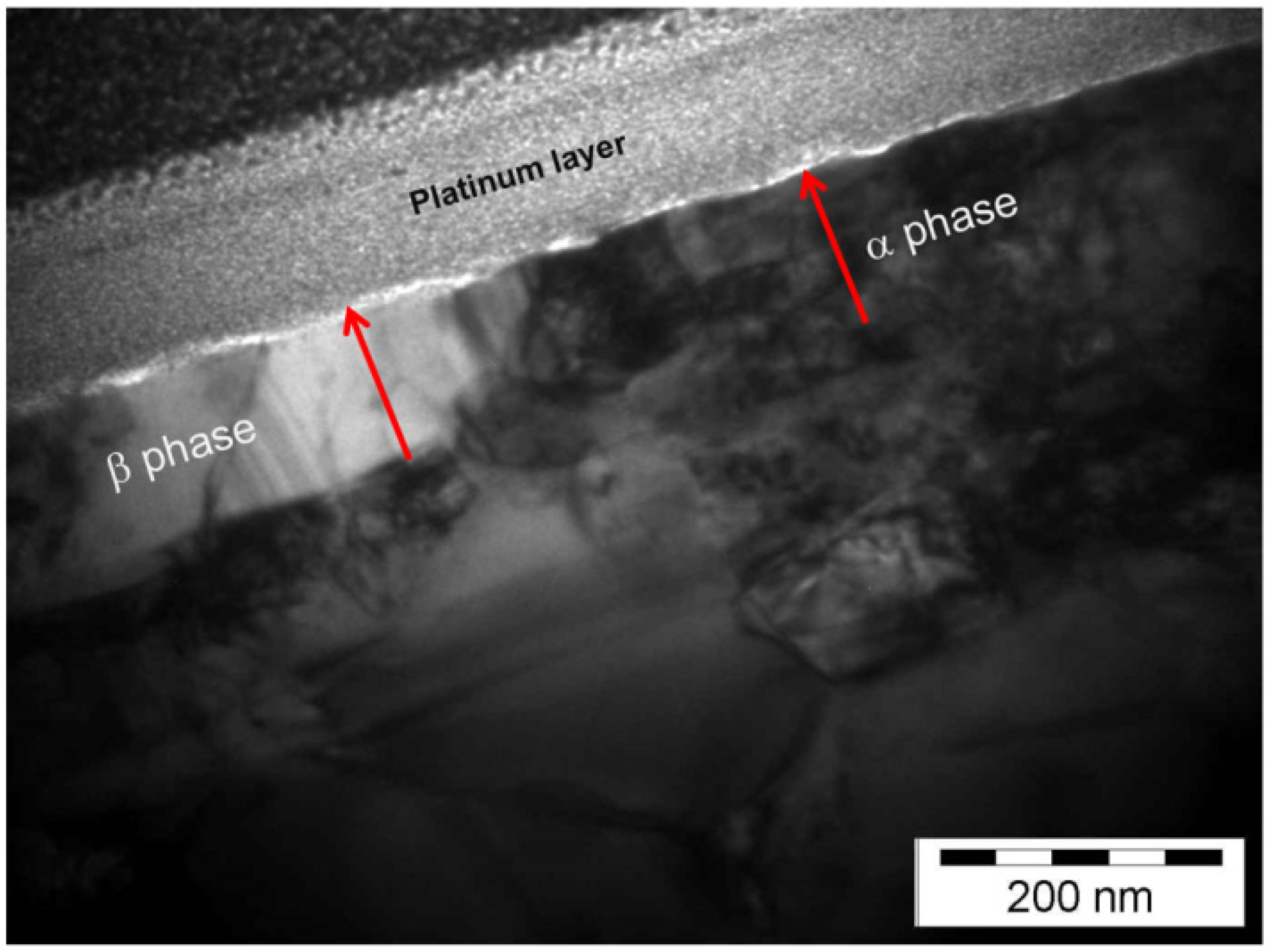
Figure 2. The profiles were performed for both the main phases. At least eight measurement points were performed for each analysis and the points were aligned on a path starting from about 100 nm deep into the surface of the samples and moving towards the platinum protective layers. The red arrows in
Figure 3 show the points (approximately) and the direction of measurements. As shown in
Figure 2 the matrix phase (α-phase) is mainly constituted of Ag, with a small amount of Cu and Ge, while it is in the β-phase, richer in copper, that most of the Germanium is alloyed. It is also in this phase that most of the oxide forms. However, even if some oxide forms in the α-phase, it is still Cu and Ge oxide, since the XPS showed that no Ag is present in its oxidized state. Similar trends were obtained for all the samples, and are not shown here for brevity.
Figure 1.
SEM micrographs of samples (a) 1467 and (b) 1469.
Figure 1.
SEM micrographs of samples (a) 1467 and (b) 1469.
Figure 2.
EDS profile distribution of the elements for (a) α-phase and (b) β-phase of sample 1469.
Figure 2.
EDS profile distribution of the elements for (a) α-phase and (b) β-phase of sample 1469.
Figure 3.
TEM micrograph (120 kV) showing the oxide layer for sample 1469.
Figure 3.
TEM micrograph (120 kV) showing the oxide layer for sample 1469.
Table 1 shows XPS data relative to Ag, Cu, and Ge peaks for all samples. It was found that silver is present only in its metallic state; Cu is present as Cu, CuO, and Cu
2O (it was not possible to separate the peaks of Cu and Cu
2O), while Ge is present in both metallic (Ge) and oxidized (GeO
2) state.
Data reported in
Table 1 show that the heat treatment favors the surface concentration of Cu and Ge; this is probably due to the diffusion of germanium (and to a lesser extent, of copper) from the deeper zones of the bulk towards the surface. This diffusion balanced the amount of Ge and Cu that had reacted with oxygen and was removed from the alloy lattice following the oxidation process. It also seems that the heating treatment favors the oxidation of Ge rather than Cu. In sample 1468, treated at 100 °C, the percentage of oxidized germanium is higher by 5% with respect to the non-heated sample; if the heating is prolonged, as for sample 1469, all the Ge is oxidized. Sample 1470, treated at 200 °C, shows again a little metallic Ge, suggesting that the surface oxide may be fragile and may have cracked, thus exposing part of the underneath metallic phase: this is also confirmed by SEM and AFM images.
Table 1.
XPS data showing the wt. percentage of each element for all the samples.
Table 1.
XPS data showing the wt. percentage of each element for all the samples.
| Sample | wt% Ag | wt% Cu | wt% Ge | wt% Cu(0) + Cu2O | wt% CuO | wt% Ge(0) | wt% GeO2 |
|---|
| 1467 | 78.5 | 19.3 | 2.2 | 68.5 | 31.5 | 34.4 | 65.6 |
| 1468 | 78.1 | 19.2 | 2.7 | 74.3 | 25.7 | 29.3 | 70.7 |
| 1469 | 73.9 | 22.3 | 3.8 | 78.8 | 21.2 | 0 | 100 |
| 1470 | 62.6 | 29.8 | 7.6 | 87.5 | 12.5 | 19.2 | 80.8 |
In
Figure 3a TEM micrograph with the detail of sample 1469 is reported showing the two main phases and the thin oxide layer (the thin white line between the alloy and the protective platinum layer). From such images it was possible, for all samples, to measure the thickness of the oxide layer.
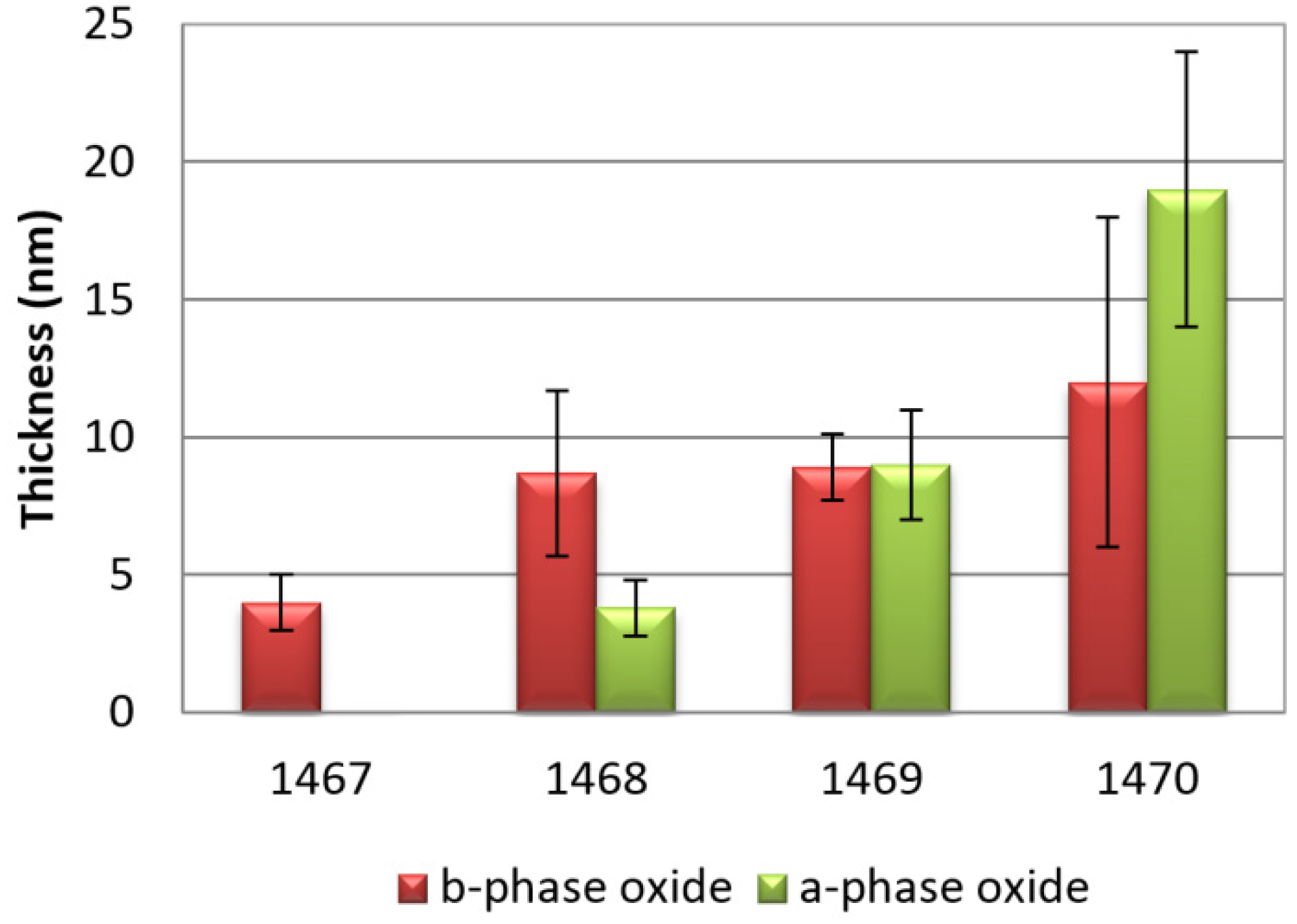
A histogram with the estimated average thickness of the oxide layers is shown in
Figure 4: it is clearly visible that a higher temperature is responsible for the increase of the total oxide layer, rising from 4 ± 1 nm for sample 1467 (no heat treatment) to 19 ± 5 nm for sample 1470 (200 °C).
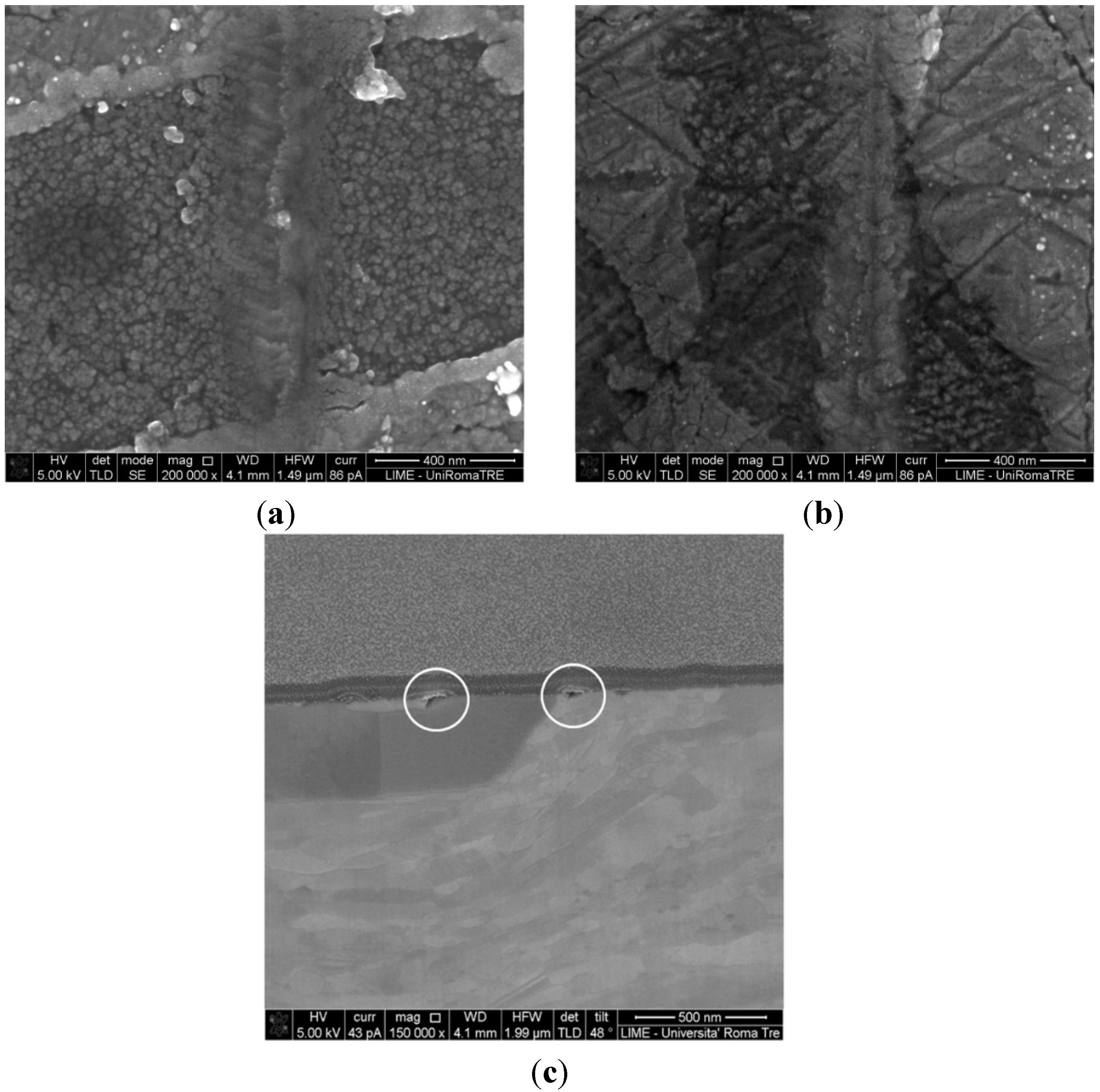
For all samples (1470 excluded) it was shown that the oxide layer is thicker in the β-phase than in the α-phase. Only in sample 1469 is germanium oxide thickness uniformly distributed between the two main phases. For sample 1467, which did not undergo any heating treatment, no protective oxide layer was observed in the main phase. Also, in sample 1470 the oxide is about to crack, revealing it to be porous and fragile, as shown in
Figure 5a; the porous oxide structure is clearly visible. For comparison,
Figure 5b shows an image of sample 1469 whose protective oxide layer is revealed to be thin and dense.
Figure 5c shows a section of sample 1470 in which the cracks in the oxide layer are evidenced in circles.
Figure 4.
Histogram of the oxide thickness for all samples.
Figure 4.
Histogram of the oxide thickness for all samples.
Figure 5.
(a) SEM image of the 1470 oxide layer showing a porous structure; (b) SEM image of the 1469 sample, showing a thin and dense oxide film; (c) Section of sample 1470 showing the film cracks in the points circled.
Figure 5.
(a) SEM image of the 1470 oxide layer showing a porous structure; (b) SEM image of the 1469 sample, showing a thin and dense oxide film; (c) Section of sample 1470 showing the film cracks in the points circled.
A thicker oxide layer, in conjunction with a more porous and more inhomogeneous surface morphology, could lead to a more brittle behavior of the oxide layer itself, as in the case of sample 1470.
AFM images confirm that all samples have the typical two-phase structure, with an Ag-rich matrix (α), and clusters of a β, Cu-rich, phase. In all samples the Cu-rich phase is made of clusters slightly higher than the matrix: this is due to the higher hardness of the β-phase oxide, so that during polishing a minor quantity of material is removed. As we already know from EDS, it is in this second phase that most of the germanium is alloyed.
Figure 6 shows the different morphology, for sample 1468, passivated at 100 °C, for the two different phases. The Cu-rich phase is characterized by roundly shaped grains (about 40–60 nm in diameter) which tend to agglomerate in height to form bigger structures (130–180 nm), while the Ag-rich phase is constituted by grains of 30–50 nm in diameter which tend to agglomerate in a longitudinal direction.
A similar trend is confirmed for all samples, not shown here for brevity. The second phase also show mean roughness values that are slightly higher than those measured for the Ag-rich matrix, as shown in
Table 2. The mean roughness reported here is measured according to the ISO 4287 standard [
23], and it is relative to a 1 × 1 µm area, since the inclusions of the β-phase are very small.
Figure 6.
AFM images (8 µm × 8 µm) of sample 1468. The same image is shown with two different values of color contrast: (a) A brighter contrast was used to evidence the microstructure of α-phase, while (b) a darker contrast is used for β-phase.
Figure 6.
AFM images (8 µm × 8 µm) of sample 1468. The same image is shown with two different values of color contrast: (a) A brighter contrast was used to evidence the microstructure of α-phase, while (b) a darker contrast is used for β-phase.
Table 2 also shows, for all samples, the value of the mean roughness, measured on the maximum area possible to scan with AFM.
Due to a non-planarity of some samples and to the impossibility to perform any surface cleaning prior to the data acquisition with AFM—to avoid altering the result—the maximum scan area that was possible to acquire without any artefacts or contamination in the imaging, was 50 µm × 50 µm. The reported values refer to an average of five different areas for each sample. It is clear, from the data in
Table 2, that an increase of the passivation temperature induces an increase of the mean roughness, rising from 3.7 nm for the sample with no heat treatment to 4.4 nm (average) for the samples passivated at 100 °C, to 7.1 nm for the sample heated at 200 °C. The increase of the mean roughness is in agreement with the presence of a thicker oxide layer in the samples treated at higher temperature, since it was observed that the grains of the β phase tend to agglomerate to form higher, and rougher, structures.
Table 2.
Average roughness parameters calculated on a 50 µm × 50 µm scan area for all the samples.
Table 2.
Average roughness parameters calculated on a 50 µm × 50 µm scan area for all the samples.
| Sample | Heating | Ra [nm] |
|---|
| 1467 | r.t. | 3.7 |
| 1468 | 100 °C | 4.2 |
| 1469 | 100 °C | 4.6 |
| 1470 | 200 °C | 7.1 |
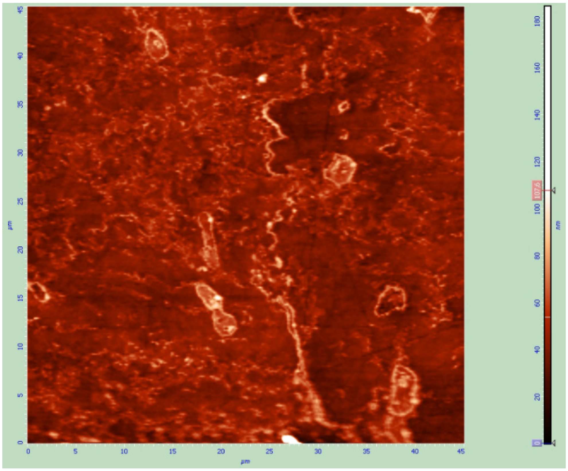
AFM also confirmed that sample 1470 has a fragile surface oxide that tends to exfoliate, as shown in
Figure 7.
Figure 7.
AFM image (45 µm × 45 µm) of sample 1470.
Figure 7.
AFM image (45 µm × 45 µm) of sample 1470.
3.2. Micromechanical Characterization
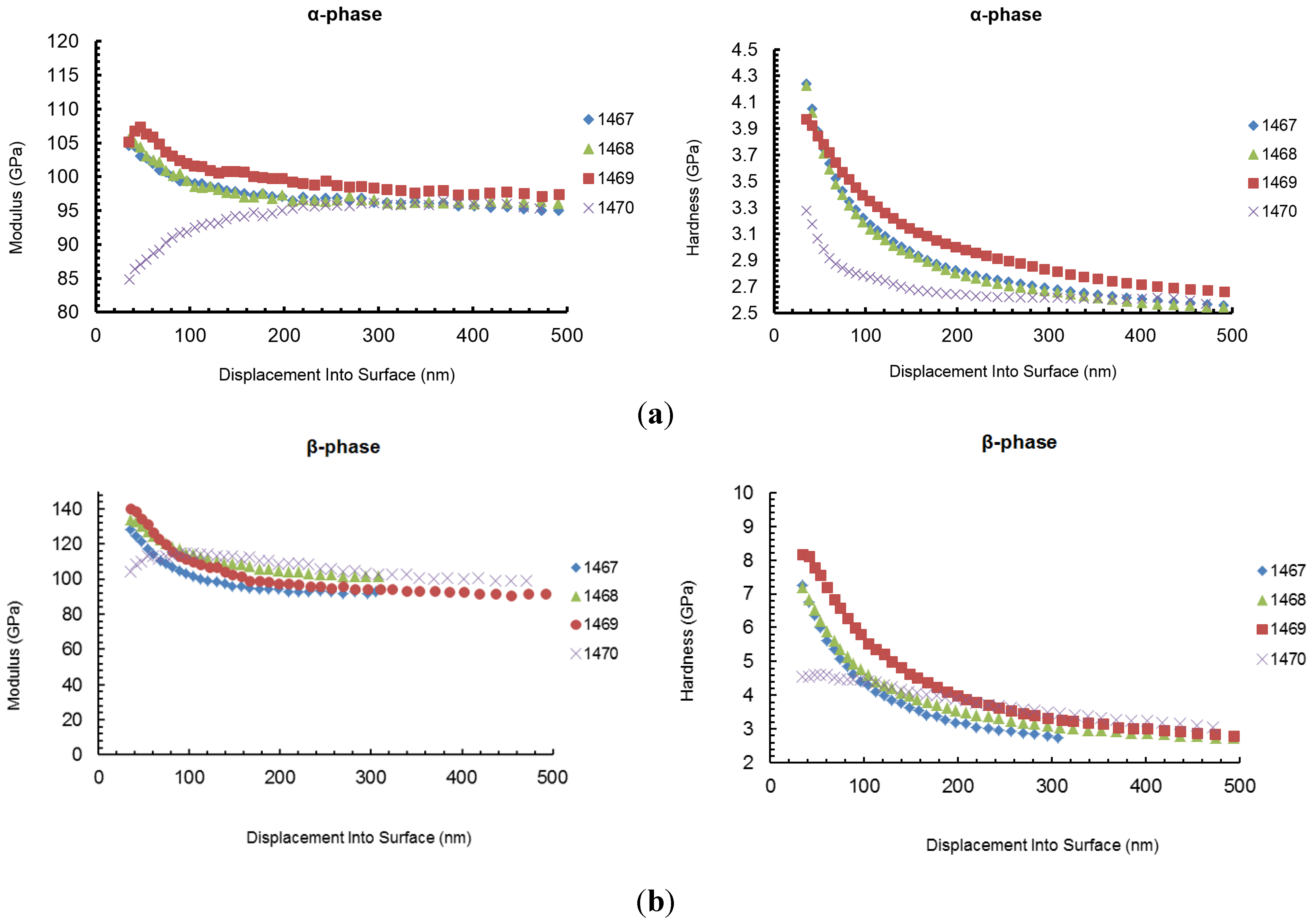
Through nanoindentation hardness and elastic modulus both the main different phases were evaluated for each sample.
Figure 8 shows the comparison between the modulus and hardness of the two main phases for all samples (error bars are not shown for clarity).
The results show that for all samples, the bulk properties are almost the same, as shown in the graphics above, at the higher values of displacement into surface. Furthermore, for all samples, indentation on the Cu-rich grains shows higher elastic modulus and higher hardness, in comparison with the Ag-rich matrix: the value of the hardness on the Ag-rich phase, at a displacement value of 40 nm, goes from about 3.17 to 4.04 GPa, while, at the same value of displacement, the hardness measured on the Cu-rich phase ranges from 4.53 to 8.09 GPa. Also the modulus shows the same behavior ranging from 86.38 to 106.78 on the α-phase while it goes from 107.91 to 138.22 GPa in the β-phase.
An increase of both hardness and modulus is observed for the Ag-rich phase at penetration depth lower than 50 nm: this is likely due to a pileup effect which usually involves an overestimation of the elastic modulus at penetration depths lower than 50 nm for soft metals with a surface hardened layer (due to the forming process) [
15].
Figure 8.
Comparison between the modulus and hardness of the (a) α phase and (b) β phase for all samples.
Figure 8.
Comparison between the modulus and hardness of the (a) α phase and (b) β phase for all samples.
Sample 1470 shows a completely different mechanical behavior at penetration depths lower than 100 nm. In particular, a significantly lower hardness is measured, in comparison with the other samples, and a marked reduction of the elastic modulus is observed for penetration depths lower than 60 nm.
Two different explanations can be proposed for this effects: the presence of a brittle surface oxide layer (as seen with TEM and AFM) or a partial recrystallization (or at least stress relieving) in correspondence with the surface hardened layer; in fact a modification of the surface residual stress could even cause a decrease of the apparent measured elastic modulus: this effect is obviously not real (modulus is not affected by residual stress), but it is observed in nanoindentation testing because a variation of the surface residual stress usually involves a modification of the contact area during indentation.
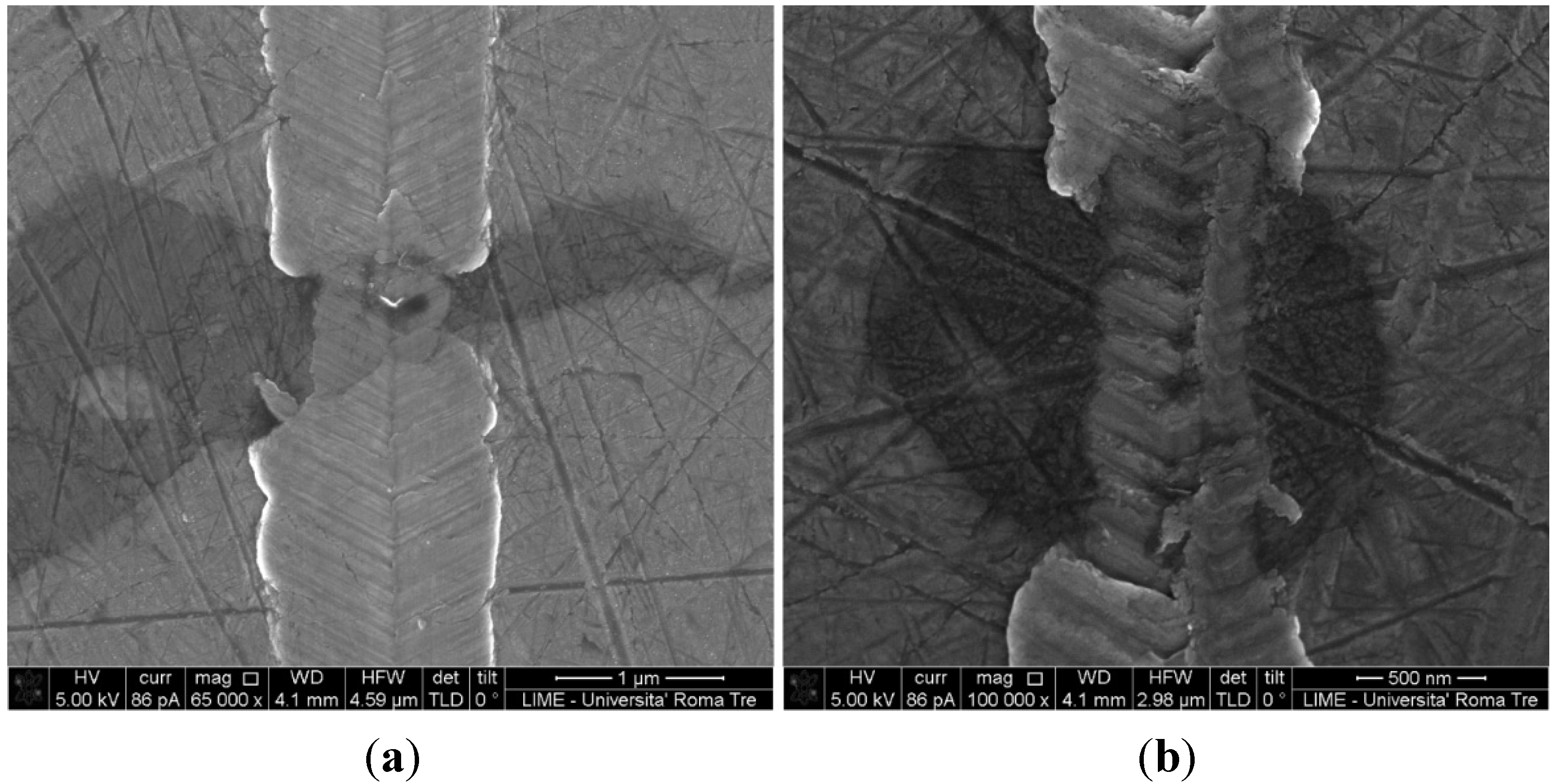
Nanoscratching was performed by means of a Berkovich nanoindenter with the aim to gain information on the wear resistance of the samples. Displacement into surface
vs. scratch distance curves were also performed, although not shown here for brevity. The results showed that the Cu-rich phases are more resistant to scratch, as a consequence of their higher hardness; this result was confirmed after SEM imaging of the scratches: the width of the scratch is significantly reduced in correspondence with the Cu-rich grains, as shown in
Figure 9, as examples, for samples 1467 and 1468. In
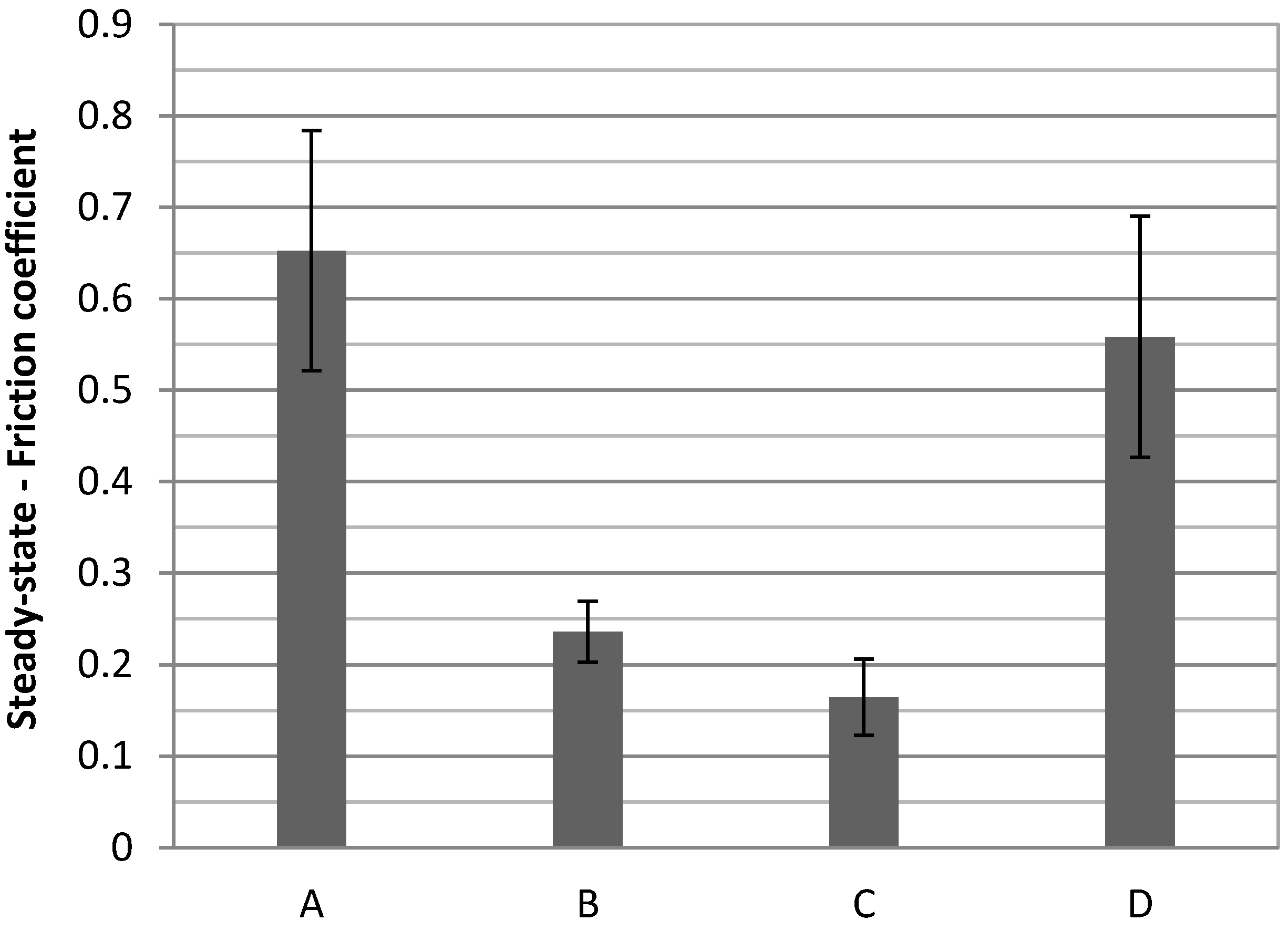
Figure 10 the histogram of the friction coefficient for all the samples is reported. It is possible to notice that the friction coefficient greatly decreases for samples treated at 100 °C (friction coeff. = 0.236 for sample 1468 and 0.164 for sample 1469), with respect to the room temperature sample (friction coeff. = 0.653). This suggests that the oxide layer that forms at this temperature might act as a solid state lubricant, greatly reducing the friction coefficient. A reduction of the friction coefficient directly involves a reduction of the surface contact stress during sliding contact, thus enhancing the scratch and wear resistance of the component. Also, the higher values of surface roughness evidenced by AFM for sample 1470 could give rise to significantly higher values of surface contact stresses during nanoscratch tests [
18].
Figure 9.
SEM micrographs of the scratches indented on samples (a) 1467 and (b) 1468.
Figure 9.
SEM micrographs of the scratches indented on samples (a) 1467 and (b) 1468.
Figure 10.
Values of the friction coefficient for all samples. A: 1467; B: 1468; C: 1469; D: 1470.
Figure 10.
Values of the friction coefficient for all samples. A: 1467; B: 1468; C: 1469; D: 1470.
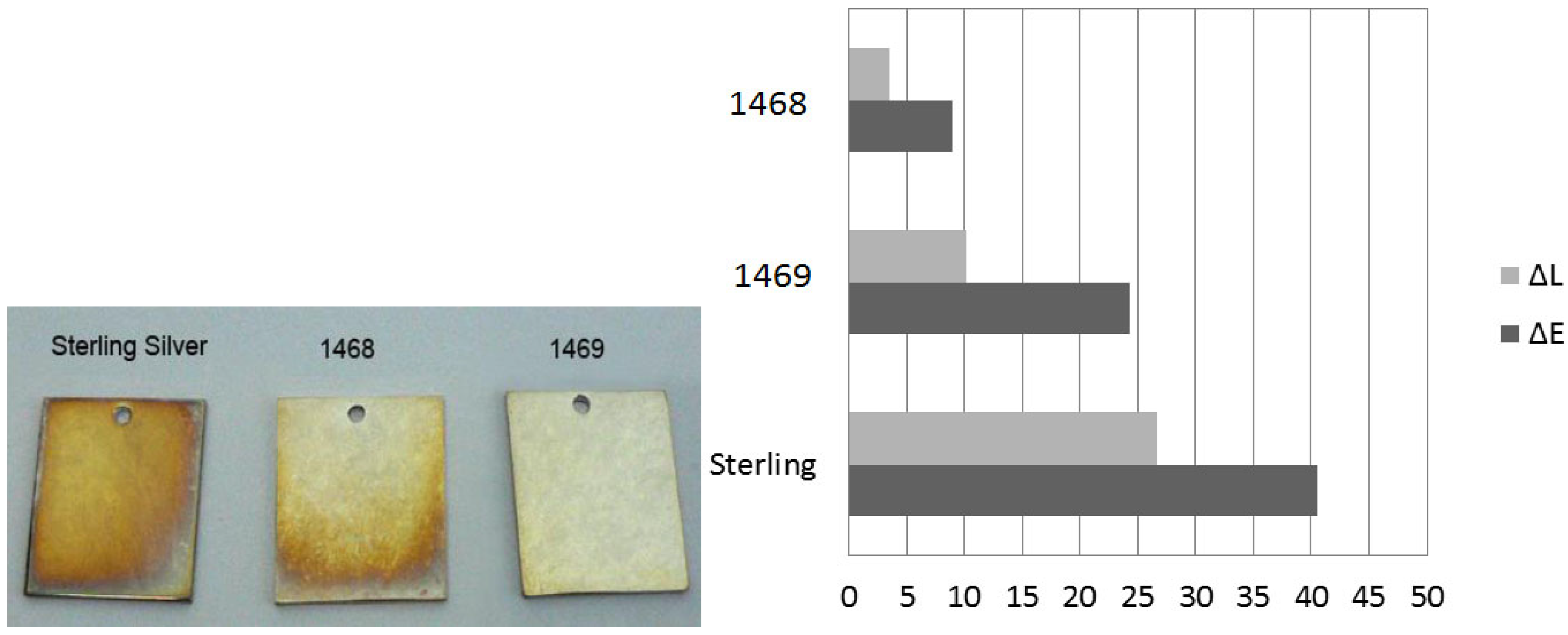
We can conclude that the addition of germanium to Sterling silver, and an opportune passivation treatment, not only improves its tarnishing and fire stain resistance, reducing the frequency of the re-polishing and increasing the time between one re-polishing treatment and the subsequent one, but it also increases the wear resistance of the alloy. This is particularly desirable since re-polishing of tarnished silver often produces wear and scratches causing the material to lose its pristine appearance.
While increasing passivation time produces a better friction coefficient, a different behavior occurs if the temperature is too high. For the sample treated at 200 °C the value of the friction coefficient rises up almost to the value of the non-treated sample (friction coeff. = 0.558). Once again this is in agreement with the formation of a brittle oxide that cracks up so that the lubrication effect between the probe and the material is lost.
3.3. Further TEM Characterization
To have a further insight on the anomalous behavior of sample 1470, SAED analysis was performed, on this sample and the results were compared with sample 1469.
The electron beam of TEM was moved along a line starting from the “bulk” material and proceeding towards the platinum protective layer; then the areas of the sample in which the diffraction pattern changed were studied. If a change in the spots pattern takes place, then a new crystalline phase is found. If the spots disappear, then an amorphous phase is encountered.
Figure 11.
Selected area electron diffraction (SAED) analysis of sample 1469, performed with TEM (120 kV, camera length 470 mm). The circles mark the zones of the diffraction patterns.
Figure 11.
Selected area electron diffraction (SAED) analysis of sample 1469, performed with TEM (120 kV, camera length 470 mm). The circles mark the zones of the diffraction patterns.
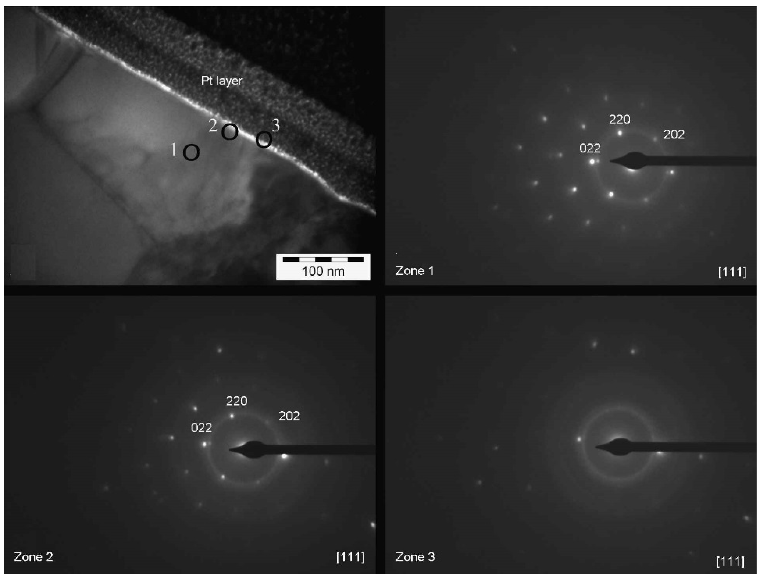
Figure 11 shows the SAED results for sample 1469. The images were acquired in three areas: inside the β-phase (zone 1), inside the oxide layer, closer to the alloy (zone 2) and inside the oxide layer, closer to the platinum protective layer (zone 3). Since there is no change in the position of the spots, but only a disappearing of the spots, then no intermediate crystallographic structure between the crystalline cell of β-phase (zone 1) and the amorphous structure of platinum layer is present. Thus, although the oxide layer is extremely thin for this kind of analysis, we can conclude that the structure of the oxide is most likely amorphous, or at least amorphous to a certain degree.
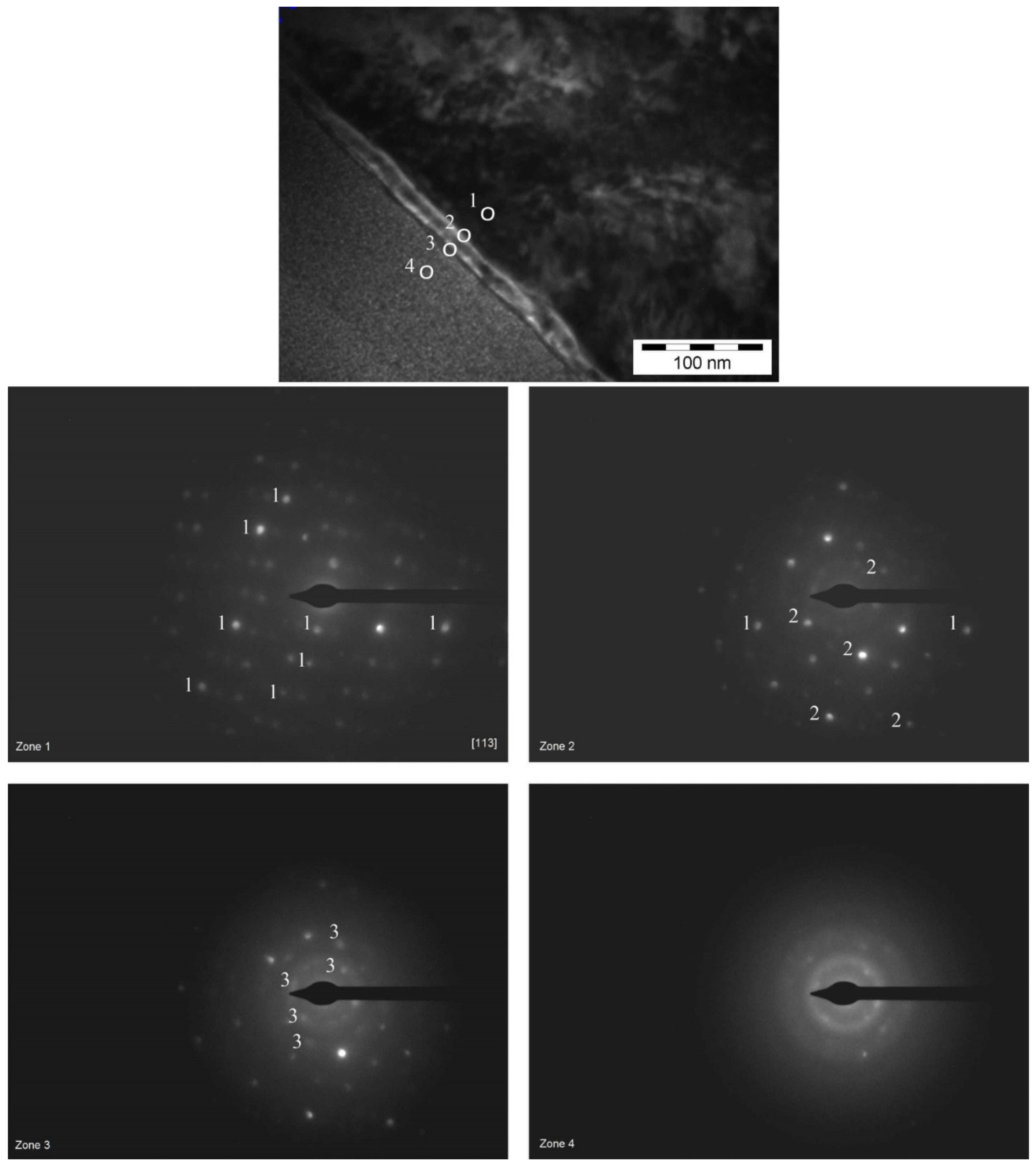
Figure 12 shows the analysis for sample 1470. In this case the analysis was performed in four different areas comprising the β-phase (zone 1), the oxide layer closer to the alloy (zone 2), the oxide layer closer to the platinum protective layer (zone 3) and the platinum layer itself (zone 4).
Figure 12.
SAED analysis of sample 1470, performed with TEM (120 kV, camera length 470 mm). The circles mark the zones of the diffraction patterns.
Figure 12.
SAED analysis of sample 1470, performed with TEM (120 kV, camera length 470 mm). The circles mark the zones of the diffraction patterns.
A change in the position of the spots is evidenced from the comparison between the four diffraction patterns. The spots marked with (1) in zone 1 tend to disappear while progressing along the path of analysis; however, some new spots appear, those marked with (2). Such patterns clearly show that there is an intermediate crystallographic structure between the cell of β-phase (zone 1) and the structure of the platinum layer (zone 4). Then, in zone 3 a third series of spots appears, which suggests that in this case part of the platinum is crystalline as well. Finally, as shown in zone 4, most of the spots disappear, leaving only the ones that appeared last (crystalline platinum mixed with amorphous platinum; platinum can be crystalline or amorphous depending on its electronic or ionic nature). We can easily conclude that, in this case, the structure of the oxide layer is crystalline.
The crystallinity of the oxide layer on sample 1470 gives a further explanation of its brittleness, thus confirming the results obtained with AFM and SEM, and of the increase of the friction coefficient observed with the nanoscratching test.
3.5. General Discussion
All samples showed a typical two phase structure, with a Cu rich second phase included in an Ag rich matrix. Sample 1467 was not heat treated and the β-phase inclusions present a lamellae spacing due to the lamination of the sample. The heat treatment relaxes the distribution of the inclusions which appear more randomly dispersed (
Figure 1).
A thin oxide layers forms in all heated samples, and it appears that the annealing improves the concentration of germanium on the surface. Preferential oxidation of germanium rather than copper is evident in sample 1469 with respect to sample 1468 and 1467.
Samples 1467, 1468, and 1469 bulk properties are almost the same and their Cu-rich grains show higher elastic modulus and hardness, in comparison with the Ag-rich matrix. Sample 1470 shows a different mechanical behavior since a significantly lower hardness is measured, and a marked reduction of the elastic modulus is observed: this has been related to the formation of a brittle oxide layer.
A passivation temperature of 100 °C and a time of 16 h are the best experimental conditions to produce a wear resistant, uniformly distributed oxide layer. A sample prepared under such parameters also proved to have the higher tarnish resistance.
Sample 1470 was treated at a significant higher temperature than samples 1468 and 1469 but for less time. In this case, however, the resulting material performed poorly, as it was covered by a thick, brittle oxide that cracked and did not provide the tarnishing protection required.


 ,
, 


