

The Electronic Structure and Optical Properties of CdGeAs2 Crystal: A DFT and HSE06 Study

1
Network Information Center, Yan’an University, Yan’an 716000, China
2
School of Physics and Electronic Information, Yan’an University, Yan’an 716000, China
3
College of Physics and Electronics Information, Yunnan Key Laboratory of Opto-Electronic Information Technology, Yunnan Normal University, Kunming 650500, China
*
Authors to whom correspondence should be addressed.
†
These authors contributed equally to this work.
Coatings 2022, 12(11), 1778; https://doi.org/10.3390/coatings12111778
Submission received: 28 October 2022
/
Revised: 14 November 2022
/
Accepted: 16 November 2022
/
Published: 21 November 2022
(This article belongs to the Topic Materials and Surface Treatment Processes Used for Engineering Applications)
Abstract
:The electronic structural and optical properties of CdGeAs2 crystals are calculated by using the Perdew–Burke–Ernzerhof (PBE) functional within generalized gradient approximation (GGA) and the Heyd–Scuseria–Ernzerhof (HSE06) functional. The results show that CdGeAs2 is an optical crystal with a direct bandgap of 0.71 eV by using the HSE06 functional method, which is closer to the experimental value. The Mulliken population and differential charge density analysis indicate that the Ge–As and Cd–As bonds have covalent properties, and that the covalent bond of Cd–As is visibly stronger than that of the Ge–As bond. The optical properties show that the CdGeAs2 crystal has strong absorption and reflection in the ultraviolet region and strong transmittance in the infrared region. The average static refractive index of CdGeAs2 is 2.96, and the static birefractive index is 0.08. The results show that CdGeAs2 is an excellent optical material of potential applications in the middle and far infrared.
1. Introduction
The CdGeAs2 crystal is a typical II-IV-V2 ternary chalcopyrite semiconductor compound, which has a wide transparent range (2.3~18 μm) [1], the highest nonlinear optical coefficient (d36 = 236 pm/V) [2], a large birefringence (ne − no ≈ 0.09) [3], and high thermal conductivity (0.04 W/(cm·K)) [4]. Therefore, the CdGeAs2 crystal can be widely used in the production of frequency-doubling and frequency-mixing infrared parametric oscillators [5]. It has broad application prospects in the military and civil fields such as optical devices [6], laser technology [7,8,9], infrared medical instruments [10], and so on. It is a middle and far infrared nonlinear optical crystal with great development prospects, which has attracted much attention at home and abroad.
Since the late 1960s, there have been many experimental studies on CdGeAs2 crystals, including photoluminescence [11], optical parametric oscillator [12], p-type CdGeAs2 luminescence and optical absorption [13], CdGeAs2 defects and doping [14,15], etc. However, compared to the experimental research, there are few theoretical studies. Most researchers focus on the electronic structure of the CdGeAs2 crystal, and the studies on the optical properties are relatively simple and incomplete. For example, Yu et al. [16] calculated the band structure, density of states, charge density, the dielectric function, and other properties of the CdGeAs2 crystal by using a pseudopotential plane wave method. The bandgap value calculated by the local density approximation (LDA) method was 0.16 eV, and the GW approximation (GWA, where G is the Green’ s function and W is the screened coulomb interaction) method was 0.35 eV. In addition, only the dielectric function is calculated in the linear optical response. Ma et al. [17] calculated the electronic structure, optical properties, and elastic properties of the CdGeAs2 crystal using the GGA–PBE and LDA methods, in which the calculated bandgap values were 0.23 eV (GGA–PBE) and 0.41 eV (LDA), and only the dielectric function and refractive index were studied in the study of optical properties. Yu et al. [18] studied the structure, electronic, and optical properties of the CdGeAs2 crystal by the HSE06 method, and the calculated bandgap value was 0.548 eV, which indeed effectively reduced the theoretical error of the bandgap. However, the optical properties of the CdGeAs2 crystal were rarely studied and analyzed. According to a significant portion of the literature, it is found that the bandgap of the crystal can be seriously underestimated by the theoretical calculation based on the GGA–PBE and LDA methods. Which is quite different from the bandgap value obtained by the experimental research (0.67 eV [19]). However, we can use some accurate hybrid functionals of exchange potentials to obtain accurate values of bandgap. The experimental studies show that optical properties are very important factors affecting the practical application of the CdGeAs2 crystal, so it is very necessary to conduct a comprehensive theoretical study on the optical properties of the CdGeAs2 crystal, which can provide an important theoretical reference for the improvement of crystal optical quality, experimental preparation, and application.
In this work, the electronic and optical properties of the CdGeAs2 crystal are calculated by the GGA–PBE [20] and HSE06 [21] methods, respectively. According to the calculated results, we can obtain more accurate electronic structures and compare them with experimental values. On the basis of calculating the dielectric function of CdGeAs2, the reflectance spectrum, the absorption spectrum, the complex refractive index, the birefringence, and the energy loss function of CdGeAs2 was calculated, and the relationship between electronic structure and optical properties were systematically studied. It has important guiding significance for the improvement of the experimental preparation and practical application of CdGeAs2.
2. Theoretical Model and Calculation Method
2.1. Theoretical Model
The CdGeAs2 crystal belongs to the II-IV-V2 chalcopyrite structure semiconductor, and its crystal structure can be regarded as the superposition of two binary cubic sphalerite crystal cells, which is equivalent to expanding the c-axis direction of sphalerite by two times. In fact, there is only one cation in the sphalerite structure, while there are two different types of cations in the ternary chalcopyrite structure, which causes the decrease in the symmetry of the chalcopyrite structure system. In general, the II-V atomic bond lengths (dII-V) and the IV-V atomic bond lengths (dIV-V) are not equal, resulting in two different structural deformations: The first deformation is a change in the occupation of anions, with the anion having an inner coordinate u = 0.25 for sphalerite and u = 0.25 + (d2II-V − d2IV-V)/a2 for chalcopyrite, where a is the lattice constant along the x or y directions [22]. The second deformation is that the lattice constant (c) along the z direction is not equal to 2a, which means that c/a is not equal to 2. For the II-IV-V2 chalcopyrite structure, u = 0.214~0.304, c/a = 1.769~2.016 in most cases, and the structure parameters of the CdGeAs2 crystal are also within this boundary range. In the crystal structure of CdGeAs2, the Cd, Ge, and As atoms form a tetrahedron, the anion As3− is located in the center of the tetrahedron, and the cations Cd and Ge occupy the four top angles of the tetrahedron. In each layer, the cations Cd and Ge are arranged in a certain order [23]. The structural model of CdGeAs2 is shown in Figure 1.
2.2. Calculation Method
In this work, we calculated the structural optimization and performance of the crystal using the Vienna ab-initio Simulation Package (VASP) [24]. The GGA–PBE method is used to accurately calculate the total energy and exchange-related interactions. We use the HSE06 method to avoid the underestimation of bandgap values and the overestimation of optical responses in standard density functional theory (DFT) [25] calculations. The valence electrons of Cd, Ge, and As are 4d105s2, 4s24p2, and 4s24p2, respectively. In the electron self-consistent iterative cycle, the criterion for convergence is 1 × 10⁻⁵ eV/Å for the total energy and 1 × 10⁻⁶ eV for the atomic relaxation. The truncation energy is set to 520 eV. The k-points grid is set to 6 × 6 × 4 according to the Monkhorst–Pack scheme, which can ensure that the system always converges well.
3. Results and Discussion
3.1. Geometric Optimization Results
In order to obtain reasonable calculation results, a stable crystal structure is necessary. The lattice parameters of the stable structure are obtained according to the principle of minimizing the total cell energy, and the obtained crystal cell parameters are shown in Table 1. The lattice constants of the stable structure of the CdGeAs2 crystal are as follows: a = b = 6.041 Å, c/a = 1.887, u = 0.278. The optimized lattice constant a is close to the experimental value of 5.94 [26], the relative error of both a and c values is ~1.70%, and the relative error of the u value is 0.4%. Due to the fact that the optimized crystal is an ideal crystal, the zero-point motion and thermal effect are not considered, so there is a certain error with the experimental value.
3.2. Electronic Structure
The band structure of CdGeAs2, calculated by the GGA–PBE and HSE06 methods, are shown in Figure 2, and the Fermi level (Ef) is set to zero. These particular points on the x-axis represent points of high symmetry in the Brillouin zone (BZ). For the quadrilateral structure of CdGeAs2, Z = (0.3, 0.3, 0.3), Γ = (0, 0, 0), X = (0.3, 0, 0), P = (0.3, −0.3, 0.3), and N = (0.3, −0.3, 0). The characteristic energy values of the top of the valence band (EV) and the bottom of the conduction band (EC) in the BZ of CdGeAs2 are shown in Table 2. It can be seen from the values in the table that the top of the valence band (VBM) and the bottom of the conduction band (CBM) are both at the Γ point. Therefore, CdGeAs2 is a direct bandgap semiconductor material. The bandgap values (Eg) of CdGeAs2 calculated using the GGA–PBE and HSE06 methods are shown in Table 3 and compared with the experimental value. The Eg calculated by the GGA–PBE method is 0.079 eV, and the Eg calculated using the HSE06 method is 0.710 eV. Compared with the experimental values (0.67 eV [18] and 0.53 eV [27]), the average relative error calculated by the GGA–PBE method is 86.65%, which seriously underestimates the bandgap value, while the average relative error calculated by the HSE06 method is 19.97%, which is closer to the experimental value. The relevant values are listed in Table 3. When the Eg is calculated by the GGA method, the self-interaction of electrons does not cancel completely in the exchange-correlation potential, and its eigenfunction is discontinuous, so the GGA method will underestimate Eg. When the calculation does not include the spin–orbit interactions, the three lower conduction band (CB) states at the Γ point are Γ1, Γ3, and Γ2. The energy splitting value between Γ2 and Γ3 is 0.49 eV, which is very close to the 0.46 eV calculated by Limpijumnong et al. [28]. At point Γ, the top of the valence band (VB) consists of two symmetric levels Γ4 and Γ5, the latter being a double degenerate level. Due to the crystal field (CF), the non-degenerate Γ4 and double-degenerate Γ5 in the chalcopyrite structure originate from the Γ15 level of the zinc–blende structure [29]. Therefore, the crystal field splitting can be expressed as ΔCF = ε (Γ5) − ε (Γ4). The calculated ΔCF value of CdGeAs2 is 0.227 eV, which is very close to the experimental value (0.21 eV) [30].
We analyze the distribution of electrons per atomic orbital by calculating the total density of states (TDOSs) and partial density of states (PDOSs). Figure 3 shows the TDOSs and PDOSs of CdGeAs2 calculated using the GGA–PBE method and the HSE06 method. As can be seen from the figure, the VB of CdGeAs2 can be divided into three regions: In the lower VB (−13~−11 eV), it is mainly composed of As-4s states, with a small amount of Ge-4p and Ge-4s orbital hybridization. In the intermediate VB (−10~−6 eV), it is mainly composed of Ge-4s and Cd-4d electronic states. The higher VB (−5~0 eV) is mainly derived from the As-4p and Ge-4p states. The CB is mainly composed of the As-4s, As-4p, Ge-4p, and Ge-4s orbitals. The density of states (DOSs) near the VBM and the CBM are mainly derived from As atoms, as shown in Figure 3. In the experiment, the change of As content will change the bandgap of the single crystal, and then affect the optical transmittance. Therefore, the content of As can be increased appropriately when preparing a CdGeAs2 single crystal.
3.3. Mulliken Charge Population Analysis
We computed the Mulliken population analysis, which allows us to understand the interaction and bonding between atoms. The Mulliken charge, bond lengths, and bond lattice numbers of CdGeAs2 crystals calculated using the GGA–PBE and HSE06 methods are shown in Table 4. From the calculation results, it can be seen that the charge transfer of the CdGeAs2 compounds is from the Cd and Ge atoms into the As atoms. Taking the calculation results of the HSE06 method as an example: the Cd and Ge atoms carry positive charges of 0.19 and 0.13, respectively. The Cd and Ge atoms are very capable of losing electrons, while the As atoms carry negative charges of 0.16 and are very capable of gaining electrons. The bond characteristics (ionic bonds or covalent) can be assessed and determined using overlapping populations. In general, a zero number of the chemical bond population indicates an ideal ionic bond, while a positive value is proportional to the covalency of the bond. In Table 4, the populations of As atoms with Cd atoms and Ge atoms are 0.67 and 0.26, respectively, which confirmed that the covalency of the Cd–As bond and that the Ge–As bond of CdGeAs2 compounds is weak, as well as that the covalency of the Cd–As bond is higher than that of the Ge–As bond.
3.4. The Differential Charge Density
Figure 4 shows the differential charge density of CdGeAs2 to visualize the bond properties. Figure 4a shows the 3D differential charge density of CdGeAs2, where green represents electron loss and yellow represents electron gain. It can be seen that electrons accumulate near the As atom, and that the Cd atom is surrounded by green, indicating that it has a strong ability to lose electrons. The Cd–As atoms form strong chemical bonds with each other, while the Ge–As atoms form weak bonds with each other. Figure 4b shows the 2D plan differential charge density of CdGeAs2. Figure 3 shows that the intermediate region (−10~−6 eV) is mainly derived from the Cd-4d states and is thus strongly localized around the Cd atom. As can be seen from Figure 4b, there is an obvious electron density overlap between the As atom, the Ge atom, and the Cd atom, which indicates that the bonds Ge–As and Cd–As have covalent properties. The density lines in the 2D differential charge map indicate that the Cd–As bond has stronger covalent properties than the Ge–As bond. This result is consistent with the Mulliken population analysis.
3.5. Optical Properties
Generally, the complex dielectric function can be used to express the macroscopic optical properties of solids [31]:
where ε1(ω) is the real part, and ε2(ω) is the imaginary part. The imaginary part ε2(ω) can be calculated according to the following formula:
where C and V represent CB and VB, corresponding to the intrinsic energy EC(k) and EV(k) of the CB and VB, respectively. MCV stands for transition matrix element, ω is the electromagnetic wave frequency, and k is the electron wave vector. Real ε1(ω) is derived from imaginary ε2(ω) using the Kramers–Krönig relation:
where P is the principal value of the integral. The imaginary and real parts of the dielectric function can be used to calculate other optical properties, such as refractive index n(ω), reflectivity R(ω), conductivity function σ(ω), and energy loss spectrum L(ω). The formula is as follows:
In this paper, the GGA–PBE and HSE06 methods are used to calculate the dielectric function of CdGeAs2 material. Due to the symmetry of the crystal, the dielectric function is decomposed into two components. E⊥c is the electric field along the x and y directions (the electric field perpendicular to the optical axis), and E//c corresponds to the z direction (the electric field parallel to the optical axis). Figure 5a,c show the real part ε1(ω) of the dielectric function calculated by the GGA–PBE and HSE06 methods, respectively. When ε1(ω) photon energy tends to 0, the average static permittivity (ε1ave (0)) of CdGeAs2 calculated using the GGA–PBE and HSE06 methods are 18.42 and 16.57, respectively. The experimental value of the dielectric function is 15.4 [32], and the relative errors are 19.61% (GGA–PBE) and 7.59% (HSE06). Therefore, the results calculated by the HSE06 method are closer to the experimental value.
Figure 5b,d show the imaginary part ε2(ω) of the dielectric function calculated by the GGA–PBE and HSE06 methods, respectively. ε2(ω) determines the linear response of the light field. The basic absorption edges, calculated by the GGA–PBE and HSE06 methods, are 0.09 eV and 0.72 eV, respectively, which is connected with the electron transition from the VBM to the CBM. The dielectric spectrum can be divided into four regions: 0~0.6 eV and >17 eV are the transparent areas, 0.6~10 eV is the absorption area, 10~17 eV is the reflex area. In the region above the absorption edge, there are two main dielectric peaks, namely P1 and P2 in ε2(ω). The photon energies corresponding to the dielectric peaks calculated by GGA–PBE are 1.94 eV and 4.81 eV, respectively, while those calculated by HSE06 are 2.65 eV and 5.61 eV, respectively. As can be seen from Figure 3, peak P1 is mainly derived from the electronic transition of the As-4p states between the CB and VB, while peak P2 is generated by the electronic transition of the As-4p and Ge-4p orbitals between the CB and VB.
In this paper, the GGA–PBE and HSE06 methods are used to calculate the reflection and absorption spectra of CdGeAs2 crystals, as shown in Figure 6. The CdGeAs2 reflectance spectrum obtained according to Equation (5) is shown in Figure 6a,b. The reflectance shows obvious anisotropy along different directions. Due to the band transition of CdGeAs2, the reflectance is proportional to the energy change. The reflectance reaches its maximum value around 10.0 eV. With increasing energy, the reflectance rapidly decreases to 0. In conclusion, the CdGeAs2 crystal has low reflectance in the infrared band.
The absorption spectrum of CdGeAs2 obtained according to Equation (6) is shown in Figure 6c. The absorption calculated by the PBE and HSE06 methods starts at about 0.09 eV and 0.72 eV, respectively, which corresponds to the bandgap value of the material. The strongest absorption peak calculated by the GGA–PBE method appears at 6.82 eV, and the strongest absorption peak calculated by the HSE06 method appears at 7.75 eV.
The refractive index and the extinction coefficient of CdGeAs2, calculated by the GGA–PBE and HSE06 methods, are shown in Figure 7. The propagation speed of light wave in CdGeAs2 determines the refractive index (n), and the attenuation of light wave determines the extinction coefficient (k). The average static refractive index calculated by the GGA–PBE method and the HSE06 method are 4.67 and 2.96, respectively. The extinction coefficients calculated by the GGA–PBE method have peaks at 2.07 eV and 4.95 eV. The peak values calculated by the HSE06 method were 2.79 eV and 5.93 eV, which is consistent with ε2(ω).
The birefringence (Δn) of the CdGeAs2 crystal calculated using the GGA–PBE and HSE06 methods is shown in Figure 8. The birefringence is expressed as the difference between two or three main refractive indices () in heterogeneous bodies. The birefringence is an important physical quantity in measuring nonlinear crystal properties. The most suitable birefringence range of mid-infrared nonlinear optical crystal is 0.04 < Δn < 0.1 [33]. According to Figure 8a, the static birefringence of CdGeAs2 calculated using the GGA–PBE method is 0.11, which reaches the maximum value of 0.54 at 4.09 eV. As can be seen from Figure 8b, the static birefringence of CdGeAs2 calculated using the HSE06 method is 0.08, which reaches the maximum value of 0.33 at 7.59 eV. At the wavelength of 10 μm, the experimental value of birefringence is 0.0864 [34]. The relative errors are 27.31% (GGA–PBE) and 7.41% (HSE06), so the result calculated by the HSE06 method is closer to the experimental value. By comparing the results calculated using the GGA–PBE and HSE06 methods, it is found that the bandgap of the CdGeAs2 crystal is underestimated by the GGA–PBE method, which leads to the increase in the average static refractive index and birefringence in the mid-far infrared region.
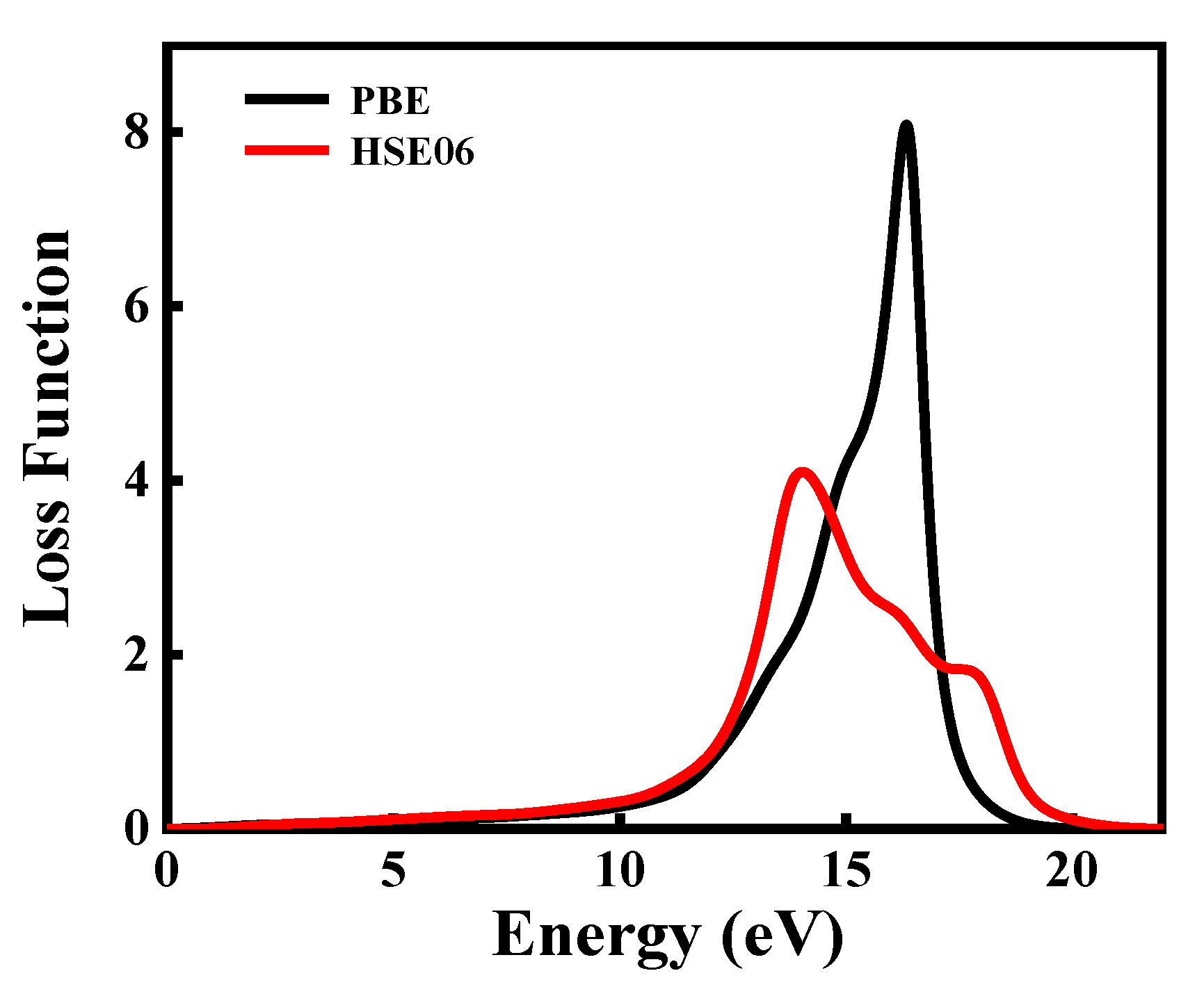
According to Equation (7), the energy loss function of CdGeAs2 is calculated, which describes the energy loss of the electrons when they pass through the medium. The energy loss spectrum of CdGeAs2 is shown in Figure 9. The maximum energy loss peak at 16.36 eV is calculated by the GGA–PBE method, and its value is 8.09. The result obtained by the HSE06 shows that the maximum energy loss occurs at 14.06 eV, and its value is 4.08. In addition, it can be concluded from the band structure and the DOS analysis that the highest peak comes from the transition of the As-4s, Ge-4s, and Ge-4p orbitals from the VB to the CB.
4. Conclusions
In this work, the electronic structure and optical properties of the CdGeAs2 crystal are calculated using GGA–PBE and HSE06 methods. The results show that the relative error of the bandgap value calculated by GGA–PBE method is large, while the result calculated by the HSE06 method is closer to the experimental value. The calculation results of the DOSs show that the VBM is mainly composed of As-4p and Ge-4p states, and that the CBM is mainly composed of the orbitals of As-4s, As-4p, Ge-4s, and Ge-4p. The Mulliken population analysis and differential charge density results show that the bonds Ge–As and Cd–As are covalent. Moreover, the covalency of the Cd–As bond is higher than that of the Ge–As bond. In addition, we systematically calculate the optical properties of CdGeAs2. The relative errors of average static permittivity calculated using GGA–PBE and HSE06 are 19.61% and 7.59%, respectively, and the relative errors of static birefringence are 27.31% and 7.41%, respectively. The results of the optical properties show that the CdGeAs2 crystal has strong absorption and reflection in the ultraviolet region, along with strong transmission and excellent birefringence in the infrared region. In summary, the HSE06 method is more suitable for calculating the electronic structure and optical properties of the CdGeAs2 crystal. Meanwhile, the theoretical calculation results prove that the CdGeAs2 crystal is an excellent medium and far infrared optical crystal material, and the calculation results provide an important theoretical reference for the improvement of crystal optical quality, experimental preparation, and its application.
Author Contributions
F.Z. and W.Z. supervised the research. J.N. and S.X. calculated a series of properties of the material and wrote the first draft. B.Z. and Q.W. analyzed the data and revised the paper. All authors have read and agreed to the published version of the manuscript.
Funding
This research was funded by the National Natural Science Foundation of China (Grant No. 62264015, 52262042), the National Science Foundation of Shaanxi Province, China (2021JQ-635), the Scientific Research Program of Yan’an University (YDQ2020-08), and the Scientific and Technological Innovation Team (2017CXTD-01).
Institutional Review Board Statement
This work does not involve humans or animals.
Informed Consent Statement
Not applicable.
Data Availability Statement
All data are presented in the form of charts in the article.
Conflicts of Interest
The authors declare no conflict of interest.
References
- Huang, W.; Zhao, B.; Zhu, S.; He, Z.; Chen, B.; Yu, Y. Vibrational modes of chalcopyrite CdGeAs2 crystal. Mater. Res. Bull. 2016, 81, 107–113. [Google Scholar] [CrossRef]
- Huang, W.; Zhao, B.; Zhu, S.; He, Z.; Chen, B.; Zhen, Z.; Pu, Y. Correlation between dislocation etch pits, carrier concentration and optical absorption in CdGeAs2 grown by modified Vertical Bridgman method. J. Alloys Compd. 2016, 656, 818–824. [Google Scholar] [CrossRef]
- Pu, Y.; Zhu, S.; Zhao, B.; He, Z.; Chen, B.; Huang, W. Growth and characterization of Cr-doped CdGeAs2 crystal. J. Cryst. Growth 2017, 467, 150–154. [Google Scholar] [CrossRef]
- Li, J.; Zhu, S.; Zhao, B.; He, Z.; Chen, B. XPS Analysis and Determination of Surface Damage Layer of CdGeAs2 Single Crystal. Rare Met. Mater. Eng. 2015, 44, 844–847. [Google Scholar]
- Vodopyanova, K.L.; Knippels, G.M.H.; van der Meer, A.F.G.; Maffetonec, J.P.; Zwieback, I. Optical parametric generation in CGA crystal. Opt. Commun. 2002, 202, 205–208. [Google Scholar] [CrossRef] [Green Version]
- Yu, Y.; Zhao, B.; Zhu, S.; Gao, T.; Hou, H. Ab initio vibrational and dielectric properties of chalcopyrite CdGeAs2. Solid State Sci. 2011, 13, 422–426. [Google Scholar] [CrossRef]
- Mei, D.; Jiang, J.; Liang, F.; Zhang, S.; Wu, Y.; Sun, C.; Xue, D.; Lin, Z. Design and Synthesis of Nonlinear Optical Material with Wide Band Gap: From SrB4O7 to BaAl4S7. J. Mater. Chem. C 2018, 6, 2684–2689. [Google Scholar] [CrossRef]
- Lin, Z.; Jiang, X.; Kang, L.; Gong, P.; Luo, S.; Lee, M. First-principles materials applications and design of nonlinear optical crystals. J. Phys. D 2014, 47, 253001. [Google Scholar] [CrossRef] [Green Version]
- Bera, T.K.; Song, J.H.; Freeman, A.J.; Jang, J.I.; Ketterson, J.B.; Kanatzidis, M.G. Soluble Direct-Band-Gap Semiconductors LiAsS2 and NaAsS2: Large Electronic Structure Effects from Weak As···S Interactions and Strong Nonlinear Optical Response. Angew. Chem. Int. Ed. 2008, 47, 7828–7832. [Google Scholar] [CrossRef]
- Lei, Y.; Yu, M.; Li, J.; Wu, J.; Chen, B.; Yu, Y.; Huang, W.; He, Z. Synthesis, growth and mechanical properties of mid-infrared nonlinear optical crystal CdGeAs2. J. Cryst. Growth 2021, 562, 126060. [Google Scholar] [CrossRef]
- Bai, L.; Xu, C.; Nagashio, K.; Yang, C.; Feigelson, R.S.; Schunemann, P.G.; Giles, N.C. Photoluminescence of n-type CdGeAs2. J. Phys. Condens. Matter. 2005, 17, 5687–5696. [Google Scholar] [CrossRef] [PubMed]
- Huang, W.; Zhao, B.; Zhu, S.; He, Z.; Chen, B.; Li, J.; Yu, Y.; Tang, J.; Liu, W. Effect of thermal annealing on the optical properties of CdGeAs2 wafers. J. Cryst. Growth 2013, 362, 291–295. [Google Scholar] [CrossRef]
- Bai, L.; Poston, J.A.; Schunemann, P.G.; Nagashio, K.; Feigelson, R.S.; Giles, N.C. Luminescence and optical absorption study of p-type CdGeAs2. J. Phys. Condens. Matter. 2004, 16, 1279–1286. [Google Scholar] [CrossRef]
- Blanco, M.A.; Costales, A.; Luaña, V.; Pandey, R. Theoretical study of the group-IV antisite acceptor defects in CdGeAs2. Appl. Phys. Lett. 2004, 85, 4376–4378. [Google Scholar] [CrossRef] [Green Version]
- Garces, N.Y.; Giles, N.C.; Halliburton, L.E.; Nagashio, K.; Feigelson, R.S.; Schunemann, P.G. Electron paramagnetic resonance of Cr2+ and Cr4+ ions in CdGeAs2 crystals. J. Appl. Phys. 2003, 94, 7567–7570. [Google Scholar] [CrossRef]
- Yu, Y.; Zhao, B.; Zhu, S.; Gao, T.; Hou, H.; He, Z. Ab initio study of the linear and nonlinear optical properties of chalcopyrite CdGeAs2. J Solid State Chem. 2012, 185, 264–270. [Google Scholar] [CrossRef]
- Ma, C.G.; Krasnenko, V.; Brik, M.G. Effects of composition on the properties of mixed CdSi1-xGexAs2 chalcopyrites as explored by the first-principles calculations. Mater. Des. 2017, 126, 250–258. [Google Scholar] [CrossRef]
- Yu, M.; Xiao, X.; Xiong, Z.; Li, J.; Liu, X.; Huang, W.; Chen, B.; He, Z. Structural, electronic and optical properties of CdGeAs2 with hybrid density functional (HSE06). Mater. Today Commun. 2022, 31, 103276. [Google Scholar] [CrossRef]
- Bai, L.; Schunemann, P.G.; Pollak, T.M.; Giles, N.C. Luminescence study of donors and acceptors in CdGeAs2. Opt. Mater. 2004, 26, 501–505. [Google Scholar] [CrossRef]
- Ernzerhof, M.; Scuseria, G.E. Assessment of the Perdew–Burke–Ernzerhof exchange-correlation functional. J. Chem. Phys. 1999, 110, 5029–5036. [Google Scholar] [CrossRef] [Green Version]
- Moussa, J.E.; Schultz, P.A.; Chelikowsky, J.R. Analysis of the Heyd-Scuseria-Ernzerhof density functional parameter space. J. Chem. Phys. 2012, 136, 204117. [Google Scholar] [CrossRef] [PubMed]
- Jaffe, J.E.; Zunger, A. Theory of the band-gap anomaly in ABC2 chalcopyrite semiconductors. Phys. Rev. B 1984, 29, 1882–1906. [Google Scholar] [CrossRef] [Green Version]
- Marenkin, S.F.; Novotortsev, V.M.; Palkina, K.K.; Mikhailov, S.G.; Kalinnikov, V.T. Preparation and structure of CdGeAs2 crystals. Inorg. Mater. 2004, 40, 135–137. [Google Scholar] [CrossRef]
- Hafner, J. Ab-Initio Simulations of Materials Using VASP: Density-Functional Theory and Beyond. J Comput Chem. 2008, 29, 2044–2078. [Google Scholar] [CrossRef]
- Tomas, B.; Jurgen, H.; Sebastien, L.; Janos, G.A. Improved Description of the Structure of Molecular and Layered Crystals: Ab Initio DFT Calculations with van der Waals Corrections. J. Phys. Chem. A 2010, 114, 11814–11824. [Google Scholar]
- Abrahams, S.C.; Bernstein, J.L. Piezoelectric nonlinear optic CuGaSe2 and CdGeAs2: Crystal structure, chalcopyrite microhardness, and sublattice distortion. J. Chem. Phys. 1974, 61, 1140–1146. [Google Scholar] [CrossRef]
- Isomura, S.; Takahashi, S.; Masumoto, K. Electrical and optical properties of CdGeAs2. J. Appl. Phys. 1977, 16, 1723. [Google Scholar] [CrossRef]
- Limpijumnong, S.; Lambrecht, W.R.L. Band structure of CdGeAs2 near the fundamental gap. Phys. Rev. B. 2002, 65, 165204. [Google Scholar] [CrossRef]
- El Moctar, C.O.; Kambas, K.; Marsillac, S.; Anagnostopoulos, A.; Bernede, J.C.; Benchouck, K. Optical properties of CuAlX2 (X=Se, Te) thin films obtained by annealing of copper, aluminum and chalcogen layers sequentially deposited. Thin Solid Film. 2000, 371, 195–200. [Google Scholar] [CrossRef]
- Polygalov, Y.I.; Poplavnoi, A.S. Energy band sturcture of CdSnAs2 and CdGeAs2. Russ. Phys. J. 1981, 24, 1139–1142. [Google Scholar]
- Tauc, J. Optical properties and electronic structure of amorphous Ge and Si. Mat. Res. Bull. 1968, 3, 37–46. [Google Scholar] [CrossRef]
- Pandey, R.; Ohmer, M.; Gale, J. A theoretical study of native acceptors in CdGeAs2. J. Phys. Condens. Matter 1998, 10, 5525–5533. [Google Scholar] [CrossRef]
- Kang, L.; Zhou, M.; Yao, J.; Lin, Z.; Wu, Y.; Chen, C. Metal Thiophosphates with Good Mid-Infrared Nonlinear Optical Performances: A First-Principles Prediction and Analysis. J. Am. Chem. Soc. 2015, 137, 13049–13059. [Google Scholar] [CrossRef] [PubMed]
- Boyd, G.; Buehler, E.; Storz, F.; Wernick, J. Linear and nonlinear optical properties of ternary AIIBIVC2V chalcopyrite semiconductors. IEEE J. Quantum Electron. 1972, 8, 419–426. [Google Scholar] [CrossRef]
Figure 1.
The structural model of CdGeAs2 (orange sphere is Cd atom, blue sphere is Ge atom, pink sphere is As atom).
Figure 1.
The structural model of CdGeAs2 (orange sphere is Cd atom, blue sphere is Ge atom, pink sphere is As atom).

Figure 2.
The band structures of CdGeAs2. (a) GGA–PBE, (b) HSE06.
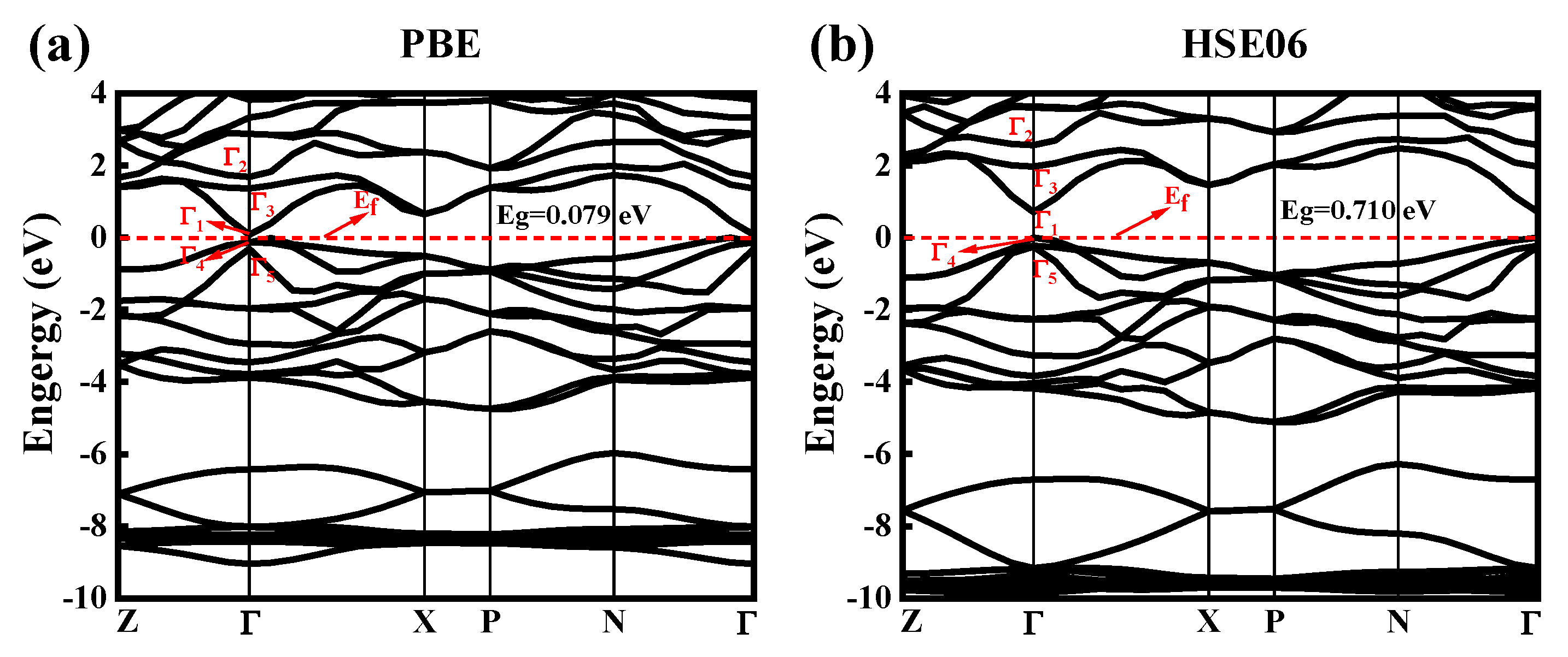
Figure 3.
The total and partial density of states of CdGeAs2. (a) GGA–PBE, (b) HSE06.
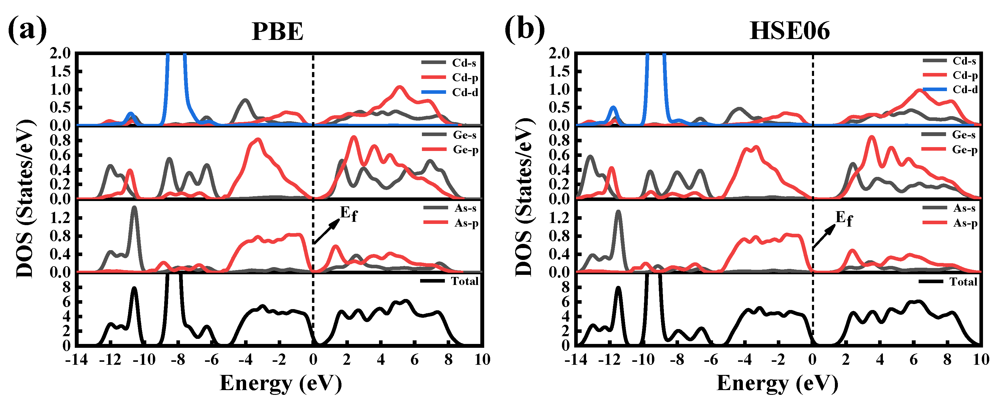
Figure 4.
The differential charge density of CdGeAs2. (a) 3D, (b) 2D.
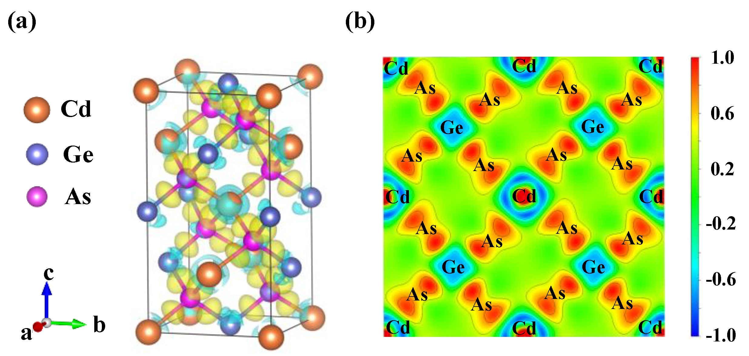
Figure 5.
(a) The real part and (b) the imaginary part of the dielectric function of CdGeAs2 of GGA–PBE; (c) the real part and (d) the imaginary part of the dielectric function of CdGeAs2 of HSE06.
Figure 5.
(a) The real part and (b) the imaginary part of the dielectric function of CdGeAs2 of GGA–PBE; (c) the real part and (d) the imaginary part of the dielectric function of CdGeAs2 of HSE06.
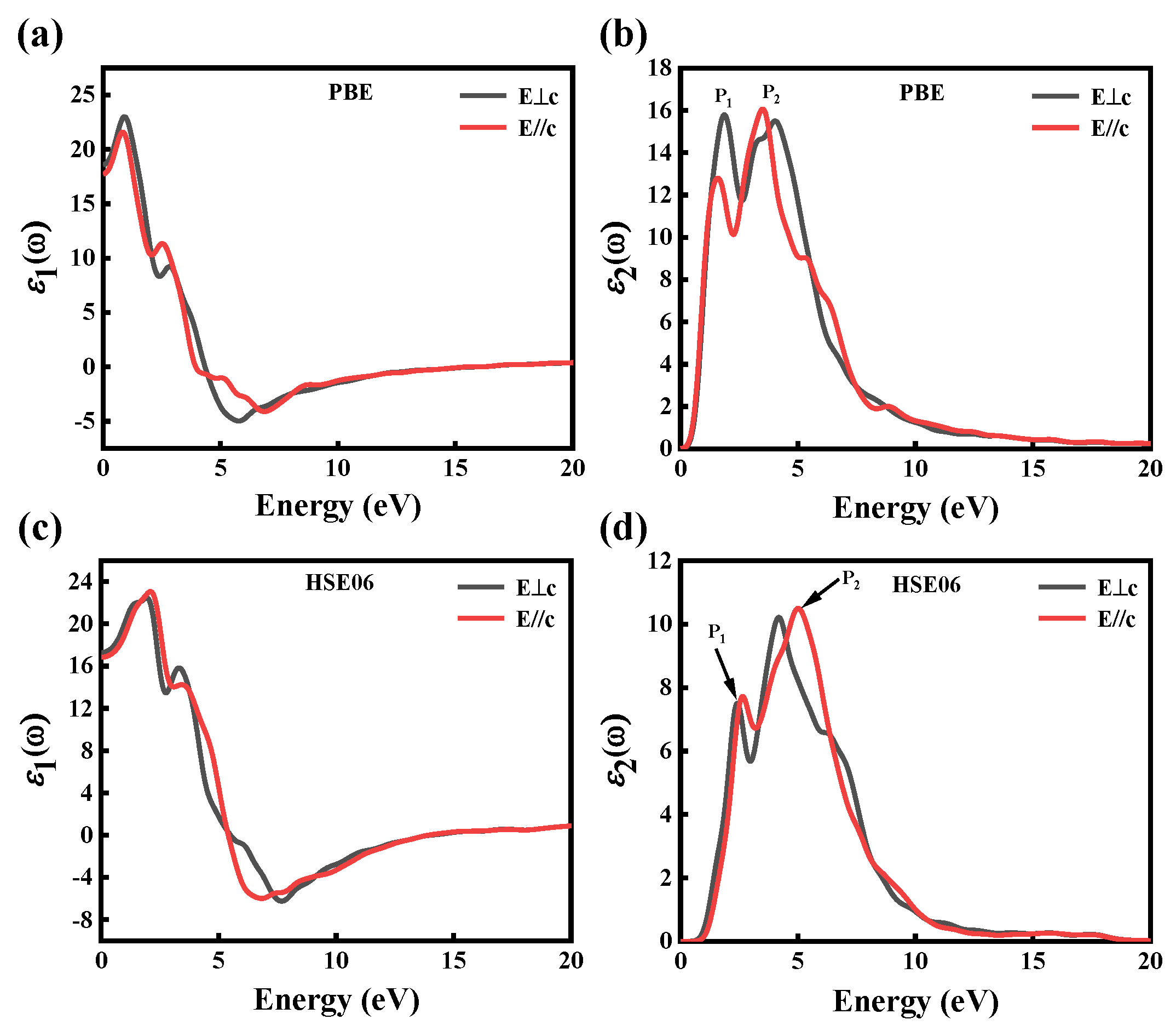
Figure 6.
(a,b) The reflectance spectrum and (c) the absorption spectrum of CdGeAs2.
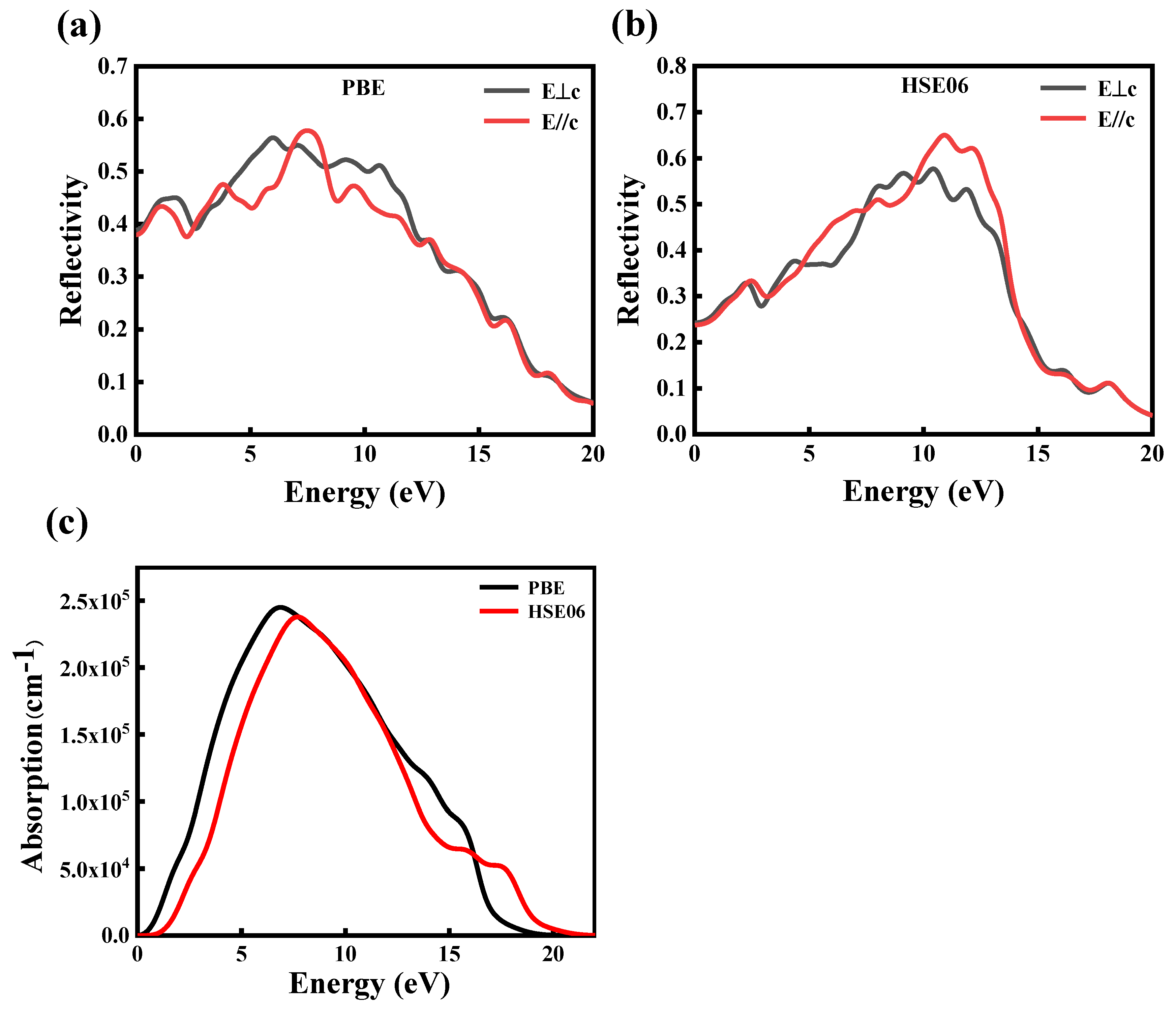
Figure 7.
The complex refractive index of CdGeAs2.

Figure 8.
The birefringence of CdGeAs2. (a) GGA–PBE, (b) HSE06.
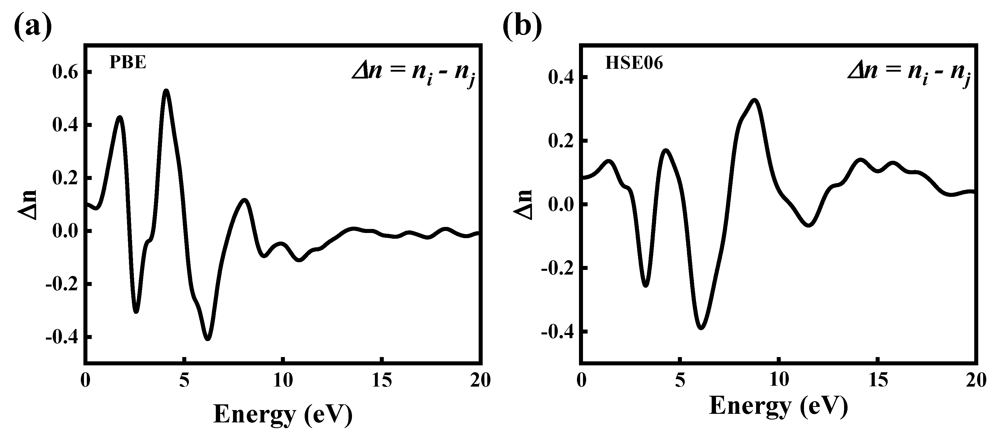
Figure 9.
The energy loss function of CdGeAs2.

Table 1.
The structural optimization results of CdGeAs2.
| Parameter | This Work | Experimental Value [26] | Relative Error |
|---|---|---|---|
| a = b/Å | 6.041 | 5.94 | 1.7% |
| c/Å | 11.407 | 11.22 | 1.7% |
| u | 0.278 | 0.279 | 0.4% |
| α = β = γ (°) | 90 | - | - |
Table 2.
The characteristic energy values of EV and EC in the BZ of CdGeAs2.
| Method | Parameter | Z | Γ | X | P | N |
|---|---|---|---|---|---|---|
| GGA–PBE | EV (eV) | 1.400 | 0.079 | 0.650 | 1.390 | 1.730 |
| EC (eV) | −0.875 | 0 | −0.509 | −0.891 | −0.580 | |
| HSE06 | EV (eV) | 2.120 | 0.710 | 1.450 | 2.040 | 2.480 |
| EC (eV) | −1.110 | 0 | −0.686 | −1.050 | −0.730 |
Table 3.
The Eg of CdGeAs2 calculated by GGA–PBE and HSE06 methods.
| Method | This Work (eV) | Experimental Value (eV) [18,27] | Mean Relative Error |
|---|---|---|---|
| PBE | 0.079 | 0.67 or 0.53 | 86.65 % |
| HSE06 | 0.710 | 0.67 or 0.53 | 19.97% |
Table 4.
The population analysis of CdGeAs2.
| Methods | Atom | s | p | d | Total | Charge | Bond | Length (Å) | Population |
|---|---|---|---|---|---|---|---|---|---|
| PBE | Cd | 0.95 | 1.08 | 9.97 | 12.00 | −0.00 | Cd–As | 2.47100 | 0.27 |
| Ge | 1.17 | 2.36 | 0 | 3.53 | 0.47 | Ge–As | 2.67279 | 0.04 | |
| As | 1.67 | 3.56 | 0 | 5.23 | −0.23 | - | - | - | |
| HSE06 | Cd | 0.78 | 1.06 | 9.97 | 11.81 | 0.19 | Cd–As | 2.46677 | 0.67 |
| Ge | 1.53 | 2.34 | 0 | 3.87 | 0.13 | Ge–As | 2.68291 | 0.26 | |
| As | 1.43 | 3.73 | 0 | 5.16 | −0.16 | - | - | - |
Publisher’s Note: MDPI stays neutral with regard to jurisdictional claims in published maps and institutional affiliations. |
© 2022 by the authors. Licensee MDPI, Basel, Switzerland. This article is an open access article distributed under the terms and conditions of the Creative Commons Attribution (CC BY) license (https://creativecommons.org/licenses/by/4.0/).
Share and Cite
MDPI and ACS Style
Xue, S.; Ning, J.; Zhang, B.; Wu, Q.; Zhang, F.; Zhang, W. The Electronic Structure and Optical Properties of CdGeAs2 Crystal: A DFT and HSE06 Study. Coatings 2022, 12, 1778. https://doi.org/10.3390/coatings12111778
AMA Style
Xue S, Ning J, Zhang B, Wu Q, Zhang F, Zhang W. The Electronic Structure and Optical Properties of CdGeAs2 Crystal: A DFT and HSE06 Study. Coatings. 2022; 12(11):1778. https://doi.org/10.3390/coatings12111778
Chicago/Turabian StyleXue, Suqin, Jing Ning, Bohang Zhang, Qiao Wu, Fuchun Zhang, and Weibin Zhang. 2022. "The Electronic Structure and Optical Properties of CdGeAs2 Crystal: A DFT and HSE06 Study" Coatings 12, no. 11: 1778. https://doi.org/10.3390/coatings12111778
Note that from the first issue of 2016, this journal uses article numbers instead of page numbers. See further details here.