Article

Gas Sensitivity of IBSD Deposited TiO2 Thin Films

by
Aleksei V. Almaev
1,2,*,
Nikita N. Yakovlev
1,
Bogdan O. Kushnarev
1,
Viktor V. Kopyev
1,
Vadim A. Novikov
1,
Mikhail M. Zinoviev
1,3,4,
Nikolay N. Yudin
1,3,4,
Sergey N. Podzivalov
1,3,
Nadezhda N. Erzakova
1,
Andrei V. Chikiryaka
5,
Mikhail P. Shcheglov
5,
Houssain Baalbaki
1 and
Alexey S. Olshukov
1
1
. Research and Development Center for Advanced Technologies in Microelectronics, National Research Tomsk State University, 634050 Tomsk, Russia
2
Fokon LLC, 248035 Kaluga, Russia
3
Laboratory of Optical Crystals LLC, 634040 Tomsk, Russia
4
Vladimir Zuev Institute of Atmospheric Optics, Russian Academy of Sciences, Siberian Branch, 634055 Tomsk, Russia
5
Ioffe Institute of the Russian Academy of Sciences, 194021 Saint Petersburg, Russia
*
Author to whom correspondence should be addressed.
Coatings 2022, 12(10), 1565; https://doi.org/10.3390/coatings12101565
Submission received: 16 September 2022 / Revised: 6 October 2022 / Accepted: 11 October 2022 / Published: 17 October 2022
(This article belongs to the Section Thin Films)

Abstract

:
TiO2 films of 130 nm and 463 nm in thickness were deposited by ion beam sputter deposition (IBSD), followed by annealing at temperatures of 800 °C and 1000 °C. The effect of H2, CO, CO2, NO2, NO, CH4 and O2 on the electrically conductive properties of annealed TiO2 thin films in the operating temperature range of 200–750 °C were studied. The prospects of IBSD deposited TiO2 thin films in the development of high operating temperature and high stability O2 sensors were investigated. TiO2 films with a thickness of 130 nm and annealed at 800 °C demonstrated the highest response to O2, of 7.5 arb.un. when exposed to 40 vol. %. An increase in the annealing temperature of up to 1000 °C at the same film thickness made it possible to reduce the response and recovery by 2 times, due to changes in the microstructure of the film surface. The films demonstrated high sensitivity to H2 and nitrogen oxides at an operating temperature of 600 °C. The possibility of controlling the responses to different gases by varying the conditions of their annealing and thicknesses was shown. A feasible mechanism for the sensory effect in the IBSD TiO2 thin films was proposed and discussed.

1. Introduction

Titanium oxide (TiO2) belongs to the class of wide-gap semiconductors with intrinsic n-type conductivity [1,2,3,4,5,6,7]. Gas sensors [1,2,3,8,9,10], photodetectors and solar panels [11,12], memristors [13] and photocatalysts [14,15] have been developed. based on TiO2 films, due to their having structural, optical, electrically conductive and catalytic properties, high thermal and chemical stability, being relatively cheap, with good availability. The metastable anatase and brookite phases of TiO2 at the temperatures of 600–1000 °C transform into the stable rutile phase [9]. All three phases of TiO2 exhibit sensitivity to gases, depending on the method of their preparation, and their electrical, structural and dimensional parameters [1,2,3,8,9,10]. Resistive [1,2,3,8,9,10] and capacitive [16,17] sensors based on TiO2 are being developed, including for high operating temperature applications. The resistive sensors are easy to implement and relatively cheap. In many cases, they consist of a semiconductor film on the surface of an insulating substrate with metal contacts. The resistive sensor also includes a heater to stimulate physical and chemical processes between the film surface and gas molecules.
TiO2 thin films are highly sensitive to gases due to an increase in the contribution of surface conductance, which largely depends on the charge state of the film surface [2,3,10,18]. One of the techniques to produce thin films of metal oxide semiconductors is physical vapor deposition (PVD), including thermal evaporation (EV), pulsed laser deposition (PLD), magnetron sputtering (MS), and ion beam sputter deposition (IBSD). These methods are used to deposit high-quality thin films of metal oxide semiconductors for various applications, with a wide range of thicknesses, to combine the production of thin films with microelectronic technologies, and to modify the composition of, and control the properties of, films by varying the conditions of their deposition [19,20,21,22,23,24,25,26,27,28]. IBSD is distinguished by the highest energies of forming particles. as well as a large number of parameters affecting the deposition process and the possibility of achieving a higher vacuum in the operating mode [27,28,29,30,31,32,33,34]. This allows fine varying of the electrically conductive, structural, optical, mechanical, and other properties of the films during deposition, and to deposit more uniform layers in thickness and composition over large areas of the substrates. The IBSD thin films are characterized by better adhesion, denser structure, fewer defects, close to ideal stoichiometry and higher purity, compared to films deposited by other PVD methods.
The gas-sensitive properties of metal oxide semiconductor thin films fabricated by the IBSD method (see Table 1) have been much less studied than those obtained by the MS and PLD. In Table 1, d is the film thickness; ng is the target gas concentration; TMAX is the operating temperature of maximum response; and S is the response to gas. The ratio Rair/Rg was chosen as the film’s response to the gas, where Rair is the film’s resistance in pure air and Rg is the film resistance in a mixture of air + target gas. The thicknesses of the In2O3, SnO2, and MoO3 films did not exceed 500 nm and for most films d were below 100 nm. The films described above were characterized by the absence of pores and grain structure. but demonstrated a high response to low concentrations of reducing gases [35,36,37,38]. In ref [38] it was shown that the response to 0.01 vol. % NH3 of MoO3 films, deposited by IBSD with a less developed surface, was 2.5 times higher than the response of films obtained by the sol–gel method. The IBSD was also used to deposit layers of catalyst metals on film surfaces with a thickness of a few nanometers. This made it possible to significantly increase S and reduce TMAX [33,37]. The optimal value of d for the SnO2 film thickness was 100 nm [35]. The sensitivity mechanism of the IBSD synthesized films without a grain structure is rather similar to the sensitivity mechanism of single-crystalline metal oxide semiconductor thin film [39].
Meanwhile, there are no publications devoted to the gas sensitive properties of IBSD TiO2 thin films. Refs [29,30,31,32] investigated of the impact of IBSD parameters on the optical, structural, and mechanical properties of TiO2 thin films. Argon, oxygen, and xenon ions were used to sputter the Ti and TiO2 targets. It was shown that the properties of the films were weakly affected by the type of targets, energy, and type and incidence angle of ions. However, the scattering geometry had a significant effect on the film’s properties.
Our present research is devoted to a comprehensive study on the structural, electrical, and, most of all, gas-sensitive properties of pure TiO2 thin films, obtained by the IBSD technique.

2. Experimental Methods

TiO2 thin films were fabricated by the IBSD technique using Aspira-200 equipment with an annular beam of ion source. The sputtered target was a 5-inches Ti disk, with a purity of 99.995 wt. %. The diameter of the ion beam focused on the target was ~25 mm. Ar (99.995 vol. %) and O2 (99.7 vol. %) were used as the working gases. The ratio of partial flows Ar/O2 was ½ at a total flow of 30 cm3/min. Polished polycrystalline sapphire plates were chosen as substrates. Prior to deposition of TiO2 films, the substrates were cleaned using high purity acetone. and subsequently washed in bi-distilled water. The substrates were cleaned by means of an auxiliary ion source with a source power of ~40 W and an ion energy of ~150 eV for 10 min before film deposition. The substrate temperature during film growth was kept at 100 °C. The films were deposited at a gas pressure in the chamber of 5 × 10⁻⁴ Pa. The thicknesses of the TiO2 films were 130 nm and 463 nm. The average deposition rate of the TiO2 films was 0.3 Å/s. After sputtering, the TiO2 thin films were annealed at Tann = 800 °C and 1000 °C in air for 60 min. As-deposited TiO2 films are amorphous [28]. TiO2 films are of interest for high-temperature operating gas sensors with T > 600 °C [40]. Annealing temperatures of Tann = 800 °C and 1000 °C are known to prevent changes in the microstructure of the films during high temperature heating. Pt contacts were deposited on the TiO2 film surfaces through a mask to measure the gas sensitive properties.
The surface morphology of the films was studied by atomic force microscopy (AFM). X-ray diffraction analysis (XRD) was performed to determine the phase composition of the films. The XRD measurements were carried out using a diffractometer with CuKα radiation operated at 40 kV and 30 mA. The X-ray source wavelength was 1.54 Å. Transmission spectra, in the wavelength range of λ = 310–485 nm, were studied for TiO2 films deposited on single-crystalline sapphire substrates.
The current–voltage (I–V) characteristics and time dependences of the sample resistance under exposure to various gases were measured by a Keithley 2636A source-meter and a hermetic Nextron MPS-CHH micro-probe station. The measurements were carried out under dark conditions and in a flow of dry pure air, or in a gas mixture of dry pure air + target gas. H2, CO, CO2, NO2, NO, CH4 and O2 were selected as target gases. A mixture of N2 and O2 was used to study the film sensitivity to oxygen. The flow rate of gas mixtures through the measurement chamber was maintained at 1000 cm3/min. The source of dry pure air was a special generator. The concentration of the target gas in the mixture was controlled by a gas mixture generator with a Bronkhorst gas mass flow controller. The relative error of the gas flow rate did not exceed 1.5%. The samples were mounted on a hot stage and heated to the desired operating temperature, Toper, in the range from RT to 750 °C, where RT was the room temperature. The Toper was controlled by the Nextron MPS-CHTC controller. The accuracy of the Toper setting was ±0.1 °C. The applied voltage U to the samples was 5 V.

3. Results and Discussion

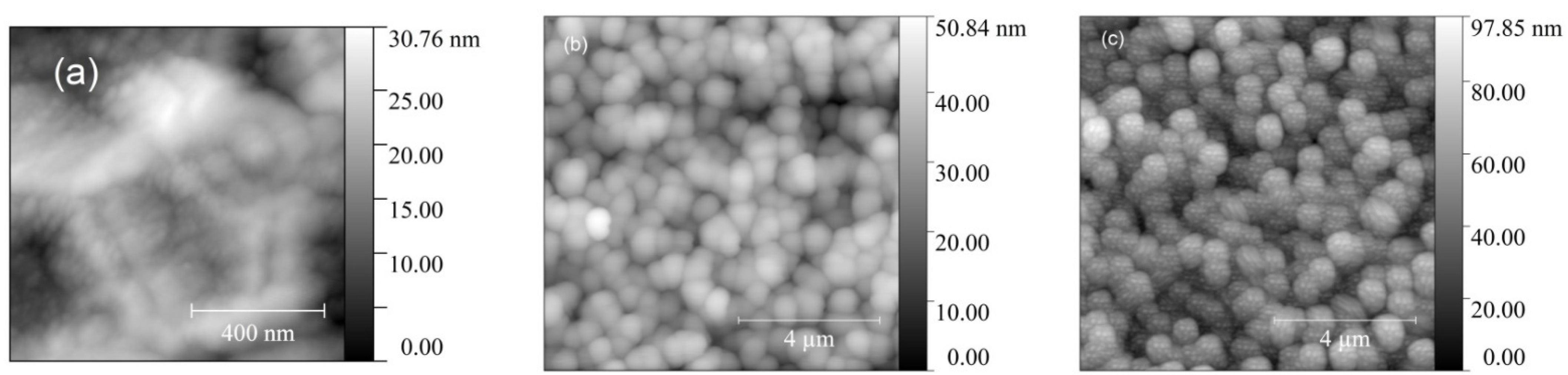
3.1. Structural Properties of TiO2 Films

The surface morphology of the as-deposited films consisted of grains, which, after annealing, formed large agglomerates (illustrated in Figure 1). The presence of a grain structure for films without annealing was caused by the low quality of the polycor substrate, which was considered appropriate to use for the manufacture of cheap sensor chips. The surface morphology parameters of the TiO2 thin films are compared in Table 2, where Da was the size of TiO2 agglomerates along the substrate plane and Dg was the TiO2 grain size along the substrate plane. An increase in d and Tann led to an increase in Da and Dg.
The XRD spectra of the as-prepared films, exhibited in Figure 2, demonstrated many low-intensity peaks that could be associated with different crystallographic planes of the corundum Al2O3 phase. The as-deposited films were amorphous and the XRD spectra of these films corresponded to polycrystalline sapphire substrate. After annealing, the positions of the Al2O3 peaks persisted, but the intensity of these peaks decreased. Peaks at 2θ = 39.7° and 2θ = 46.17° on the XRD spectra appeared after annealing. The second peak was associated with the (202) crystallographic plane of the Al2O3 [41]. The high-intensity peak at 2θ = 39.7° could be associated with the (200) crystallographic plane of the rutile TiO2 phase. The position of this peak did not depend on Tann. There was a slight shift in the positions of the peaks to the right, probably due to the presence of elastic deformations in the films after high-temperature annealing [42]. The XRD spectra of IBSD TiO2 thin films differed sharply from the spectra of TiO2 films and nanosized structures obtained by other methods [14,43,44,45,46]. The intense peak at 2θ = 38.65°, associated with the (200) crystallographic plane of the TiO2 rutile phase, was observed for MS deposited TiO2 thin films annealed at Tann = 900 °C [47]. The authors were unable to find data on the study of the XRD spectra of the IBSD deposited TiO2 thin films.
Direct optical transitions take place for TiO2 films, regardless of Tann, that is characteristic for the rutile phase [48,49]. An increase in Tann from 800 °C to 1000 °C led to a decrease in the energy of band gap Eg from 3.5 eV to 3.2 eV. The value Eg = 3.2 eV is typical for the rutile TiO2 phase [48,49]. The higher value of Eg at Tann = 800 °C could be explained by the existence of a small fraction of the anatase crystalline phase with a larger Eg in the TiO2 film’s structure.
Thus, it could be concluded that the annealed films composed of the rutile phase of TiO2. TiO2 films annealed at Tann = 800 °C might contain a small amount of the anatase modification. Increasing Tann up to 1000 °C led to the final transition of the TiO2 films into the high-temperature rutile phase.

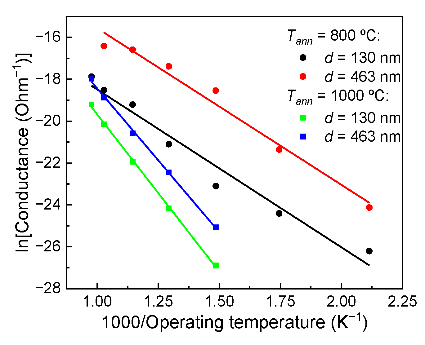
3.2. Electrically Conductive Properties of TiO2 Thin Films in Dry Pure Air

The I–V characteristics of TiO2 thin films with Pt contacts were linear in the ranges of U = 0–20 V, Toper = 200–750 °C and Toper = 400–750 °C after annealing at Tann = 800 °C and 1000 °C, respectively. For TiO2 films annealed at Tann = 800 °C the differential conductance Gd increased exponentially with Toper from 200 °C to 750 °C without any features characteristic of MOS thin films [50]. A decrease in the film thickness from 463 nm to 130 nm led to an increase in Gd by 1–2 orders of magnitude. An increase in Tann up to 1000 °C led to a decrease in Gd by 40 times at d = 130 nm and by 700 times at d = 463 nm. The activation energies of conduction ΔEd did not depend on d (Figure 3), at Tann = 800 °C ΔEd = 1.29 ± 0.08 eV and at Tann = 1000 °C ΔEd = 2.36 ± 0.05 eV.
The ΔEd of films annealed at Tann = 800 °C was close to the values for bulk samples obtained by ceramic technology with annealing at 800 °C [51]. The activation energy of films annealed at Tann = 1000 °C coincided with the value of ΔEd for single-crystal bulk samples obtained by the Verneuil melt method [52]. Such values of ΔEd are typical for high-temperature treatments, or grown methods, and are caused by the presence of oxygen vacancies in TiO2.

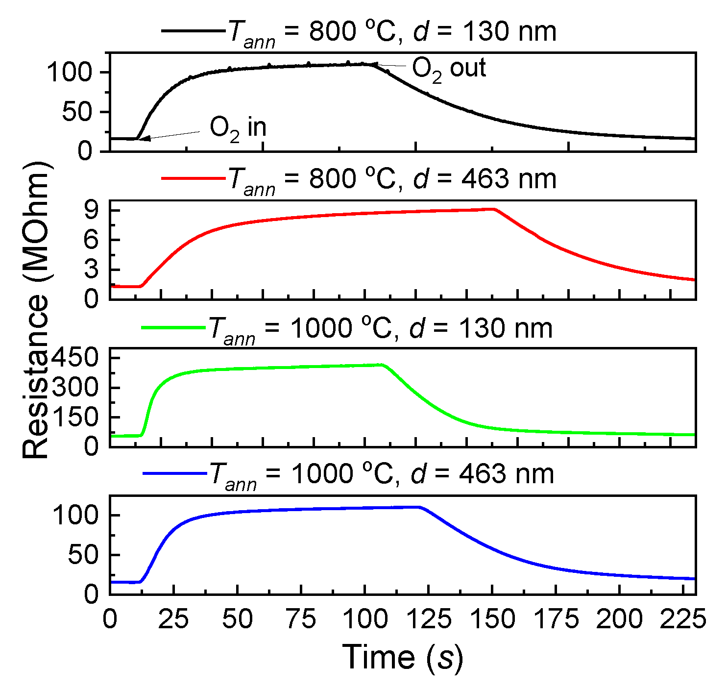
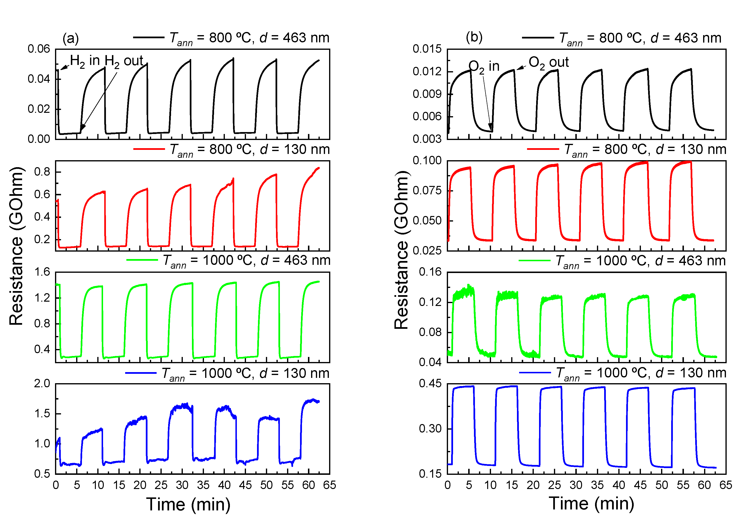
3.3. The Effect of Oxygen on the Electrically Conductive Properties of TiO2 Thin Films

TiO2 films are of interest for the development of high operating temperature O2 sensors for extreme environments [53,54,55], due to their high chemical and thermal stability. The effect of O2 led to a reversible increase in the resistance of TiO2 thin films placed in an atmosphere of dry N2 (Figure 4). The rise of the resistance of the film under exposure to O2, and the drop of resistance after this exposure, were approximated by the following functions, respectively:
R(t) = ROstAexp[−t/τ1],
R(t) = RNst + Bexp[−t/τ2],
where R is the resistance of a TiO2 thin film, t is time and ROst and RNst are the stationary values of the film resistance in the N2 + O2 mixture and in N2, respectively. A and B are constants; τ1 and τ2 are time constants. The operation speed of gas sensors is determined by response tres and recovery trec times. These values are given by the relaxation times of adsorption τA and desorption τD of gas molecules on the solid surface, τA & τD ~ exp[(ED–EA)/(2kT)], where ED and EA are the activation energies of desorption and adsorption processes of gas molecules on the semiconductor surface, k is the Boltzmann constant, and T is the absolute temperature of the semiconductor. The values, τA, τD, and, hence, tres, trec sharply decrease with Toper. The values τ1 and τ2 are related to τA and τD, respectively. From Equations (1) and (2), the exponents at t ≥ 2.3τ1 and t ≥ 2.3τ2 can be neglected. The resistance of the TiO2 thin film achieved ROst and RNst at t ≥ 2.3τ1 and t ≥ 2.3τ2. Thus, tres = 2.3τ1 and trec = 2.3τ2. Estimates of tres and trec for TiO2 thin films at Toper = 750 °C are presented in Table 3.
Increasing Tann at a fixed value of d and decreasing d at a fixed value of Tann led to a decrease in tres. Changing the film thickness at Tann = 800 °C did not affect trec, but, at Tann = 1000 °C, a decrease in the film’s thickness led to a decrease in trec by about 2 times. At d = 130 nm, an increase in Tann led to a significant decrease in trec by 1.8 times, and at d = 463 nm, there was a slight increase in trec. The increase in tres and trec with increasing d and fixed Tann are explained by the formation of a more developed surface. It slows down the diffusion of oxygen molecules and atoms, on the one hand, and of oxygen vacancies, on the other hand [56]. The decrease in tres with an increase in Tann and a fixed thickness was caused by an increase in the size of grains and agglomerates, which led to the opposite effect. It is worth noting that tres and trec contained the time required to establish the stationary state of the atmosphere in the measuring chamber, which, according to our estimates, could reach 6 s.
The following ratio, SO, was chosen as the film response to O2:
SO = ROst/RNst.
Films annealed at Tann = 800 °C showed sensitivity to O2 in the range of Toper = 300–750 °C (shown in Figure 5). For these films the maximum response was observed at Toper = 750 °C. At Toper = 700–750 °C films with d = 130 nm were characterized by the highest responses to O2. In the range of Toper = 300–600 °C TiO2 thin films with a thickness of 463 nm and annealed at Tann = 800 °C demonstrated a slightly higher response to O2.
For TiO2 thin films annealed at Tann = 1000 °C the response to O2 was measured in the range of Toper = 500–750 °C. At Toper = 300–500 °C and these films were not sensitive to O2. An increase in Tann led to a decrease in the response to O2 at fixed values of d, due to the effect of changes in the surface microrelief. The films were not sensitive to O2 at Toper = 300–500 °C for the same reason. A decrease in the response at fixed Toper with d was observed, due to an increase in the contribution of bulk conductivity. The maximum responses to O2 for these films within Toper range of 500–750 °C took place at Toper = 750 °C. We believe that the response for these films would increase with a further increase in Toper [1,2,3,8,9,10]. Measurements at Toper >750 °C were limited by the capabilities of measuring equipment.
The dependences of the TiO2 thin film responses to the O2 concentration at Toper = 750 °C (displayed in Figure 6) were approximated by the power function SO ~ nO2l, where nO2 is the O2 concentration and l is the power index. A change in the film thickness at a fixed value of Tann had little effect on the value of l (Table 4). An increase in Tann led to a decrease in l by ~0.025.

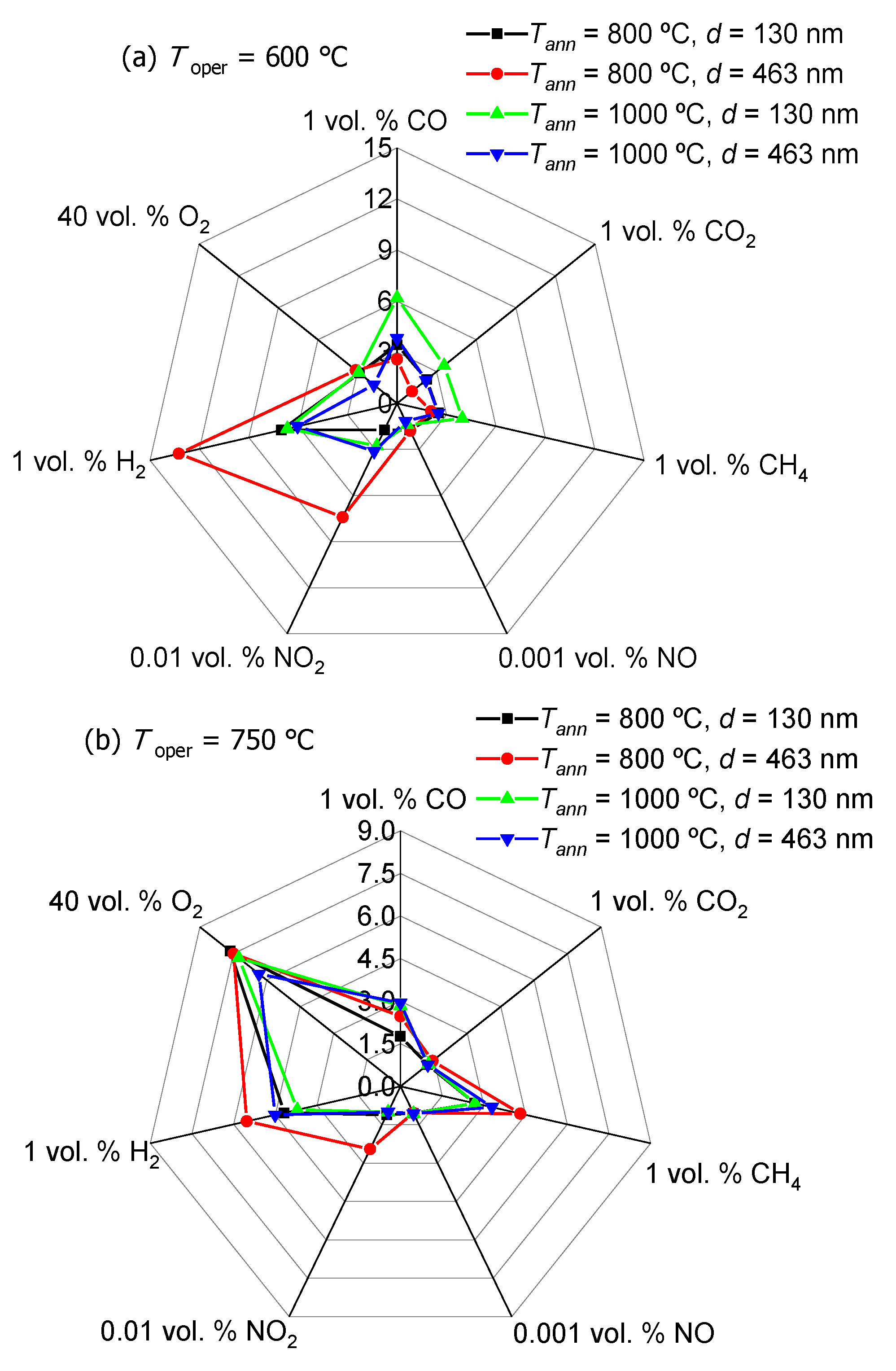
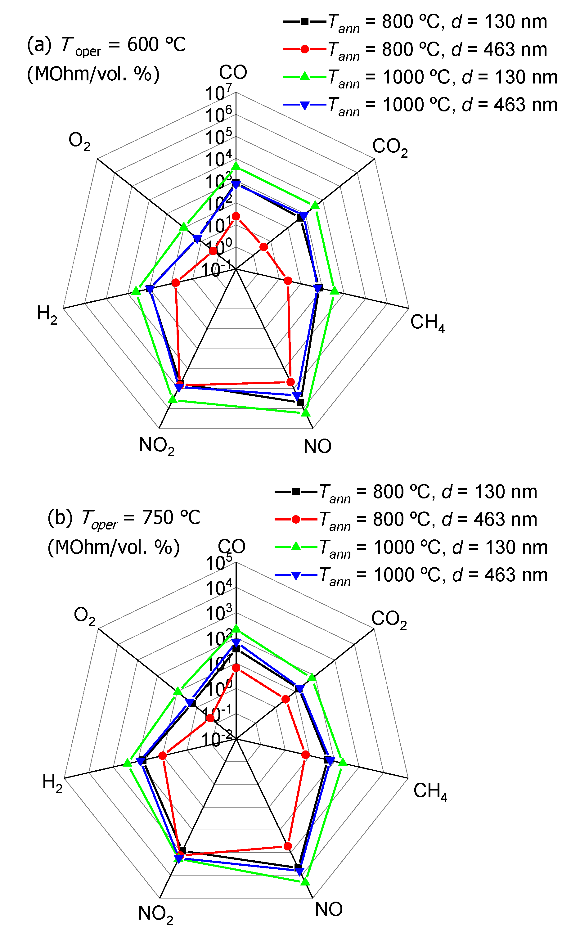
3.4. Sensitivity of TiO2 Thin Films to Reducing and Oxidizing Gases

At Toper = 600 °C and 750 °C the responses of TiO2 films to fixed concentrations of reducing and oxidizing gases were measured (Figure 7). The resistance of the films decreased when exposed to reducing gases: CO, CH4, and H2. Under exposure to oxidizing gases, CO2, NO and NO2, the resistance of the films reversibly increased. The responses to reducing gases were determined by the following formula:
S = Rairst/Rgst,
where Rairst and Rgst are stationary values of the TiO2 film resistance in dry pure air and in a mixture of dry pure air + target gas, respectively. The responses to oxidizing gases were determined by the inverse relation of (4).
TiO2 films at d = 463 nm and Tann = 800 °C demonstrated relatively high responses to 1 vol. % H2 and 0.01 vol. % NO2. TiO2 films at d = 130 nm and Tann = 1000 °C demonstrated relatively high responses to 1 vol. % CO, CO2 and CH4. At Toper = 600 °C responses to 40 vol. % O2 were lower than the responses to 1 vol. % H2, regardless of the film thickness and Tann, as well as being lower than the responses of TiO2 films at d = 130 nm and Tann = 1000 °C to 1 vol. % CO, CO2 and CH4. Responses of TiO2 films to fixed concentrations of other gases, in comparison with the response to 40 vol. % O2 at different d and Tann, were comparable or lower. Increasing the operating temperature of TiO2 thin films up to 750 °C, regardless of d and Tann, led to a decrease in responses to all gases, except for O2 and CH4. Responses to O2 and CH4 increased with T.
A more significant Increase in the response to O2, as well as a decrease in responses to other gases, should be expected with a further increase in Toper. It is believed that at Toper > 750 °C the sensitivity to gases is realized due to the interaction with oxygen vacancies [53,54,55]. In this operating temperature range the sensors should be selectively sensitive to O2. However, chemisorption of gas molecules on the semiconductor surface and their interaction with semiconductor defects can occur at Toper >750 °C. It often leads to the manifestation of high operating temperature sensitivity to reducing gases. Due to safety requirements and technical limitations the comparison of responses to the same concentration of different gases was not experimentally studied. For this reason, the sensitivity of TiO2 thin films to oxygen βO and other gases β was compared, using the following ratios, respectively:
βO = (ROstRNst)/nO2,
β = (RairstRgst)/ng for reducing gases,
β = (RgstRairst)/ng for oxidizing gases.
It is worth noting that the estimates of values βO and β (Figure 8) did not take into account the possible saturation of the gas-sensitive characteristics of the films under exposure to used gas concentrations. The films were characterized by the highest sensitivity to nitrogen oxides and showed approximately the same sensitivity to CO, CO2, CH4 and H2 at Toper = 600 °C, regardless of d and Tann. The lowest sensitivity of TiO2 films was realized when exposed to O2. An increase in Toper up to 750 °C led to a decrease in βO and β, due to a decrease in the base resistance. In this case, the ratios between the sensitivities to different gases were preserved. TiO2 films at d = 130 nm and Tann = 1000 °C were characterized by the highest sensitivity to gases. TiO2 films at d = 463 nm and Tann = 800 °C demonstrated the lowest sensitivity to gases.
The repeatability of IBSD TiO2 thin film characteristics was investigated under cyclic exposure to H2 and O2 gases (see Figure 9). Obviously, an increase in the thickness of films at a fixed Tann value led to an improvement in the repeatability of resistance and response of samples when exposed to H2. The standard deviations of S at d = 463 nm were 5% and 2% at Tann = 800 °C and 1000 °C, respectively. Response to H2 for films at d = 130 nm and Tann = 800 °C increased with each cycle of gas exposure, due to an increase in Rairst. For these films S increased 1.4 times after 6 cycles of H2 exposure. Films at d = 130 nm and Tann = 1000 °C were not characterized by high repeatability of the resistance and S under exposure to H2. The IBSD TiO2 thin films demonstrated high reproducibility of resistance and SO under cyclic exposure to O2. The standard deviations of SO when exposed to O2 were 1–2%. The reason for the instability of the IBSD fabricated TiO2 thin film characteristics at d = 130 nm might be the process of Ti reduction by hydrogen. This process was considered in detail for MS deposited SnO2 thin films at d = 100 nm [57]. The density of adsorption centers on the TiO2 film surface increases at Ti reduction by hydrogen. Oxygen is primarily chemisorbed onto these newly formed adsorption centers, which leads to an increase in Rairst and S. It is worth mentioning that this process became significant with a decrease in the film thickness, as the contribution of surface electrically conductance increased. The contribution of this process became insignificant with increasing d.
Thus, the IBSD TiO2 thin films demonstrated high sensitivity to H2, NO2 and exhibited potential for the development of O2 sensors operating at high temperatures. For this reason, a comparison of sensitivity to O2, H2 and NO2 for thin films obtained by different CVD and PVD methods is presented in Table 5, where CVD represents chemical vapor deposition. In Table 5, RFMS is radio-frequency magnetron sputtering, DCMS is direct-current magnetron sputtering, MOCVD is metalorganic chemical vapor deposition, EBE + oxidation is electron beam evaporation with following oxidation and ALD is atomic laser deposition.
The IBSD deposited TiO2 thin films were characterized by high response to O2 at high operating temperatures. In refs. [58,59] the sensitivity to O2 of much thinner TiO2 films were studied. UV irradiation of films was employed to increase the response at RT [59]. At the same time, tres was 360 s, which gave rise to significantly larger tres and trec for the IBSD TiO2 thin films (see Table 3).
The response to H2 of IBSD deposited TiO2 thin films was not high in comparison with other samples. The advantage of IBSD deposited TiO2 thin films was relatively high sensitivity at high operating temperatures, which is of interest for high operating temperature sensor applications. The high responses for DCMS and RFMS deposited films are due to the formation of Pt, Pd and PdO catalytic layers, as well as a fine-grained structure with Dg = 15 nm [60,61,64]. In most papers, tres and trec reached several min and even tens of min [47,62,64]. The repeatability of the TiO2 thin film characteristics when exposed to H2 was not practically considered. For IBSD deposited TiO2 thin films annealed at Tann = 1000 °C with d = 130 nm the lowest tres and trec were 23.4 s and 108.6 s, respectively.
IBSD deposited TiO2 thin films demonstrated the highest response to NO2. In references [65,66], TiO2 thin films showed sensitivity to gas at RT. However, the S was low, tres and trec were hundreds of s. In ref [66] the authors analyzed the effect of NO2 on frequency properties of TiO2 thin films. The frequency response was low.
It can be concluded that IBSD deposited TiO2 thin films are of interest for high operating temperature sensor applications. At the same time, in most of the research TiO2 thin films were modified with additives or irradiated with UV. The characteristics of such films and IBSD deposited TiO2 thin films are comparable in most cases. The capabilities of IBSD for the modification of TiO2 thin films [33,37] may allow the achieving of superior performance for sensors in the future.

3.5. Sensory Effect

Estimates for TiO2 thin films with a rutile structure showed that in the range of Toper = 300–750 °C, the ratio LD > Dg/2 took place, where LD is the Debye length. The possible inclusion of the anatase phase in TiO2 films annealed at Tann = 800 °C did not significantly affect the ratio between LD and Dg/2. Thus, the transport of charge carriers in TiO2 films was not affected by the presence of a potential barrier at the boundaries of small grains and large agglomerates that formed after annealing of the films. This is typical for IBSD deposited MOS films, as seen in Ref. [39].
The power index for films at Toper = 750 °C l = 0.20–0.23 (Table 4). The values of l at other identical conditions were determined by the film surface microrelief [67,68], which changed with varying annealing conditions. It was shown in ref [53] that l = ¼, 1/5 and 1/6 occurred at Toper > 800 °C and were characteristic for the interaction of oxygen molecules with TiO2 bulk defects, namely, oxygen vacancies and interstitial Ti atoms. A significant contribution to the gas sensitivity of TiO2 films, concerning the interaction of gas molecules, oxygen vacancies and other bulk defects at Toper ≤ 750 °C, could be neglected due to diffusion limitations [53,54,55]. The conductivity of the film changes as a result of chemisorption of gas molecules on the semiconductor surface. Oxygen molecules are chemisorbed on the film surface in an air atmosphere. Oxygen captures electrons from the conduction band of the semiconductor and forms a layer depleted in charge carriers on the film pre-surface region. Oxygen is chemisorbed on the semiconductor surface in the molecular O2(c) and atomic O(c), O2(c) forms [69]. The molecular form of chemisorbed oxygen dominated at Toper < 150 °C. With a further increase in T, dissociative adsorption of oxygen molecules took place and the predominant forms of chemisorbed oxygen were O(c) and O2(c). The obtained values of l ~0.25 indicated the predominance of O2(c) on the surface of TiO2 thin films. It is worth noting that the O(c) form was the most reactive. A negative charge on the surface of the n-type film led to the upward bending of energy bands eVs, where vs. is the surface potential, and e is the electron charge. In the value eVs~Ni2, Ni is the surface density of chemisorbed oxygen ions. The mechanism of the sensory effect described in ref [39] could be used for the IBSD TiO2 thin films. The total conductance of the TiO2 film was Gt = Gb + Gs, where Gb is the bulk conductance; Gs is the surface conductance. The value of Gs depends on the chemisorption of gas molecules on the semiconductor surface.
The expression describing the relationship between Gt and vs. for an n-type semiconductor at vs. > 0 has the following form ref [39]:
Gt = Gb × [1 − (LD/d) × [eVs/(kT)]]
It can be noted from expression (6) that an increase in the oxygen concentration in the chamber with TiO2 films led to a decrease in total conductance. Expression (6) took place at LD/d << 1 and a small band bending eVs/(kT) << 1. According to our estimates these inequalities were valid for our experimental conditions.
Interactions of previously chemisorbed O(c) and molecules of reducing gases can be represented in the following forms:
H2 + O(c) → H2O + e;
CO + O(c) → CO2 + e,
CH4 + 4O(c) → CO2 + 2H2O + 4e.
As a result of these reactions Ni, and eVs decrease, and electrons return to the conduction band of semiconductors. The reaction products between reducing gases and O(c) are desorbed as neutral CO2 and H2O molecules. The following reactions can occur on the semiconductor surface when exposed to oxidizing gases CO2, NO2, and NO, [70,71]:
NO2 + Sa + e → NO2,
NO2 + O(c) → NO3,
NO + Sa + e → NO,
NO + O(c) → NO2,
CO2 + Sa + e → CO2.
Molecules of oxidizing gases can be chemisorbed onto the free adsorption center Sa without the interaction with Oc ions capturing electrons from the conduction band of the semiconductor. In mixtures of air + NO2 eVs~(NiA + NNO2)2, air + NO eVs~(NiA + NNO)2 and air + CO2 eVs~(NiA + NCO2)2, where NiA is the surface density of chemisorbed oxygen ions in the air atmosphere; NNO2, NNO and NCO2 are the surface densities of chemisorbed NO2, NO & CO2-ions, respectively. An additional negative charge on the surface of TiO2 films leads to a greater increase in eVs and, consequently, to a decrease in their Gt. Equations (7) and (8) are the simplest possible, and fundamentally explain the observed sensory effect. Many reasonable variants of other reactions between gas molecules and previously chemisorbed O ions on the surface of metal oxide semiconductors have been proposed.
The interaction of gas molecules with O2(c) is not considered in detail in the literature. The authors in [72,73,74] consider that the processes of interactions of gas molecules with O(c) and O2(c) are similar, but the corresponding reactions are not given. It can be assumed that there is a step-by-step interaction of gas molecules with O2(c). At high operating temperatures O2(c) ions are predominant and a dissociative adsorption of gas molecules occurs on the semiconductor surface. In the example of H2, a similar process can be represented as follows:
H2 → 2H,
H + O2(c) → OH(c) + e;
OH(c) → OH + e.
After the dissociation of the molecule, the atomic hydrogen H interacts with the O2(c) ion, resulting in formation of a hydroxyl group OH(c) on the semiconductor surface with a localized electron, and an electron enters the TiO2 conduction band. The OH(c) groups neutralize and desorb on the semiconductor surface [75].

4. Conclusions

The structural, electrically conductive, and gas-sensitive properties of TiO2 films, with thicknesses of 130 nm and 463 nm, synthesized by the IBSD method, and subjected to high-temperature annealing in air were investigated. The IBSD TiO2 films annealed at 800 °C and 1000 °C belong to the rutile phase of TiO2. The electrically conductive properties of TiO2 thin films in dry pure air are similar to those of bulk samples obtained by melt and high-temperature methods. The effect of H2, CO, CO2, NO2, NO, CH4 and O2 on the electrically conductive properties of TiO2 thin films in the operating temperature range of 200–750 °C was studied. The prospects of TiO2 films deposited by IBSD for the development of high temperature operating O2 sensors were demonstrated. The operating temperature of the maximum response to O2 corresponded to 750 °C. TiO2 films with a thickness of 130 nm and annealed at 800 °C manifested the highest response to O2, which was 7.5 arb. un. when exposed to 40 vol. %. An increase in the annealing temperature up to 1000 °C at the same film thickness made it possible to reduce the response and recovery times by 2 times, due to changes appearing in the microstructure of the film surface. The films exhibited high responses to H2 and NO2 at an operating temperature of 600 °C and the largest sensitivity to nitrogen-containing oxides. An appropriate mechanism of the sensory effect in IBSD TiO2 thin films was proposed. The great significance of various atomic forms of chemisorbed oxygen on the semiconductor surface was revealed.

Author Contributions

Conceptualization, A.V.A.; methodology, B.O.K., V.V.K., V.A.N., M.M.Z., N.N.Y. (Nikolay N. Yudin) and A.V.C.; software, V.V.K.; validation, A.V.A. and N.N.Y. (Nikita N. Yakovlev); formal analysis, A.V.A., N.N.Y. (Nikita N. Yakovlev), V.V.K. and V.A.N.; investigation, N.N.Y. (Nikita N. Yakovlev), B.O.K., V.V.K., V.A.N., M.M.Z., N.N.Y. (Nikolay N. Yudin), S.N.P., N.N.E., A.V.C. and M.P.S.; resources, M.M.Z., N.N.E. and A.S.O.; data curation, A.V.A. and N.N.Y. (Nikita N. Yakovlev); writing—original draft preparation, H.B.; writing—review and editing, A.V.A.; visualization, N.N.Y. (Nikita N. Yakovlev); supervision, A.V.A.; project administration, A.V.A.; funding acquisition, A.V.A. All authors have read and agreed to the published version of the manuscript.

Funding

The research was carried out with the support of a grant under the Decree of the Government of the Russian Federation No. 220 of 9 April 2010 (Agreement No. 075-15-2022-1132 of 1 July 2022) and Ministry of Science and Higher Education of the Russian Federation, project No. FSWM-2020-0038. Studies of the deposition of TiO2 films by the IBS were supported by a grant from the Russian Science Foundation No. 22-22-20103 (https://rscf.ru/project/22-22-20103/ (accessed on 1 September 2022)) and funds of the Tomsk Region Administration.

Institutional Review Board Statement

Not applicable.

Informed Consent Statement

Not applicable.

Data Availability Statement

All data that support the findings of this study are included within the article.

Conflicts of Interest

The authors declare no conflict of interest.

References

  1. Wang, Y.; Wu, T.; Zhou, Y.; Meng, C.; Zhu, W.; Liu, L. TiO2-based nanoheterostructures for promoting gas sensitivity performance: Designs, developments, and prospects. Sensors 2017, 17, 1971. [Google Scholar] [CrossRef] [PubMed]
  2. Tian, X.; Cui, X.; Lai, T.; Ren, J.; Yang, Z.; Xiao, M.; Wang, B.; Xiao, X.; Wang, Y. Gas sensors based on TiO2 nanostructured materials for the detection of hazardous gases: A review. Nano Mater. Sci. 2021, 3, 390–403. [Google Scholar] [CrossRef]
  3. Rzaij, J.; Abass, A. Review on: TiO2 thin film as a metal oxide gas sensor. J. Chem. Rev. 2020, 2, 114–121. [Google Scholar] [CrossRef] [Green Version]
  4. Larsson, H.; Yakimova, R.; Zolnai, Z.; Ivanov, I.; Monemar, B.; Gogova, D. Fast growth of high quality GaN. Phys. Status Solidi a 2003, 20, 13–17. [Google Scholar] [CrossRef]
  5. Almaev, A.; Nikolaev, V.; Butenko, P.; Stepanov, S.; Pechnikov, A.; Yakovlev, N.; Sinyugin, I.; Shapenkov, S.; Scheglov, M. Gas sensors based on pseudohexagonal phase of gallium oxide. Phys. Status Solidi b 2021, 259, 2100306. [Google Scholar] [CrossRef]
  6. Kachel, K.; Korytov, M.; Gogova, D.; Galazka, Z.; Albrecht, M.; Zwierz, R.; Siche, D.; Golka, S.; Kwasniewski, A.; Schmidbauer, M.; et al. A new approach to free-standing GaN using β-Ga2O3 as a substrate. CrystEngComm 2012, 14, 8536–8540. [Google Scholar] [CrossRef]
  7. Almaev, A.V.; Yakovlev, N.N.; Chernikov, E.V.; Tolbanov, O.P. Selective sensors of nitrogen dioxide based on thin tungsten oxide films under optical irradiation. Tech. Phys. Lett. 2019, 45, 1016–1019. [Google Scholar] [CrossRef]
  8. Ramanavicius, S.; Tereshchenko, A.; Karpicz, R.; Ratautaite, V.; Bubniene, U.; Maneikis, A.; Jagminas, A.; Ramanavicius, A. TiO2-x/TiO2-structure based ‘self-heated’ sensor for the determination of some reducing gases. Sensors 2020, 20, 74. [Google Scholar] [CrossRef] [Green Version]
  9. Zakrzewska, K.; Radecka, M. TiO2-based nanomaterials for gas sensing—influence of anatase and rutile contributions. Nanoscale Res. Lett. 2017, 12, 89. [Google Scholar] [CrossRef] [Green Version]
  10. Li, Z.; Jun, Y.X.; Haidry, A.A.; Plecenik, T.; Juan, X.L.; Chao, S.L.; Fatima, Q. Resistive-type hydrogen gas sensor based on TiO2: A review. Int. J. Hydrogen Energy 2018, 43, 21114–21132. [Google Scholar] [CrossRef]
  11. Nunes, D.; Fortunato, E.; Martins, R. Flexible nanostructured TiO2-based gas and UV sensors: A review. Discov. Mater. 2022, 2, 2. [Google Scholar] [CrossRef]
  12. Li, T.; Rui, Y.; Zhang, X.; Shi, J.; Wang, X.; Wang, Y.; Yang, J.; Zhang, Q. Anatase TiO2 nanorod arrays as high-performance electron transport layers for perovskite solar cells. J. Alloys Compd. 2020, 849, 156629. [Google Scholar] [CrossRef]
  13. Illarionov, G.A.; Morozova, S.M.; Chrishtop, V.V.; Einarsrud, M.A.; Morozov, M.I. Memristive TiO2: Synthesis, technologies, and applications. Front. Chem. 2020, 8, 724. [Google Scholar] [CrossRef] [PubMed]
  14. Lin, J.; Heo, Y.U.; Nattestad, A.; Sun, Z.; Wang, L.; Kim, J.H.; Dou, Z.X. 3D hierarchical rutile TiO2 and metal-free organic sensitizer producing dye-sensitized solar cells 8.6 % conversion efficiency. Sci. Rep. 2014, 4, 5769. [Google Scholar] [CrossRef] [PubMed] [Green Version]
  15. He, X.; Wu, M.; Ao, Z.; Lai, B.; Zhou, Y.; An, T.; Wang, S. Metal–organic frameworks derived C/TiO2 for visible light photocatalysis: Simple synthesis and contribution of carbon species. J. Hazard. Mater. 2021, 403, 124048. [Google Scholar] [CrossRef]
  16. Ratan, S.; Kumar, C.; Kumar, A.; Kumar, D.J.; Kumar, A.M.; Kumar, R.U.; Pratap, A.S.; Jit, S. Room temperature high hydrogen gas response in Pd/TiO2/Si/Al capacitive sensor. Micro Nano Lett. 2020, 15, 632–635. [Google Scholar] [CrossRef]
  17. Dwivedi, D.; Dwivedi, R.; Srivastava, S.K. The effect of hydrogen-induced interface traps on a titanium dioxide-based palladium gate MOS capacitor (Pd-MOSC): A conductance study. Microelectron. J. 1998, 29, 445–450. [Google Scholar] [CrossRef]
  18. Mardare, D.; Cornei, N.; Mita, C.; Florea, D.; Stancu, A.; Tiron, V.; Manole, A.; Adomnitei, C. Low temperature TiO2 based gas sensors for CO2. Ceram. Int. 2016, 42, 7353–7359. [Google Scholar] [CrossRef]
  19. Rydosz, A.; Brudnik, A.; Staszek, K. Metal oxide thin films prepared by magnetron sputtering technology for volatile organic compound detection in the microwave frequency range. Materials 2019, 12, 877. [Google Scholar] [CrossRef] [Green Version]
  20. Moumen, A.; Kumarage, G.C.W.; Comini, E. P-type metal oxide semiconductor thin films: Synthesis and chemical sensor applications. Sensors 2022, 22, 1359. [Google Scholar] [CrossRef]
  21. Nafarizal, N. Precise control of metal oxide thin films deposition in magnetron sputtering plasmas for high performance sensing devices fabrication. Procedia Chem. 2016, 20, 93–97. [Google Scholar] [CrossRef]
  22. Chaluvadi, S.K.; Mondal, D.; Bigi, C.; Knez, D.; Rajak, P.; Ciancio, R.; Fujii, J.; Panaccione, G.; Vobornik, I.; Rossi, G.; et al. Pulsed laser deposition of oxide and metallic thin films by means of Nd:YAG laser source operating at its 1st harmonics: Recent approaches and advances. J. Phys. Mater. 2021, 4, 032001. [Google Scholar] [CrossRef]
  23. Filipescu, M.; Papavlu, A.P.; Dinescu, M. Functional metal oxide thin films grown by pulsed laser deposition. In Crystalline and Non-Crystalline Solids; Mandracci, P., Ed.; IntechOpen: London, UK, 2016. [Google Scholar] [CrossRef] [Green Version]
  24. Huotari, J.; Kekkonen, V.; Puustinen, J.; Liimatainen, J.; Lappalainen, J. Pulsed laser deposition for improved metal-oxide gas sensing layers. Procedia Eng. 2016, 168, 1066–1069. [Google Scholar] [CrossRef]
  25. Huotari, J.; Lappalainen, J.; Puustinen, J.; Baur, T.; Alepee, C.; Haapalainen, T.; Komulainen, S.; Pylvanainen, J.; Lloyd, A.S. Pulsed laser deposition of metal oxide nanoparticles, agglomerates, and nanotrees for chemical sensors. Procedia Eng. 2015, 120, 1158–1161. [Google Scholar] [CrossRef] [Green Version]
  26. Hamid, N.; Suhaimi, S.; Othman, M.Z.; Ismail, W.Z.W. A Review on thermal evaporation method to synthesis zinc oxide as photocatalytic material. Nano Hybrids Compos. 2021, 31, 55–63. [Google Scholar] [CrossRef]
  27. Mukherjee, S. Thin film deposition from dual ion beam sputtering system. CSI Trans. ICT 2019, 7, 99–104. [Google Scholar] [CrossRef]
  28. Bundesmann, C.; Neumann, H. Tutorial: The systematics of ion beam sputtering for deposition of thin films with tailored properties. J. Appl. Phys. 2018, 124, 231102. [Google Scholar] [CrossRef]
  29. Bundesmann, C.; Amelal, T. Secondary particle properties for the ion beam sputtering of TiO2 in a reactive oxygen atmosphere. Appl. Surf. Sci. 2019, 485, 391–401. [Google Scholar] [CrossRef]
  30. Bundesmann, C.; Lautenschläger, T.; Spemann, D.; Finzel, A.; Thelander, E.; Mensing, M.; Frost, F. Systematic investigation of the properties of TiO2 films grown by reactive ion beam sputter deposition. Appl. Surf. Sci. 2017, 421, 331–340. [Google Scholar] [CrossRef]
  31. Bundesmann, C.; Lautenschläger, T.; Spemann, D.; Thelander, E. Reactive Ar ion beam sputter deposition of TiO2 films: Influence of process parameters on film properties. Nucl. Instrum. Methods Phys. Res. Sect. B Beam Interact. Mater. At. 2017, 395, 17–23. [Google Scholar] [CrossRef]
  32. Amelal, T.; Pietzonka, L.; Rohkamm, E.; Bundesmann, C. Properties of secondary particles for the reactive ion beam sputtering of Ti and TiO2 using oxygen ions. J. Vac. Sci. Technol. A 2020, 38, 033403. [Google Scholar] [CrossRef]
  33. Jung, H.; Min, H.; Hwang, J.; Kim, J.; Choe, Y.; Lee, H.; Lee, W. Selective detection of sub-1-ppb level isoprene using Pd-coated In2O3 thin film integrated in portable gas chromatography. Appl. Surf. Sci. 2022, 586, 152827. [Google Scholar] [CrossRef]
  34. Kalanov, D.; Unutulmazsoy, Y.; Spemann, D.; Bauer, J.; Anders, A.; Bundesmann, C. Properties of gallium oxide thin films grown by ion beam sputter deposition at room temperature. J. Vac. Sci. Technol. A 2022, 40, 033409. [Google Scholar] [CrossRef]
  35. Choe, Y. New gas sensing mechanism for SnO2 thin-film gas sensors fabricated by using dual ion beam sputtering. Sens. Actuators B Chem. 2001, 77, 200–208. [Google Scholar] [CrossRef]
  36. Min, B.K.; Choi, S.D. C4H10 sensing characteristics of ion beam sputtered SnO2 sensors. Sens. Actuators B Chem. 2005, 108, 125–129. [Google Scholar] [CrossRef]
  37. Min, B.K.; Choi, S.D. SnO2 thin film gas sensor fabricated by ion beam deposition. Sens. Actuators B Chem. 2004, 98, 239–246. [Google Scholar] [CrossRef]
  38. Prasad, A.K.; Kubinski, D.J.; Gouma, P.I. Comparison of sol–gel and ion beam deposited MoO3 thin film gas sensors for selective ammonia detection. Sens. Actuators B Chem. 2003, 93, 25–30. [Google Scholar] [CrossRef]
  39. Simion, C.E.; Schipani, F.; Papadogianni, A.; Stanoiu, A.; Budde, M.; Oprea, A.; Weimar, U.; Bierwagen, O.; Barsan, N. Conductance model for single-crystalline/compact metal oxide gas-sensing layers in the nondegenerate limit: Example of epitaxial SnO2 (101). ACS Sens. 2019, 4, 2420–2428. [Google Scholar] [CrossRef]
  40. Liu, Y.; Parisi, J.; Sun, X.; Lei, Y. Solid-state gas sensors for high temperature applications—A review. J. Mater. Chem. A 2014, 2, 9919. [Google Scholar] [CrossRef]
  41. Golubović, A.; Nikolić, S.; Djurić, S.; Valčić, A. The growth of sapphire single crystals. J. Serb. Chem. Soc. 2001, 66, 411–418. [Google Scholar] [CrossRef]
  42. Almaev, A.V.; Kushnarev, B.O.; Chernikov, E.V.; Novikov, V.A.; Korusenko, P.M.; Nesov, S.N. Structural, electrical and gas-sensitive properties of Cr2O3 thin films. Superlattices Microstruct. 2021, 151, 106835. [Google Scholar] [CrossRef]
  43. Qing, H.; Lian, G. A simple route for the synthesis of rutile TiO2 nanorods. Chem. Lett. 2003, 32, 638–639. [Google Scholar] [CrossRef]
  44. Wang, D.; Choi, D.; Yang, Z.; Viswanathan, V.V.; Nie, Z.; Wang, C.; Song, Y.; Zhang, J.-G.; Liu, J. Synthesis and Li-ion insertion properties of highly crystalline mesoporous rutile TiO2. Chem. Mater. 2008, 20, 3435–3442. [Google Scholar] [CrossRef]
  45. Abazović, N.D.; Čomor, M.I.; Dramićanin, M.D.; Jovanović, D.J.; Ahrenkiel, S.P.; Nedeljković, J.M. Photoluminescence of anatase and rutile TiO2 particles. J. Phys. Chem. B 2006, 110, 25366–25370. [Google Scholar] [CrossRef] [PubMed]
  46. Miao, L.; Jin, P.; Kaneko, K.; Terai, A.; Nabatova-Gabain, N.; Tanemura, S. Preparation and characterization of polycrystalline anatase and rutile TiO2 thin films by rf magnetron sputtering. Appl. Surf. Sci. 2003, 212–213, 255–263. [Google Scholar] [CrossRef]
  47. Haidry, A.A.; Schlosser, P.; Durina, P.; Mikula, M.; Tomasek, M.; Plecenik, T.; Roch, T.; Pidik, A.; Stefecka, M.; Noskovic, J.; et al. Hydrogen gas sensors based on nanocrystalline TiO2 thin films. Cent. Eur. J. Phys. 2011, 9, 1351. [Google Scholar] [CrossRef]
  48. Nadzirah, S.; Hashim, U.; Kashif, M.; Shamsuddin, S.A. Stable electrical, morphological and optical properties of titanium dioxide nanoparticles affected by annealing temperature. Microsyst. Technol. 2017, 23, 1743–1750. [Google Scholar] [CrossRef]
  49. Soussi, A.; Ait Hssi, A.; Boujnah, M.; Boulkadat, L.; Abouabassi, K.; Asbayou, A.; Elfanaoui, A.; Markazi, R.; Ihlal, A.; Bouabid, K. Electronic and optical properties of TiO2 thin films: Combined experimental and theoretical study. J. Electron. Mater. 2021, 50, 4497–4510. [Google Scholar] [CrossRef]
  50. Korotcenkov, G.; Brinzari, V.; Golovanov, V.; Blinov, Y. Kinetics of gas response to reducing gases of SnO2 films, deposited by spray pyrolysis. Sens. Actuators B Chem. 2004, 98, 41–45. [Google Scholar] [CrossRef]
  51. Weibel, A.; Bouchet, R.; Knauth, P. Electrical properties and defect chemistry of anatase (TiO2). Solid State Ion. 2006, 177, 229–236. [Google Scholar] [CrossRef] [Green Version]
  52. Nowotny, M.K.; Bak, T.; Nowotny, J. Electrical properties and defect chemistry of TiO2 single crystal. I. Electrical conductivity. J. Phys. Chem. B 2006, 110, 16270–16282. [Google Scholar] [CrossRef] [PubMed]
  53. Gan, L.; Wu, C.; Tan, Y.; Chi, B.; Pu, J.; Jian, L. Oxygen sensing performance of Nb-doped TiO2 thin film with porous structure. J. Alloy. Compd. 2014, 585, 729–733. [Google Scholar] [CrossRef]
  54. Li, M.; Chen, Y. An investigation of response time of TiO2 thin-film oxygen sensors. Sens. Actuators B Chem. 1996, 32, 83–85. [Google Scholar] [CrossRef]
  55. Kirner, U.; Schierbaum, K.D.; Göpel, W.; Leibold, B.; Nicoloso, N.; Weppner, W.; Fischer, D.; Chu, W.F. Low and high temperature TiO2 oxygen sensors. Sens. Actuators B Chem. 1990, 1, 103–107. [Google Scholar] [CrossRef]
  56. Bartic, M.; Toyoda, Y.; Baban, C.; Ogita, M. Oxygen sensitivity in gallium oxide thin films and single crystals at high temperatures. Jpn. J. Appl. Phys. 2006, 45, 5186. [Google Scholar] [CrossRef]
  57. Maksimova, N.K.; Almaev, A.V.; Sevastyanov, E.Y.; Potekaev, A.I.; Chernikov, E.V.; Sergeychenko, N.V.; Korusenko, P.M.; Nesov, S.N. Effect of additives Ag and rare-earth elements Y and Sc on the properties of hydrogen sensors based on thin SnO2 films during long-term testing. Coatings 2019, 9, 423. [Google Scholar] [CrossRef] [Green Version]
  58. Lu, C.; Huang, Y.; Huang, J.; Chang, C.; Wu, S. A Macroporous TiO2 oxygen sensor fabricated using anodic aluminium oxide as an etching mask. Sensors 2010, 10, 670–683. [Google Scholar] [CrossRef]
  59. Wang, Y.; Lai, X.; Liu, B.; Chen, Y.; Lu, Y.; Wang, F.; Zhang, L. UV-induced desorption of oxygen at the TiO2 surface for highly sensitive room temperature O2 sensing. J. Alloy. Compd. 2019, 793, 583–589. [Google Scholar] [CrossRef]
  60. Haidry, A.A.; Xie, L.; Wang, Z.; Zavabeti, A.; Li, Z.; Plecenik, T.; Gregor, M.; Roch, T.; Plecenik, A. Remarkable improvement in hydrogen sensing characteristics with Pt/TiO2 interface control. ACS Sens. 2019, 4, 2997–3006. [Google Scholar] [CrossRef]
  61. Kumar, M.; Singh Bhati, V.; Kumar, M. Effect of Schottky barrier height on hydrogen gas sensitivity of metal/TiO2 nanoplates. Int. J. Hydrog. Energy 2017, 42, 22082–22089. [Google Scholar] [CrossRef]
  62. Arifin, P.; Mustajab, M.A.; Haryono, S.; Adhika, D.R.; Nugraha, A.A. MOCVD growth and characterization of TiO2 thin films for hydrogen gas sensor application. Mater. Res. Express 2019, 6, 076313. [Google Scholar] [CrossRef]
  63. Lu, C.; Chen, Z. High-temperature resistive hydrogen sensor based on thin nanoporous rutile TiO2 film on anodic aluminum oxide. Sens. Actuators B Chem. 2009, 140, 109–115. [Google Scholar] [CrossRef]
  64. Samransuksamer, B.; Jutarosaga, T.; Horprathum, M.; Wisitsoraat, A.; Eiamchai, P.; Limwichean, S.; Patthanasettakul, V.; Chananonnawathorn, C.; Chindaudom, P. Highly sensitive H2 sensors based on Pd- and PdO-decorated TiO2 thin films at low-temperature operation. Key Eng. Mater. 2016, 675–676, 277–280. [Google Scholar] [CrossRef]
  65. Xie, T.; Sullivan, N.; Steffens, K.; Wen, B.; Liu, G.; Debnath, R.; Davydov, A.; Gomez, R.; Motayed, A. UV-assisted room-temperature chemiresistive NO2 sensor based on TiO2 thin film. J. Alloy. Compd. 2015, 653, 255–259. [Google Scholar] [CrossRef] [PubMed] [Green Version]
  66. Boyadjiev, S.; Georgieva, V.; Vergov, L.; Baji, Z.; Gáber, F.; Szilágyi, I.M. Gas sensing properties of very thin TiO2 films prepared by atomic layer deposition (ALD). J. Phys. Conf. Ser. 2014, 559, 012013. [Google Scholar] [CrossRef]
  67. Rumyantseva, M.N.; Makeeva, E.A.; Gaskov, A.M. Influence of the microstructure of semiconductor sensor materials on oxygen chemisorption on their surface. Russ. J. Gen. Chem. 2008, 78, 2556–2565. [Google Scholar] [CrossRef]
  68. Almaev, A.V.; Chernikov, E.V.; Novikov, V.V.; Kushnarev, B.O.; Yakovlev, N.N.; Chuprakova, E.V.; Oleinik, V.L.; Lozinskaya, A.D.; Gogova, D.S. Impact of Cr2O3 additives on the gas-sensitive properties of β-Ga2O3 thin films to oxygen, hydrogen, carbon monoxide, and toluene vapors. J. Vac. Sci. Technol. A 2021, 39, 023405. [Google Scholar] [CrossRef]
  69. Saruhan, B.; Fomekong, L.R.; Nahirniak, S. Review: Influences of semiconductor metal oxide properties on gas sensing characteristics. Front. Sens. 2021, 2, 657931. [Google Scholar] [CrossRef]
  70. Badalyan, S.M.; Rumyantseva, M.N.; Smirnov, V.V.; Alikhanyan, A.S.; Gaskov, A.M. Effect of Au and NiO catalysts on the NO2 sensing properties of nanocrystalline SnO2. Inorg. Mater. 2010, 46, 232–236. [Google Scholar] [CrossRef]
  71. Gautam, Y.K.; Sharma, K.; Tyagi, S.; Ambedkar, A.K.; Chaudhary, M. Nanostructured metal oxide semiconductor-based sensors for greenhouse gas detection: Progress and challenges. R. Soc. Open Sci. 2021, 8, 201324. [Google Scholar] [CrossRef]
  72. Jiménez-Cadena, G.; Riu, J.; Rius, F.X. Gas sensors based on nanostructured materials. Analyst 2007, 132, 1083–1099. [Google Scholar] [CrossRef]
  73. Yamazoe, N.; Fuchigami, J.; Kishikawa, M.; Seiyama, T. Interactions of tin oxide surface with O2, H2O and H2. Surf. Sci. 1979, 86, 335–344. [Google Scholar] [CrossRef]
  74. Yamazoe, N.; Sakai, G.; Shimanoe, K. Oxide semiconductor gas sensors. Catal. Surv. Asia 2003, 7, 63–75. [Google Scholar] [CrossRef]
  75. Gaman, V.I.; Almaev, A.V. Dependences of characteristics of sensors based on tin dioxide on the hydrogen concentration and humidity of gas mixture. Russ. Phys. J. 2017, 60, 90–100. [Google Scholar] [CrossRef]
Figure 1. AFM images of TiO2 thin films surface at d = 463 nm and Tann = 0 (a), Tann = 800 ℃ (b); Tann = 1000 ℃ (c).
Coatings 12 01565 g001
Figure 2. XRD spectra of TiO2 films annealed at Tann = 800 °C and 1000 °C.
Coatings 12 01565 g002
Figure 3. Arrhenius curves for TiO2 films after annealing at Tann = 800 °C and 1000 °C.
Coatings 12 01565 g003
Figure 4. Time dependences of the TiO2 thin films resistances upon exposure to 40 vol. % O2 and Toper = 750 °C.
Coatings 12 01565 g004
Figure 5. Dependences of the response to 40 vol. % O2 on operating temperature.
Coatings 12 01565 g005
Figure 6. Dependences of the response on the O2 concentration at Toper = 750 °C.
Coatings 12 01565 g006
Figure 7. Responses to fixed concentrations of various gases at Toper = 600 ℃ (a) and Toper = 750 ℃ (b).
Coatings 12 01565 g007
Figure 8. Sensitivity of TiO2 thin films to various gases at Toper = 600 °C (a) and Toper = 750 °C (b).
Coatings 12 01565 g008
Figure 9. Time dependences of the TiO2 thin films resistances upon exposure to 1 vol. % H2 at Toper = 600 °C (a) and upon exposure to 40 vol. % O2 at Toper = 750 °C (b).
Coatings 12 01565 g009
Table 1. Gas sensitive characteristics of IBSD metal oxide semiconductors (MOS) thin films.
MOSd (nm)Gasng (vol. %)TMAX (°C)SRef.
In2O340Isoprene25 × 10−44321.02[33]
Au/In2O33642.82
Pt/In2O32552.51
Pd/In2O31966.31
SnO210H20.135020[35]
2025
5060
10070
20030
50020
SnO250C4H100.54004[36]
Pt/SnO24.5
SnO2:Ca2.5
Pt/SnO2:Ca2.3
SnO250CH40.54001.75[37]
SnO2:Ca1.4
MoO3-NH30.014504[38]
Table 2. Surface microrelief parameters of TiO2 thin films.
d (nm)Tann (℃)Da (nm)Dg (nm)
1300-10–30
800320–550100
1000500–700125
4630-10–30
800350–600100–110
1000600–800150
Table 3. Response and recovery times of TiO2 thin films upon exposure to 40 vol. % O2 and Toper = 750 °C.
Tann (℃)d (nm)tres (s)trec (s)
80013035.085.3
46354.785.1
100013012.647.8
46323.992.6
Table 4. Power indexes l for TiO2 thin films at Toper = 750 °C.
Tann (°C)d (nm)l
8001300.227 ± 0.004
4630.235 ± 0.006
10001300.195 ± 0.003
4630.212 ± 0.002
Table 5. Comparison of sensitivity to O2, H2 and NO2 for thin films deposited by different CVD and PVD methods.
Methodsd (nm)ng (vol. %)Toper (°C)SRef.
O2
RFMS500.65001.14[58]
DCMS6010RT76[59]
IBSD130407507.64This work
H2
DCMS501450~104[47]
DCMS1601120107[60]
RFMS~30011751.8[61]
MOCVD7111001.3[62]
EBE + oxidation250.0550091[63]
DCMS40031501.1 × 104[64]
IBSD463160013.25This work
NO2
RFMS100.05RT1.021[65]
ALD80.1RT7.5 × 10−7 *[66]
IBSD4630.016007.41This work
* The response was determined from the frequency properties.
Publisher’s Note: MDPI stays neutral with regard to jurisdictional claims in published maps and institutional affiliations.

