Ultrafast Patterning Vertically Aligned Carbon Nanotube Forest on Al Foil and Si Substrate Using Chemical Vapor Deposition (CVD)

Abstract
:1. Introduction
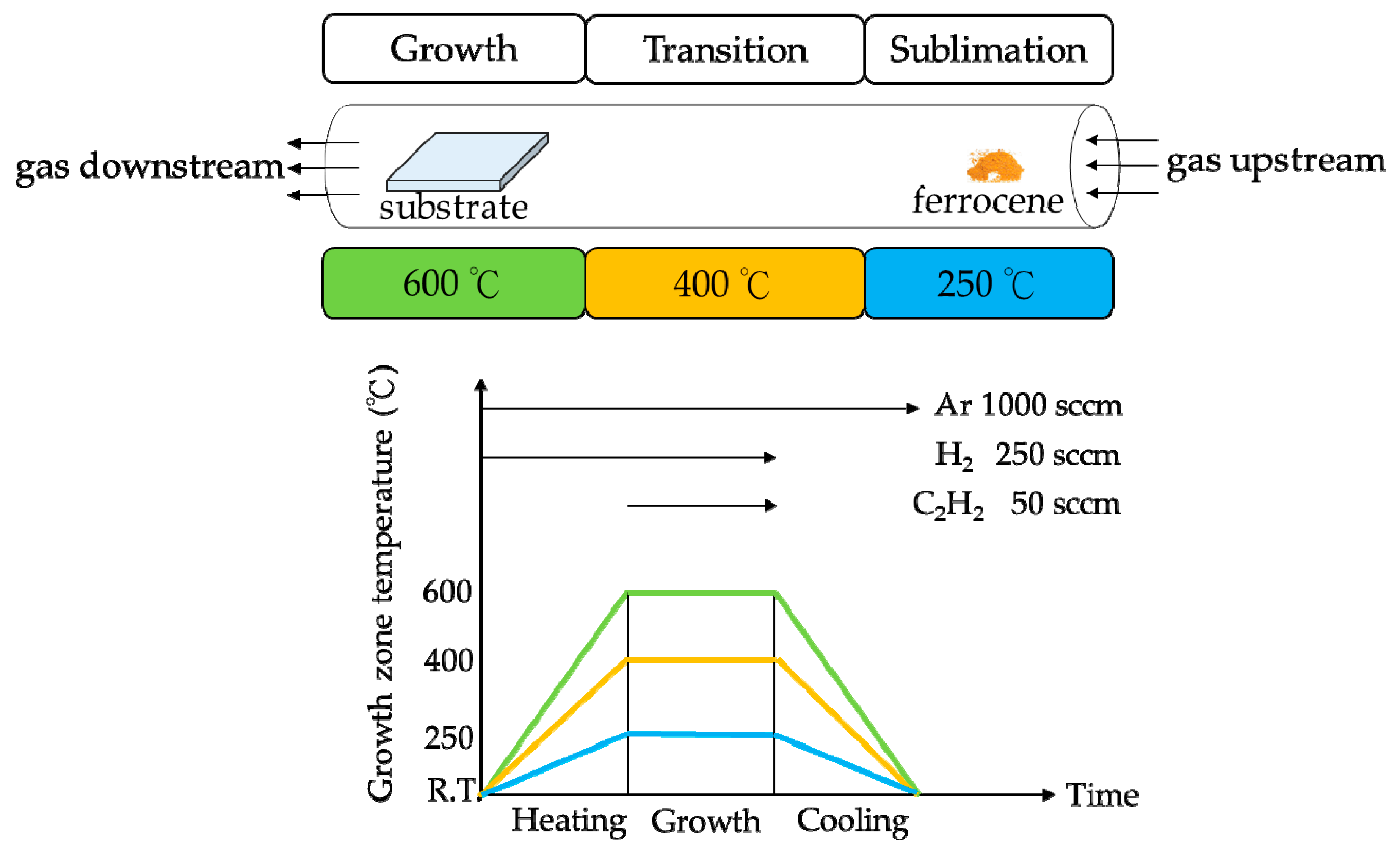
2. Experiments
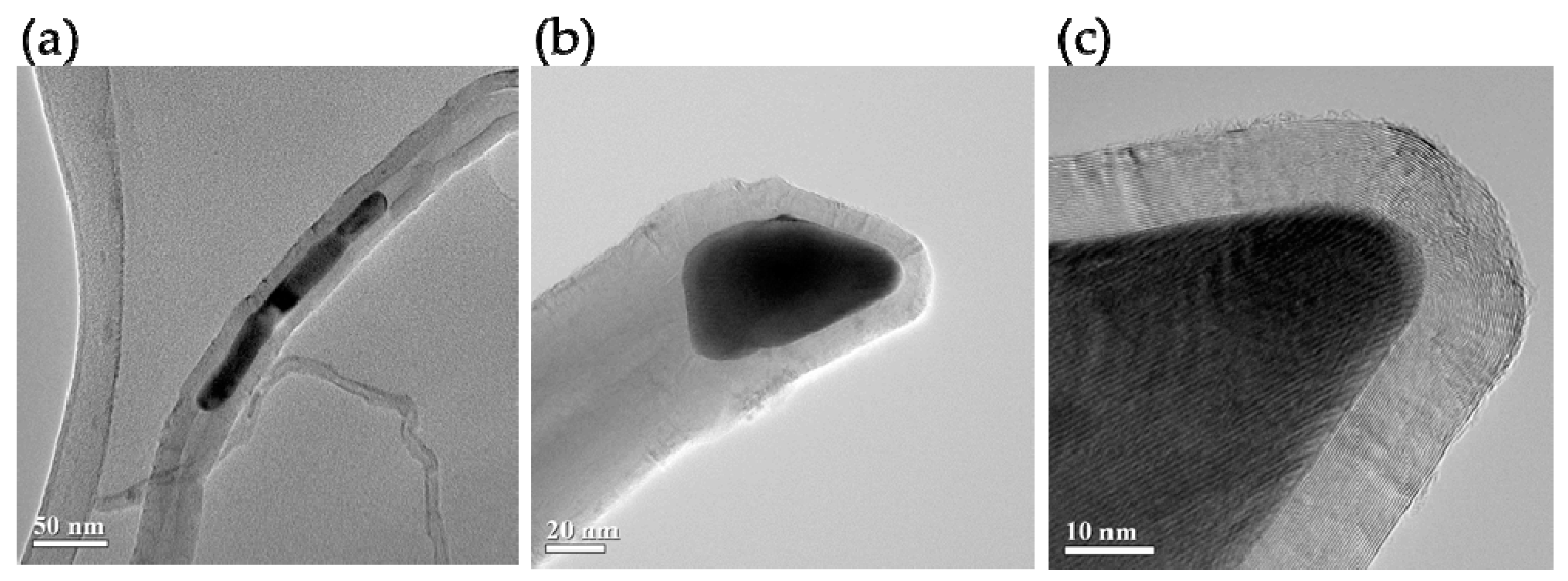
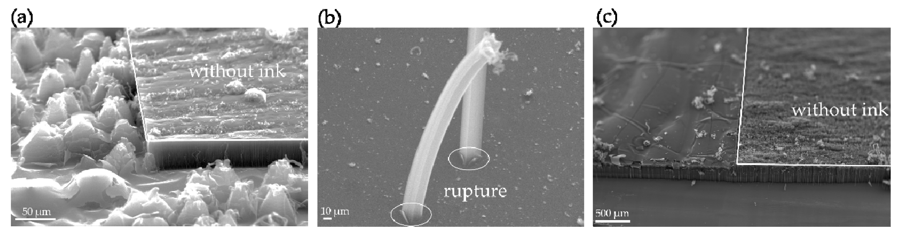
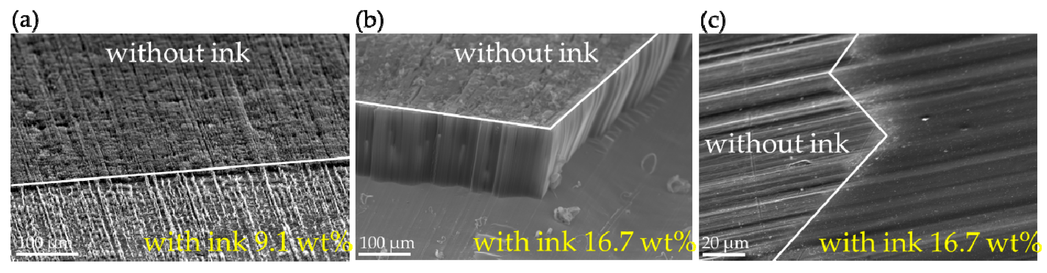
3. Results and Discussions
4. Conclusions
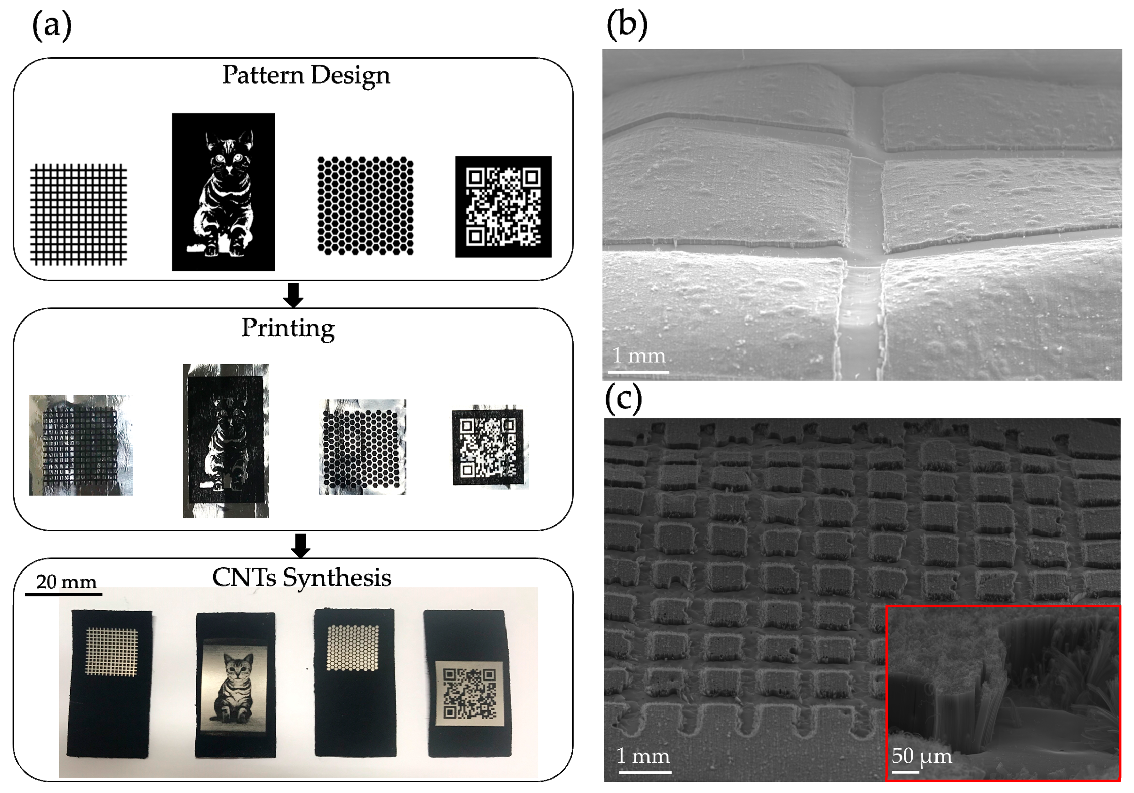
- The initial ink printing method turned up several issues, including how to smoothly feed aluminum foil into the printer, how to avoid ink splattering, and how to enhance pattern resolution. If equipment was developed that addressed these issues, the ink printing method would have a much broader application.
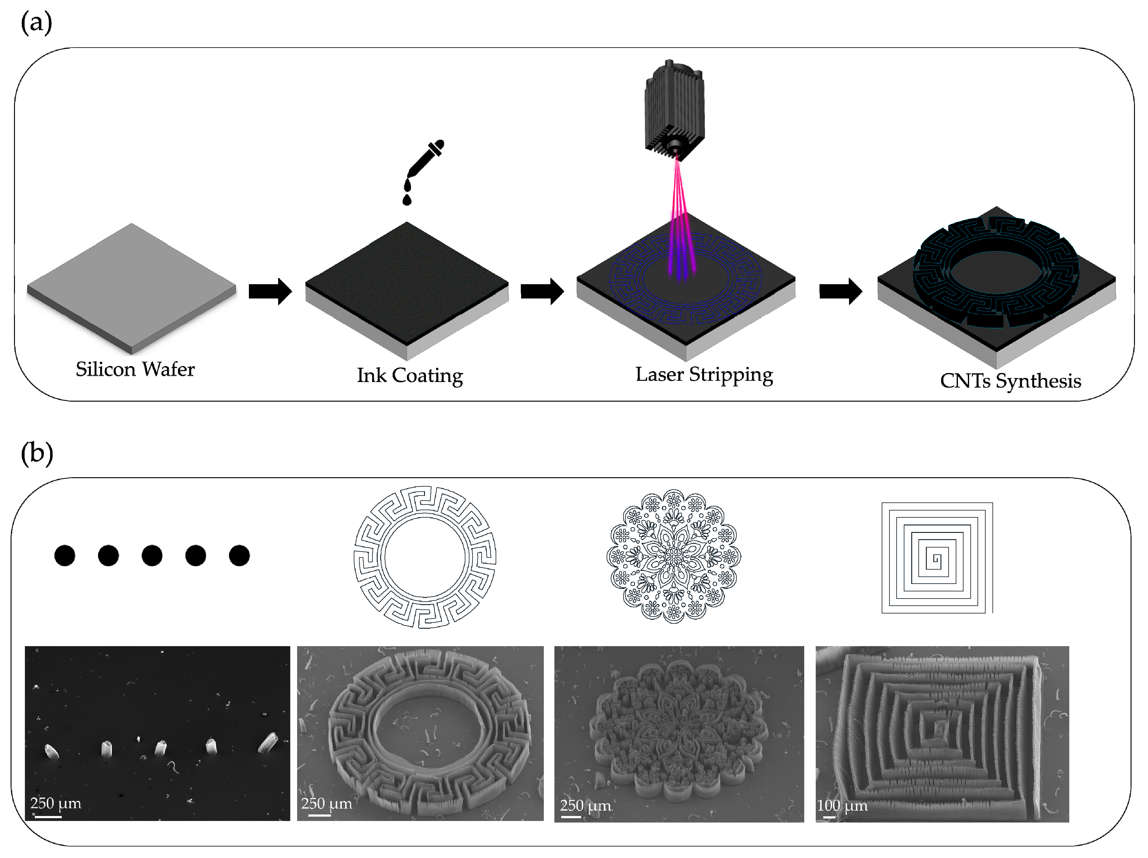
- If using a laser with a smaller spot size, the line width of the patterns could be reduced even further, resulting in an increase to the concentration of nanotube forest arrays and an improvement in application.
- The laser stripping method is equally applicable to thin and highly pliable materials, such as aluminum foil, as long as the parameters are adjusted properly so that the aluminum surface is not damaged when the ink is removed.
- Apart from SMA, we believe that there are other materials that could equally achieve the task of blocking CNT forest growth. Any polymer that does not carbonize under high heat and possesses high melt viscosity could be employed to achieve CNT patterning. As nanotube synthesis involves immense heat, materials with low viscosity and high fluidity could affect the overall integrity of the pattern.
Supplementary Materials
Author Contributions
Funding
Conflicts of Interest
References
- Wei, B.Q.; Vajtai, R.; Ajayan, P.M. Reliability and current carrying capacity of carbon nanotubes. Appl. Phys. Lett. 2001, 79, 1172–1174. [Google Scholar] [CrossRef]
- Baughman, R.H.; Zakhidov, A.A.; de Heer, W.A. Carbon nanotubes—The route toward applications. Science 2002, 297, 787–792. [Google Scholar] [CrossRef]
- De Volder, M.F.L.; Tawfick, S.H.; Baughman, R.H.; Hart, A.J. Carbon Nanotubes: Present and Future Commercial Applications. Science 2013, 339, 535–539. [Google Scholar] [CrossRef] [Green Version]
- Deheer, W.A.; Chatelain, A.; Ugarte, D. A Carbon Nanotube Field-Emission Electron Source. Science 1995, 270, 1179–1180. [Google Scholar] [CrossRef]
- Fan, S.S.; Chapline, M.G.; Franklin, N.R.; Tombler, T.W.; Cassell, A.M.; Dai, H.J. Self-oriented regular arrays of carbon nanotubes and their field emission properties. Science 1999, 283, 512–514. [Google Scholar] [CrossRef] [PubMed]
- Park, S.; Gupta, A.; Yeo, S.; Jung, J.; Paik, S.; Mativenga, M.; Kim, S.; Shin, J.; Ahn, J.; Ryu, J. Carbon nanotube field emitters synthesized on metal alloy substrate by PECVD for customized compact field emission devices to be used in X-ray source applications. Nanomaterials 2018, 8, 378. [Google Scholar] [CrossRef] [PubMed]
- Campo, T.; Pinilla, S.; Gálvez, S.; Sanz, J.M.; Márquez, F.; Morant, C. Synthesis Procedure of Highly Densely Packed Carbon Nanotube Forests on TiN. Nanomaterials 2019, 9, 571. [Google Scholar] [CrossRef] [PubMed]
- Kong, J.; Franklin, N.R.; Zhou, C.; Chapline, M.G.; Peng, S.; Cho, K.; Dai, H. Nanotube molecular wires as chemical sensors. Science 2000, 287, 622–625. [Google Scholar] [CrossRef]
- Qi, P.; Vermesh, O.; Grecu, M.; Javey, A.; Wang, Q.; Dai, H.; Peng, S.; Cho, K.J. Toward large arrays of multiplex functionalized carbon nanotube sensors for highly sensitive and selective molecular detection. Nano Lett. 2003, 3, 347–351. [Google Scholar] [CrossRef]
- Kam, N.W.S.; O’Connell, M.; Wisdom, J.A.; Dai, H.J. Carbon nanotubes as multifunctional biological transporters and near-infrared agents for selective cancer cell destruction. Proc. Natl. Acad. Sci. USA 2005, 102, 11600–11605. [Google Scholar] [CrossRef] [Green Version]
- Dai, H.; Hafner, J.H.; Rinzler, A.G.; Colbert, D.T.; Smalley, R.E. Nanotubes as nanoprobes in scanning probe microscopy. Nature 1996, 384, 147–150. [Google Scholar] [CrossRef]
- Hafner, J.H.; Cheung, C.L.; Lieber, C.M. Growth of nanotubes for probe microscopy tips. Nature 1999, 398, 761–762. [Google Scholar] [CrossRef] [Green Version]
- Nishijima, H.; Kamo, S.; Akita, S.; Nakayama, Y.; Hohmura, K.I.; Yoshimura, S.H.; Takeyasu, K. Carbon-nanotube tips for scanning probe microscopy: Preparation by a controlled process and observation of deoxyribonucleic acid. Appl. Phys. Lett. 1999, 74, 4061–4063. [Google Scholar] [CrossRef]
- Zhang, J.; Tang, J.; Yang, G.; Qiu, Q.; Qin, L.C.; Zhou, O. Efficient fabrication of carbon nanotube point electron sources by dielectrophoresis. Adv. Mater. 2004, 16, 1219–1222. [Google Scholar] [CrossRef]
- Slattery, A.; Shearer, C.; Shapter, J.; Quinton, J.; Gibson, C. Solution based methods for the fabrication of carbon nanotube modified atomic force microscopy probes. Nanomaterials 2017, 7, 346. [Google Scholar] [CrossRef] [PubMed]
- Hu, X.; Wei, H.; Deng, Y.; Chi, X.; Liu, J.; Yue, J.; Peng, Z.; Cai, J.; Jiang, P.; Sun, L. Amplitude response of conical multiwalled carbon nanotube probes for atomic force microscopy. RSC Adv. 2019, 9, 429–434. [Google Scholar] [CrossRef] [Green Version]
- Wong, H.P.; Appenzeller, J.; Derycke, V.; Martel, R.; Wind, S.; Avouris, P. Carbon nanotube field effect transistors—Fabrication, device physics, and circuit implications. In Proceedings of the 2003 IEEE International Solid-State Circuits Conference, San Francisco, CA, USA, 13 February 2003. [Google Scholar]
- Schroter, M.; Claus, M.; Sakalas, P.; Haferlach, M.; Wang, D. Carbon Nanotube FET Technology for Radio-Frequency Electronics: State-of-the-Art Overview. IEEE J. Electron Devices Soc. 2013, 1, 9–20. [Google Scholar] [CrossRef]
- Shulaker, M.M.; Hills, G.; Park, R.S.; Howe, R.T.; Saraswat, K.; Wong, H.S.; Mitra, S. Three-dimensional integration of nanotechnologies for computing and data storage on a single chip. Nature 2017, 547, 74. [Google Scholar] [CrossRef] [PubMed]
- Kong, J.; Soh, H.T.; Cassell, A.M.; Quate, C.F.; Dai, H.J. Synthesis of individual single-walled carbon nanotubes on patterned silicon wafers. Nature 1998, 395, 878–881. [Google Scholar] [CrossRef]
- Huang, S.M.; Mau, A.W.H.; Turney, T.W.; White, P.A.; Dai, L.M. Patterned growth of well-aligned carbon nanotubes: A soft-lithographic approach. J. Phys. Chem. B 2000, 104, 2193–2196. [Google Scholar] [CrossRef]
- Joachim, C.; Gimzewski, J.K.; Aviram, A. Electronics using hybrid-molecular and mono-molecular devices. Nature 2000, 408, 541–548. [Google Scholar] [CrossRef]
- Bachtold, A.; Hadley, P.; Nakanishi, T.; Dekker, C. Logic circuits with carbon nanotube transistors. Science 2001, 294, 1317–1320. [Google Scholar] [CrossRef] [PubMed]
- Franklin, N.R.; Li, Y.M.; Chen, R.J.; Javey, A.; Dai, H.J. Patterned growth of single-walled carbon nanotubes on full 4-inch wafers. Appl. Phys. Lett. 2001, 79, 4571–4573. [Google Scholar] [CrossRef] [Green Version]
- Javey, A.; Guo, J.; Wang, Q.; Lundstrom, M.; Dai, H.J. Ballistic carbon nanotube field-effect transistors. Nature 2003, 424, 654–657. [Google Scholar] [CrossRef] [PubMed]
- Tselev, A.; Hatton, K.; Fuhrer, M.S.; Paranjape, M.; Barbara, P. A photolithographic process for fabrication of devices with isolated single-walled carbon nanotubes. Nanotechnology 2004, 15, 1475–1478. [Google Scholar] [CrossRef]
- Edgeworth, J.P.; Wilson, N.R.; Macpherson, J.V. Controlled growth and characterization of two-dimensional single-walled carbon-nanotube networks for electrical applications. Small 2007, 3, 860–870. [Google Scholar] [CrossRef] [PubMed]
- Pander, A.; Hatta, A.; Furuta, H. FIB Secondary Etching Method for Fabrication of Fine CNT Forest Metamaterials. Nano-Micro Lett. 2017, 9, 44. [Google Scholar] [CrossRef]
- Lee, J.S.; Gu, G.H.; Kim, H.; Jeong, K.S.; Bae, J.; Suh, J.S. Growth of carbon nanotubes on anodic aluminum oxide templates: Fabrication of a tube-in-tube and linearly joined tube. Chem. Mater. 2001, 13, 2387–2391. [Google Scholar] [CrossRef]
- Wang, Q.H.; Corrigan, T.D.; Dai, J.Y.; Chang, R.P.H.; Krauss, A.R. Field emission from nanotube bundle emitters at low fields. Appl. Phys. Lett. 1997, 70, 3308–3310. [Google Scholar] [CrossRef]
- Liu, Y.M.; Liu, L.; Liu, P.; Sheng, L.M.; Fan, S.S. Plasma etching carbon nanotube arrays and the field emission properties. Diam. Relat. Mater. 2004, 13, 1609–1613. [Google Scholar] [CrossRef]
- Cheng, H.M.; Li, F.; Su, G.; Pan, H.Y.; He, L.L.; Sun, X.; Dresselhaus, M.S. Large-scale and low-cost synthesis of single-walled carbon nanotubes by the catalytic pyrolysis of hydrocarbons. Appl. Phys. Lett. 1998, 72, 3282–3284. [Google Scholar] [CrossRef]
- Moisala, A.; Nasibulin, A.G.; Kauppinen, E.I. The role of metal nanoparticles in the catalytic production of single-walled carbon nanotubes—A review. J. Phys. Condens. Matter 2003, 15, S3011–S3035. [Google Scholar] [CrossRef]
- Coman, V.; Copaciu, F. Analysis of Dyes and Inks. In Instrumental Thin-Layer Chromatography; Poole, C.F., Ed.; Elsevier: Boston, MA, USA, 2015; Chapter 20; pp. 555–588. [Google Scholar]
- Niaounakis, M. Inks. In Biopolymers: Processing and Products; Niaounakis, M., Ed.; William Andrew Publishing: Oxford, UK, 2015; Chapter 14; pp. 447–458. [Google Scholar]
- Schmidhauser, J.C.T.; Hahn, L.M. SMA Resin Amic Acids. U.S. Patent 6,232,405, 15 May 2001. [Google Scholar]
- Gore, R.H.S.; Langenmayr, E.J.; Machleder, W.H.; Lorah, D.P.; Van Dyk, A.K.; Bortnick, N.M. Colorants, Dispersants, Dispersions, and Inks. U.S. Patent 20030055178, 20 March 2003. [Google Scholar]
- Guo, D.Z.S.D.; Chen, X. Ink System Containing Polymer Binders. U.S. Patent 8,946,320, 3 February 2015. [Google Scholar]
- Su, J.F.; Wang, S.B.; Zhang, Y.Y.; Huang, Z. Physicochemical properties and mechanical characters of methanol-modified melamine-formaldehyde (MMF) shell microPCMs containing paraffin. Colloid Polym. Sci. 2011, 289, 111–119. [Google Scholar] [CrossRef]
- Su, J.F.; Wang, S.B.; Zhou, J.W.; Huang, Z.; Zhao, Y.H.; Yuan, X.Y.; Zhang, Y.Y.; Kou, J.B. Fabrication and interfacial morphologies of methanol-melamine-formaldehyde (MMF) shell microPCMs/epoxy composites. Colloid Polym. Sci. 2011, 289, 169–177. [Google Scholar] [CrossRef]


© 2019 by the authors. Licensee MDPI, Basel, Switzerland. This article is an open access article distributed under the terms and conditions of the Creative Commons Attribution (CC BY) license (http://creativecommons.org/licenses/by/4.0/).
Share and Cite
Li, Y.-R.; Huang, C.-P.; Su, C.-C.; Chang, S.-H. Ultrafast Patterning Vertically Aligned Carbon Nanotube Forest on Al Foil and Si Substrate Using Chemical Vapor Deposition (CVD). Nanomaterials 2019, 9, 1332. https://doi.org/10.3390/nano9091332
Li Y-R, Huang C-P, Su C-C, Chang S-H. Ultrafast Patterning Vertically Aligned Carbon Nanotube Forest on Al Foil and Si Substrate Using Chemical Vapor Deposition (CVD). Nanomaterials. 2019; 9(9):1332. https://doi.org/10.3390/nano9091332
Chicago/Turabian StyleLi, Yan-Rui, Chin-Ping Huang, Chih-Chung Su, and Shuo-Hung Chang. 2019. "Ultrafast Patterning Vertically Aligned Carbon Nanotube Forest on Al Foil and Si Substrate Using Chemical Vapor Deposition (CVD)" Nanomaterials 9, no. 9: 1332. https://doi.org/10.3390/nano9091332