Dynamics Contributions to the Growth Mechanism of Ga2O3 Thin Film and NWs Enabled by Ag Catalyst


Abstract
1. Introduction
2. Materials and Methods
3. Results & Discussion
3.1. X-ray Diffraction
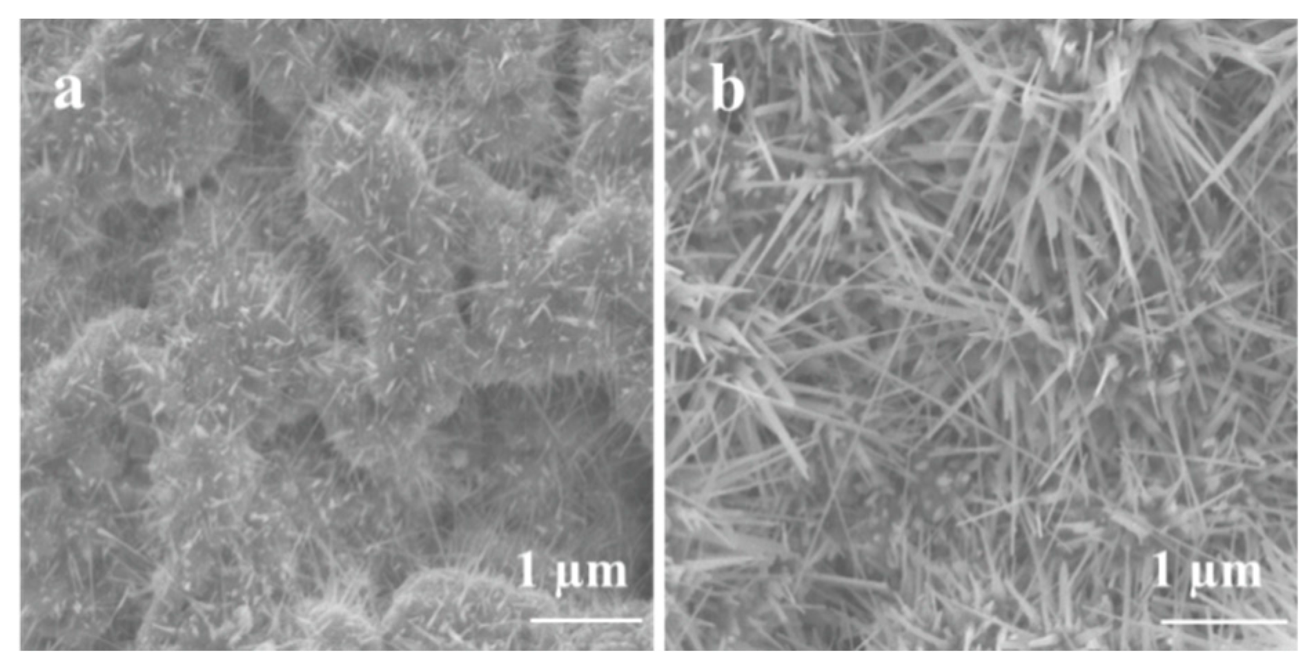
3.2. SEM Characterization
3.3. FIB/EDS Characterization
3.4. Scanning Transmission Electron Microscopy (STEM)
3.5. Factors Effecting the Ga2O3 Growth
- Silver Thin Film Thickness
- Oxidation Temperature
- Oxygen Concentration
- Oxidation Time
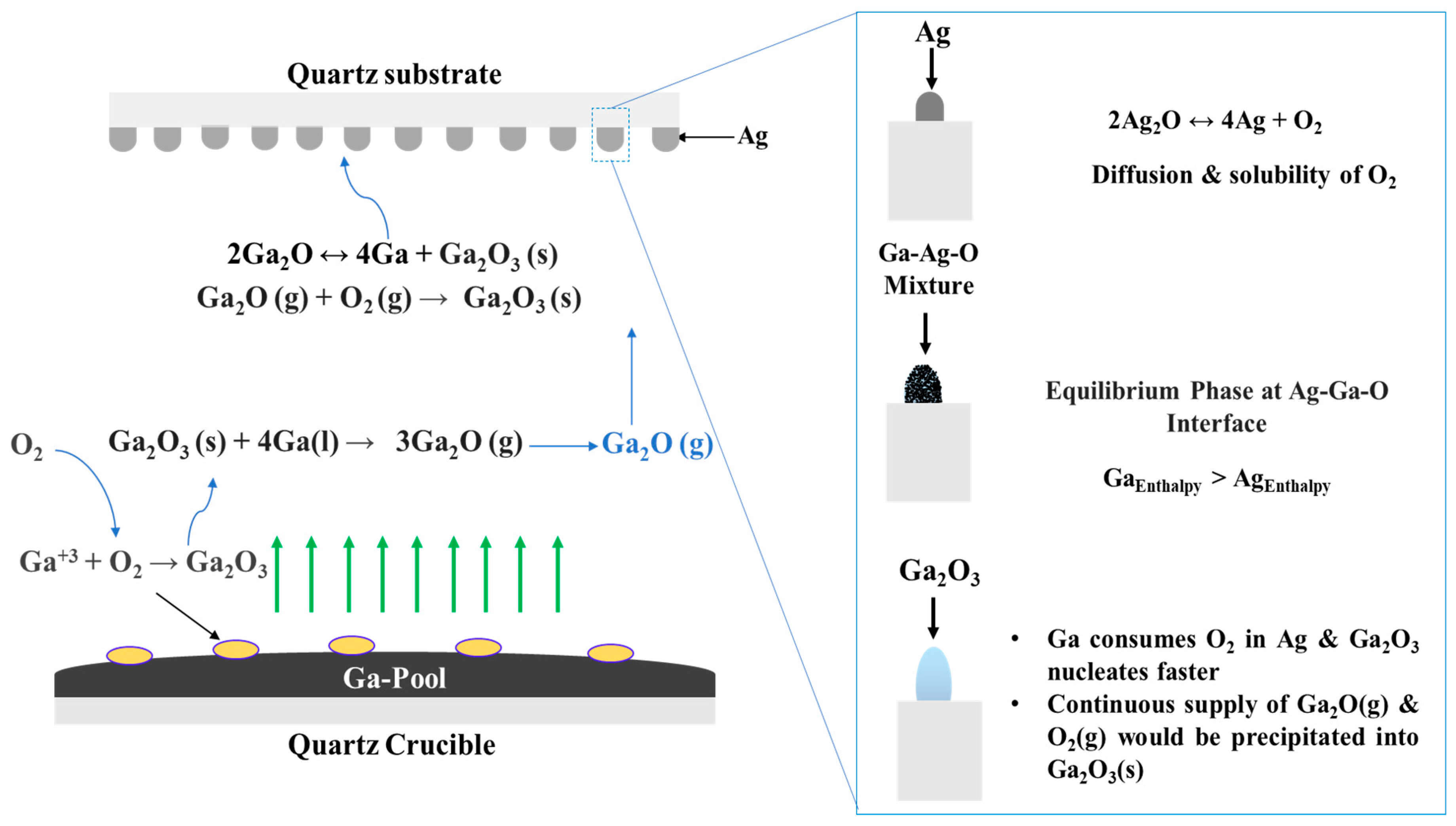
- Growth Mechanism
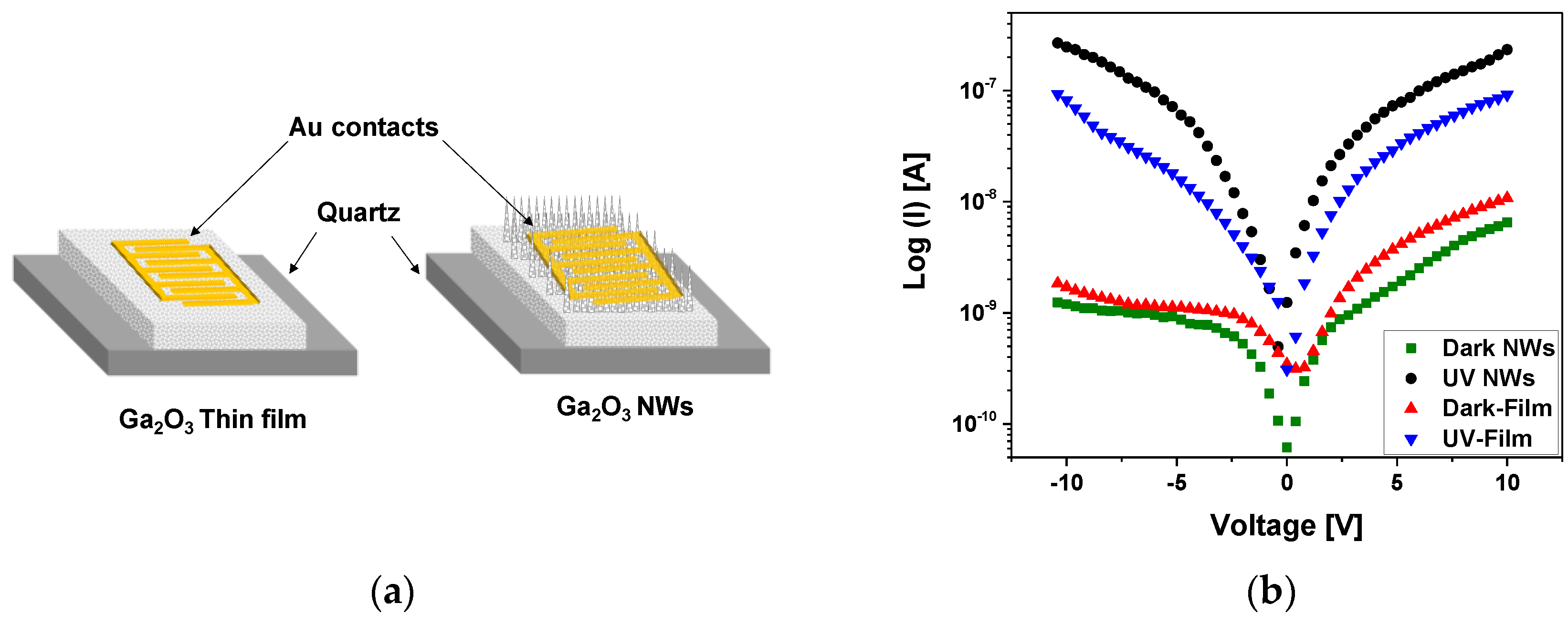
- Electrical Properties of the Ga2O3 Film and Nanowires
4. Conclusions
Author Contributions
Funding
Acknowledgments
Conflicts of Interest
References
- Lin, H.-J.; Baltrus, J.P.; Gao, H.; Ding, Y.; Nam, C.-Y.; Ohodnicki, P.; Gao, P.-X. Perovskite Nanoparticle-Sensitized Ga2O3 Nanorod Arrays for CO Detection at High Temperature. ACS Appl. Mater. Interfaces 2016, 8, 8880–8887. [Google Scholar] [CrossRef] [PubMed]
- Kaya, A.; Mao, H.; Gao, J.; Chopdekar, R.V.; Takamura, Y.; Chowdhury, S.; Islam, M.S. An Investigation of Electrical and Dielectric Parameters of Sol-Gel Process Enabled beta-Ga2O3 as a Gate Dielectric Material. IEEE Trans. Electron Devices 2017, 64, 2047–2053. [Google Scholar] [CrossRef]
- Grillo, A.; Barrat, J.; Galazka, Z.; Passacantando, M.; Giubileo, F.; Iemmo, L.; Luongo, G.; Urban, F.; Dubourdieu, C.; Di Bartolomeo, A. High field-emission current density from β-Ga2O3 nanopillars. Appl. Phys. Lett. 2019, 114, 193101. [Google Scholar] [CrossRef]
- Pearton, S.J.; Yang, J.; Cary, P.H.; Ren, F.; Kim, J.; Tadjer, M.J.; Mastro, M.A. A review of Ga2O3 materials, processing, and devices. Appl. Phys. Rev. 2018, 5, 011301. [Google Scholar] [CrossRef]
- Kaya, A.; Dryden, D.M.; Woodall, J.M.; Islam, M.S. Spontaneous delamination via compressive buckling facilitates large-scale-Ga2O3 thin film transfer from reusable GaAs substrates. Phys. Status Solidi Appl. Mater. Sci. 2017, 214, 1700102. [Google Scholar] [CrossRef]
- Alhalaili, B.; Mao, H.; Islam, S. Ga2O3 Nanowire Synthesis and Device Applications. In Novel Nanomaterials—Synthesis and Applications; Kyzas, G.Z., Mitropoulos, A.C., Eds.; IntechOpen: London, UK, 2017. [Google Scholar] [CrossRef]
- Patil-Chaudhari, D.; Ombaba, M.; Oh, J.Y.; Mao, H.; Montgomery, K.H.; Lange, A.; Mahajan, S.; Woodall, J.M.; Islam, M.S. Solar Blind Photodetectors Enabled by Nanotextured beta-Ga2O3 Films Grown via Oxidation of GaAs Substrates. IEEE Photonics J. 2017, 9, 1–7. [Google Scholar] [CrossRef]
- Bayam, Y.; Logeeswaran, V.J.; Katzenmeyer, A.M.; Sadeghian, R.B.; Chacon, R.J.; Wong, M.C.; Hunt, C.E.; Motomiya, K.; Jeyadevan, B.; Islam, M.S. Synthesis of Ga2O3 Nanorods with Ultra-Sharp Tips for High-Performance Field Emission Devices. Sci. Adv. Mater. 2015, 7, 211–218. [Google Scholar] [CrossRef][Green Version]
- Nguyen, T.D.; Kim, E.T.; Dao, K.A. Ag nanoparticle catalyst based on Ga2O3/GaAs semiconductor nanowire growth by VLS method. J. Mater. Sci. Mater. Electron. 2015, 26, 8747–8752. [Google Scholar] [CrossRef]
- Guo, D.; Wu, Z.; Li, P.; Wang, Q.; Lei, M.; Li, L.; Tang, W. Magnetic anisotropy and deep ultraviolet photoresponse characteristics in Ga2O3: Cr vermicular nanowire thin film nanostructure. RSC Adv. 2015, 5, 12894–12898. [Google Scholar] [CrossRef]
- Lee, S.Y.; Choi, K.H.; Kang, H.C. Growth mechanism of In-doped beta-Ga2O3 nanowires deposited by radio frequency powder sputtering. Mater. Lett. 2016, 176, 213–218. [Google Scholar] [CrossRef]
- Choi, K.-H.; Cho, K.-K.; Kim, K.-W.; Cho, G.-B.; Ahn, H.-J.; Nam, T.-H. Catalytic Growth and Structural Characterization of Semiconducting beta-Ga2O3 Nanowires. J. Nanosci. Nanotechnol. 2009, 9, 3728–3733. [Google Scholar] [CrossRef] [PubMed]
- Park, S.; Sun, G.J.; Lee, C. UV-assisted room temperature-gas sensing of Ga2O3-core/ZnO-shell nanowires. J. Ceram. Process. Res. 2015, 16, 367–371. [Google Scholar]
- Jang, Y.-G.; Kim, W.-S.; Kim, D.-H.; Hong, S.-H. Fabrication of Ga2O3/SnO2 core-shell nanowires and their ethanol gas sensing properties. J. Mater. Res. 2011, 26, 2322–2327. [Google Scholar] [CrossRef]
- Ghose, S.; Rahman, S.M.; Arias, A.; Rojas-Ramirez, J. Structural and optical properties of beta-Ga2O3 thin films grown by plasma-assisted molecular beam epitaxy. J. Vac. Sci. Technol. B 2016, 34, 02L109. [Google Scholar] [CrossRef]
- Feng, Q.; Li, F.; Dai, B.; Jia, Z.; Xie, W.; Xu, T.; Lu, X.; Tao, X.; Zhang, J.; Hao, Y. The properties of gallium oxide thin film grown by pulsed laser deposition. Appl. Surf. Sci. 2015, 359, 847–852. [Google Scholar] [CrossRef]
- Han, W.; Kohler-Redlich, P.; Ernst, F.; Rühle, M. Growth and microstructure of Ga2O3 nanorods. Solid State Commun. 2000, 115, 527–529. [Google Scholar] [CrossRef]
- Cao, C.B.; Chen, Z.; An, X.Q.; Zhu, H.S. Growth and field emission properties of cactus-like gallium oxide nanostructures. J. Phys. Chem. C 2008, 112, 95–98. [Google Scholar] [CrossRef]
- Sharma, S.; Sunkara, M.K. Direct synthesis of gallium oxide tubes, nanowires, and nanopaintbrushes. J. Am. Chem. Soc. 2002, 124, 12288–12293. [Google Scholar] [CrossRef]
- Pallister, P.J.; Buttera, S.C.; Barry, S.T. Self-seeding gallium oxide nanowire growth by pulsed chemical vapor deposition. Phys. Status Solidi Appl. Mater. Sci. 2015, 212, 1514–1518. [Google Scholar] [CrossRef]
- Zhao, Y.; Frost, R.L.; Yang, J.; Martens, W.N. Size and morphology control of gallium oxide hydroxide GaO(OH), nano- to micro-sized particles by soft-chemistry route without surfactant. J. Phys. Chem. C 2008, 112, 3568–3579. [Google Scholar] [CrossRef]
- Reddy, L.S.; Ko, Y.H.; Yu, J.S. Hydrothermal Synthesis and Photocatalytic Property of beta-Ga2O3 Nanorods. Nanoscale Res. Lett. 2015, 10, 364. [Google Scholar] [CrossRef] [PubMed]
- Mao, H.; Alhalaili, B.; Kaya, A.; Dryden, D.M.; Woodall, J.M.; Islam, M.S. Oxidation of GaAs Substrates to Enable β-Ga2O3 Films for Sensors and Optoelectronic Devices (SPIE Optical Engineering + Applications); SPIE: San Diego, CA, USA, 2017. [Google Scholar]
- Yoshida, T.; Yamamoto, N.; Mizutani, T.; Yamamoto, M.; Ogawa, S.; Yagi, S.; Nameki, H.; Yoshida, H. Synthesis of Ag nanoparticles prepared by a solution plasma method and application as a cocatalyst for photocatalytic reduction of carbon dioxide with water. Catal. Today 2018, 303, 320–326. [Google Scholar] [CrossRef]
- Arora, K.; Kumar, V.; Kumar, M. Silver plasmonic density tuned polarity switching and anomalous behaviour of high performance self-powered β-gallium oxide solarblind photodetector. Appl. Phys. Lett. 2018, arXiv:1809.10724. [Google Scholar]
- omer, V.K.; Malik, R.; Chaudhary, V.; Mishra, Y.K.; Kienle, L.; Ahuja, R.; Lin, L. Superior visible light photocatalysis and low-operating temperature VOCs sensor using cubic Ag(0)-MoS2 loaded g-CN 3D porous hybrid. Appl. Mater. Today 2019, 16, 193–203. [Google Scholar]
- Tomer, V.K.; Duhan, S. A facile nanocasting synthesis of mesoporous Ag-doped SnO2 nanostructures with enhanced humidity sensing performance. Sens. Actuators B Chem. 2016, 223, 750–760. [Google Scholar] [CrossRef]
- Tomer, V.K.; Duhan, S. Ordered mesoporous Ag-doped TiO2/SnO2 nanocomposite based highly sensitive and selective VOC sensors. J. Mater. Chem. A 2016, 4, 1033–1043. [Google Scholar] [CrossRef]
- Zhao, Y.Y.; Frost, R.L. Raman spectroscopy and characterisation of alpha-gallium oxyhydroxide and beta-gallium oxide nanorods. J. Raman Spectrosc. 2008, 39, 1494–1501. [Google Scholar] [CrossRef]
- Askeland, D.R.; Fulay, P.P.; Wright, W.J. The Science and Engineering of Materials; SI Edition; CL-Engineering: Stamford, CT, USA, 2011; p. 944. [Google Scholar]
- Yang, S.M.; Kim, S.R.N.; Youn, W.K.; Kim, C.S.; Kim, D.S.; Yi, K.W.; Hwang, N.M. Generation of Charged Nanoparticles During Thermal Evaporation of Silver at Atmospheric Pressure. J. Nanosci. Nanotechnol. 2015, 15, 8418–8423. [Google Scholar] [CrossRef] [PubMed]
- Müller, C.M.; Spolenak, R. Microstructure evolution during dewetting in thin Au films. Acta Mater. 2010, 58, 6035–6045. [Google Scholar] [CrossRef]
- Strobel, S.; Kirkendall, C.; Chang, J.-B.; Berggren, K.K. Sub-10 nm structures on silicon by thermal dewetting of platinum. Nanotechnology 2010, 21, 505301. [Google Scholar] [CrossRef]
- Nsimama, P.D. Morphological and Structural Properties of Silver Nanofilms Annealed by RTP in Different Atmospheres. Am. J. Nano Res. Appl. 2015, 3, 99–104. [Google Scholar]
- Lindberg, C.; Whiticar, A.; Dick, K.A.; Sköld, N.; Nygård, J.; Bolinsson, J. Silver as Seed-Particle Material for GaAs Nanowires-Dictating Crystal Phase and Growth Direction by Substrate Orientation. Nano Lett. 2016, 16, 2181–2188. [Google Scholar] [CrossRef] [PubMed]
- Han, C.Q.; Mao, W.T.; Bao, K.Y.; Xie, H.Q.; Jia, Z.Y.; Ye, L.Q. Preparation of Ag/Ga2O3 nanofibers via electrospinning and enhanced photocatalytic hydrogen evolution. Int. J. Hydrog. Energy 2017, 42, 19913–19919. [Google Scholar] [CrossRef]
- Zhou, Z.-Y.; Ma, Y.; Han, Q.-F.; Liu, Y.-L. Solubility, permeation, and capturing of impurity oxygen in Au/Ag: A comparative investigation from first-principles. Comput. Mater. Sci. 2016, 114, 79–85. [Google Scholar] [CrossRef]
- Yasui, K.; Kohiki, S.; Shimooka, H.; Shishido, T. Effects of Au catalyst on growth of beta-Ga2O3 nanostructure at alpha-Al2O3 (0001) surface. Solid State Sci. 2008, 10, 1860–1863. [Google Scholar] [CrossRef]
- Kim, H.W.; Kim, N.H. Synthesis of beta-Ga2O3 nanowires by an MOCVD approach. Appl. Phys. Mater. Sci. Process. 2005, 81, 763–765. [Google Scholar] [CrossRef]
- Kumar, S.; Sarau, G.; Tessarek, C.; Bashouti, M.; Hähnel, A.; Christiansen, S.; Singh, R. Study of iron-catalysed growth of beta-Ga2O3 nanowires and their detailed characterization using TEM, Raman and cathodoluminescence techniques. J. Phys. D Appl. Phys. 2014, 47, 435101. [Google Scholar] [CrossRef]
- Song, P.Y.; Wu, Z.Y.; Shen, X.Y.; Kang, J.Y.; Fang, Z.L.; Zhang, T.Y. Self-consistent growth of single-crystalline ((2)over-bar01)beta-Ga2O3 nanowires using a flexible GaN seed nanocrystal. CrystEngComm 2017, 19, 625–631. [Google Scholar] [CrossRef]
- Hajakbari, F.; Ensandoust, M. Study of Thermal Annealing Effect on the Properties of Silver Thin Films Prepared by DC Magnetron Sputtering. Acta Phys. Pol. A 2016, 129, 680–682. [Google Scholar] [CrossRef]
- Zinkevich, M.; Aldinger, F. Thermodynamic assessment of the gallium-oxygen system. J. Am. Ceram. Soc. 2004, 87, 683–691. [Google Scholar] [CrossRef]
- Tollefson, E.L.; Cambron, A.; Smeltzer, W.W. Adsorption of Oxygen by a Silver Catalyst. Can. J. Chem. Rev. Can. Chim. 1956, 34, 1046–1060. [Google Scholar]
- Zhu, F.; Yang, Z.X.; Zhou, W.M.; Zhang, Y.F. Direct synthesis of beta gallium oxide nanowires, nanobelts, nanosheets and nanograsses by microwave plasma. Solid State Commun. 2006, 137, 177–181. [Google Scholar] [CrossRef]
- Sajanlal, P.R.; Sreeprasad, T.S.; Samal, A.K.; Pradeep, T. Anisotropic nanomaterials: Structure, growth, assembly, and functions. Nano Rev. 2011, 2, 5883. [Google Scholar] [CrossRef] [PubMed]
- Shao, D.; Yu, M.; Sun, H.; Hu, T.; Lian, J.; Sawyer, S. High responsivity, fast ultraviolet photodetector fabricated from ZnO nanoparticle-graphene core-shell structures. Nanoscale 2013, 5, 3664–3667. [Google Scholar] [CrossRef] [PubMed]
- Weng, W.Y.; Hsueh, T.J.; Chang, S.J.; Huang, G.J.; Hsueh, H.T. A beta-Ga2O3 Solar-Blind Photodetector Prepared by Furnace Oxidization of GaN Thin Film. IEEE Sens. J. 2011, 11, 999–1003. [Google Scholar] [CrossRef]


© 2019 by the authors. Licensee MDPI, Basel, Switzerland. This article is an open access article distributed under the terms and conditions of the Creative Commons Attribution (CC BY) license (http://creativecommons.org/licenses/by/4.0/).
Share and Cite
Alhalaili, B.; Bunk, R.; Vidu, R.; Islam, M.S. Dynamics Contributions to the Growth Mechanism of Ga2O3 Thin Film and NWs Enabled by Ag Catalyst. Nanomaterials 2019, 9, 1272. https://doi.org/10.3390/nano9091272
Alhalaili B, Bunk R, Vidu R, Islam MS. Dynamics Contributions to the Growth Mechanism of Ga2O3 Thin Film and NWs Enabled by Ag Catalyst. Nanomaterials. 2019; 9(9):1272. https://doi.org/10.3390/nano9091272
Chicago/Turabian StyleAlhalaili, Badriyah, Ryan Bunk, Ruxandra Vidu, and M. Saif Islam. 2019. "Dynamics Contributions to the Growth Mechanism of Ga2O3 Thin Film and NWs Enabled by Ag Catalyst" Nanomaterials 9, no. 9: 1272. https://doi.org/10.3390/nano9091272
APA StyleAlhalaili, B., Bunk, R., Vidu, R., & Islam, M. S. (2019). Dynamics Contributions to the Growth Mechanism of Ga2O3 Thin Film and NWs Enabled by Ag Catalyst. Nanomaterials, 9(9), 1272. https://doi.org/10.3390/nano9091272