Precise Layer Control of MoTe2 by Ozone Treatment


State Key Laboratory of ASIC & System, School of Information Science and Technology, Fudan University, Shanghai 200433, China
*
Authors to whom correspondence should be addressed.
Nanomaterials 2019, 9(5), 756; https://doi.org/10.3390/nano9050756
Submission received: 23 April 2019
/
Revised: 9 May 2019
/
Accepted: 15 May 2019
/
Published: 17 May 2019
Abstract
:Transition metal dichalcogenides (TMDCs) demonstrate great potential in numerous applications. However, these applications require a precise control of layer thickness at the atomic scale. In this work, we present an in-situ study of the self-limiting oxidation process in MoTe2 by ozone (O3) treatment. A precise layer-by-layer control of MoTe2 flakes can be achieved via multiple cycles of oxidation and wet etching. The thinned MoTe2 flakes exhibit comparable optical properties and film quality to the pristine exfoliated ones. Besides, an additional p-type doping is observed after O3 oxidation. Such a p-doping effect converts the device properties of MoTe2 from electron-dominated to hole-dominated ambipolar characteristics.
1. Introduction
The past decade has witnessed a rapid development in two-dimensional (2D) materials research with a focus on the family of transition metal dichalcogenides (TMDCs) [1,2,3]. Depending on polytype and the number of transition metal d-electrons, TMDC materials exhibit a wide range of electronic properties, from semiconducting, metallic, to superconducting [1]. These unique electrical and optical properties are highly thickness dependent. Two-dimensional materials like MoS2, MoSe2, and their tungsten analogs, with their indirect bandgap transformed to direct in the monolayer limit [4,5,6], could be used as promising candidates for applications in electronics and optoelectronics [7,8,9].
The direct bandgap depends on the chalcogen species chosen in TMDCs. Compared with other TMDC materials, monolayer MoTe2 has a direct bandgap of 1.1 eV, which is the smallest among all semiconducting TMDCs [10,11]. MoTe2 is thought to be an ideal candidate to bridge large-bandgap TMDCs and gapless graphene. Because its bandgap is comparable to that of silicon, MoTe2 can potentially expand the range of TMDC optoelectronic applications beyond the visible spectrum. In contrast to most TMDCs that exhibit indirect bandgaps in multilayer/bulk forms, MoTe2 still preserves its direct bandgap feature in bilayers, and perhaps even in trilayers with less change in bandgap value [12]. Furthermore, the narrow bandgap of MoTe2 facilitates the construction of n- and p-type transistors due to low Schottky barrier heights (SBHs) for electrons and holes [13]. In this regard, field effect transistors (FETs) built from MoTe2 have been demonstrated to display n-type, p-type, and ambipolar behaviors [14,15,16,17,18].
Since the electronic properties of 2D materials are highly dependent on the layer number, a simple and efficient method to precisely control layer thickness is a prerequisite for various applications. So far, several strategies have been established to prepare 2D TMDCs with a certain layer thickness, which can be generally categorized into top-down and bottom-up technologies. The top-down methods normally involve mechanical [19] and solution-based exfoliation [20] from bulk materials. Exfoliation-based techniques are very common, but typically generate flakes with random sizes and thicknesses. On the other hand, the bottom-up method usually yields 2D materials via chemical reactions of atoms/molecules on a substrate with a large power consumption [21].
In comparison, the post-treatment of multilayer materials is an alternative route to accurately control the layer number. Various layer-thinning technologies have been conducted, such as laser thinning [22], thermal annealing [23], and plasma etching [24]. TMDCs are known to potentially oxidize in ambient environments. This oxidation process is self-limiting to some degree, since the surface oxide film hinders oxygen diffusion into the underlying layers [25]. However, higher operating/processing temperatures enhance oxygen diffusion and accelerate the oxidation process. This leads to more layers being oxidized simultaneously and to lack a precise control over the number of layers. Hence, a fast reaction between the oxidizing agents and the surface layer, accompanied by a slow diffusion rate to the underlying layers, is expected to be a promising route to achieve controlled layer-by-layer thinning at the atomic scale. Compared with other oxidizing agents, ozone (O3) is a strong oxidant, which is unstable and easily decomposes into molecular O2 and monatomic O when reaching a solid surface; the latter is regarded as a main active species that vigorously reacts with TDMCs or other 2D materials [26,27,28]. Herein, we performed an in-situ study of O3 exposure of MoTe2 to monitor the evolution of layer number and characterize the quality of the thinned layers. A precise layer-by-layer control of MoTe2 layers was achieved via the cyclical processing of oxidation and subsequent removal of the oxidized layer. The thinned MoTe2 flakes exhibited comparable optical properties to the pristine exfoliated ones, and showed a p-type doping behavior.
2. Materials and Methods
MoTe2 flakes were mechanically exfoliated from bulk 2H-MoTe2 crystals (2D Semiconductors, Inc., Scottsdale, AZ, USA) and then deposited on a heavily p-doped Si substrate with a 300-nm-thick oxide layer. The thickness of the MoTe2 flakes was first identified using an optical microscope (VHX-600, Keyence, Inc., Itasca, IL, USA) through optical contrast and then further confirmed by atomic force microscopy (AFM, Dimension 3100, Veeco, Inc., New York, NY, USA) and Raman spectroscopy (Renishaw inVia, Renishaw, Inc., Gloucestershire, UK). Raman spectra were collected in a backscattering geometry with a 633 nm laser, 100× objective, and 1800 lines/mm grating. The laser power was kept below 0.1 mW to avoid sample damage.
Afterward, MoTe2 flakes were placed in a custom-designed container for in-situ Raman investigation. O3 was remotely generated by electric discharge with an O3 generator (M-600, Tonglin, Inc., Beijing, China) at an O2 pressure of 0.3 bar and then introduced to the chamber. The oxidized samples were immersed in KOH solution to remove the surface oxide and washed with deionized water. The chemical states of the MoTe2 specimen before/after O3 oxidization and after KOH treatment were characterized by X-ray photoelectron spectroscopy (XPS, Thermo Scientific Escalab 250Xi, Thermo Fisher Scientific, Inc., Waltham, MA, USA) using a monochromatic Al Kα X-ray source with a 100 μm spot size.
For electrical characterization, a back-gated MoTe2 FET device was fabricated on a SiO2/Si substrate. Multilayer MoTe2 was first transferred onto the substrate. The electrode patterns were defined by standard electron-beam lithography (JBX-6300FS, JEOL, Inc., Tokyo, Japan). A bilayer stack of Cr (5 nm)/Au (50 nm) was deposited by thermal evaporation on the flake to form source/drain electrodes. A lift-off process was then performed in acetone and isopropanol to complete the device fabrication. Multiple cycles of O3 oxidation and oxide layer removal were repeated on the MoTe2 channel to achieve layer-by-layer thinning. After each thinning cycle, the same device was characterized with a semiconductor parameter analyzer (B1500A, Agilent Inc., Santa Clara, CA, USA).
3. Results and Discussion
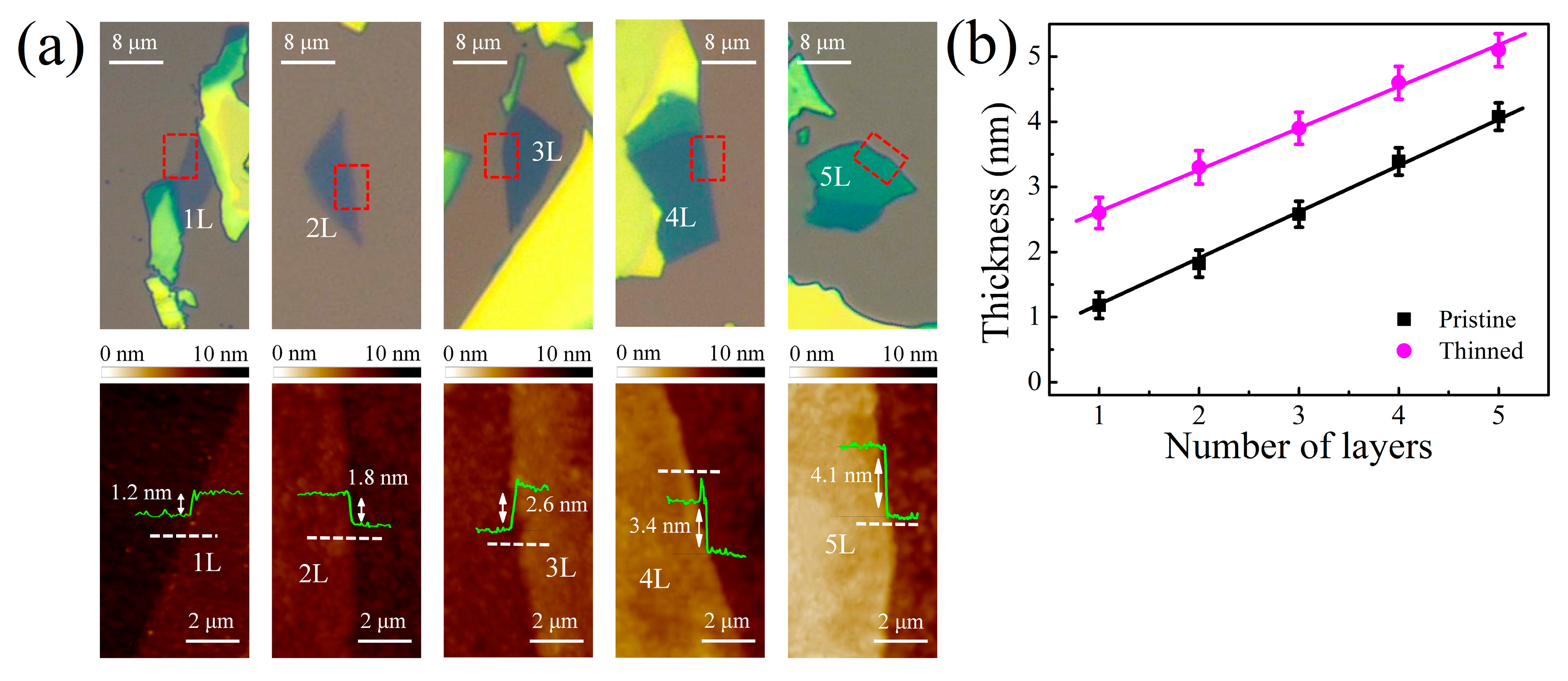
Figure 1a shows the optical microscope images and the corresponding AFM images of pristine MoTe2 with different layer numbers varying from monolayer to pentalayer. The number of layers and the corresponding thickness were first estimated from optical contrast and then further determined by AFM and Raman scattering. Obviously, the optical contrast of MoTe2 increases with the layer number due to the interference effect [29]. AFM height profiles of different layers are superimposed in the AFM images. A linear dependence of the layer thickness is observed with the layer number in Figure 1b. The interlayer distance was approximately 0.7 nm, which is in good agreement with the bulk interlayer spacing of MoTe2 [30]. Figure 2a shows the Raman spectra of MoTe2 flakes with several characteristic peaks between 150 and 300 cm−1. The peaks located at ~170, 230, and 290 cm−1 correspond to the out-of-plane mode A1g/A1’ (A1’ for odd layers and A1g for even layers), the in-plane mode E2g1, and the bulk-inactive mode B2g, respectively [31,32]. The B2g peak also vanished in monolayer (1L) but became active in few-layer MoTe2 due to translation symmetry breaking [33]. This can be a landmark to distinguish monolayers from few layers. Furthermore, the intensity of the B2g peak was sensitive to the thickness. As shown in Figure 2b, the peak intensity ratio of B2g to E2g1 consistently decreased with the layer number. This ratio can therefore be used to identify the number of MoTe2 layers, like the frequency difference between the A1g and E2g1 modes utilized in MoS2. Different from MoS2, the interlayer interactions also caused a Davydov splitting of A1g/A1’ modes in MoTe2 at thicknesses larger than bilayer [34].
After carefully characterizing the pristine exfoliated MoTe2, an in-situ Raman study of O3 exposure was performed to monitor the time evolution of the Raman spectra of MoTe2 during oxidation. First, a monolayer MoTe2 surface was exposed to the O3 for 70 s. As shown in Figure 3a,b, the peak intensities of the A1’ and E2g1 modes decreased with exposure time and completely disappeared in 25 s. The absence of Raman signals after the O3 treatment indicates that MoTe2 was fully oxidized. In contrast, under the same oxidation conditions, the A1g peak of bilayer MoTe2 became more prominent relative to the E2g1 mode with oxidation time (Figure 3c). Simultaneously, the characteristic B2g peak gradually disappeared with only A1g and E2g1 modes remaining. This suggests that bilayer MoTe2 was transformed into monolayer. Furthermore, the A1g peak intensity reached a maximum and remained nearly invariant after 25 s oxidation time (Figure 3d). However, the O3 oxidation of MoTe2 could proceed if UV illumination were introduced [28]. This hints that pure O3 exposure leads to a dense coverage of surface oxide layer on atomically thin MoTe2. The AFM images and the height profiles in Figure 4 show that the bilayer thickness increased by 1.5 nm after oxidation. This surface oxide layer suppressed the further diffusion of the oxygen atoms into the flake and their oxidation of the underlying layers, even with longer exposure times. This oxidation process was therefore self-limiting. Notably, the time to fully oxidize the monolayer and the top layer of MoTe2 flakes was almost the same, irrespective of layer numbers.
In order to realize a controllable layer-by-layer thinning of multilayer flakes, the surface oxide layer in MoTe2 needs to be removed and the underlying layer freshly exposed to provide a new surface to be reacted with O3. Generally, base (OH−) solutions are good solvents for metal oxides. Herein, an oxidized thick MoTe2 sample was immersed in KOH solution followed by a deionized water rinse. Afterward, XPS analysis was conducted on the MoTe2 to investigate the evolution of the surface chemical compositions before and after KOH solution immersion. As shown in Figure 5a, two dominant peaks in pristine MoTe2 were assigned to the Mo4+ 3d3/2 (231.7 eV) and 3d5/2 (228.5 eV) [35]. Te2− 3d3/2 and 3d5/2 were located at 583.5 and 573.2 eV, respectively (Figure 5b). However, after O3 treatment, the binding energies of Mo4+ and Te2− peaks were both red-shifted by approximately 0.4 eV. Meanwhile, two new peaks appeared at 235.7 and 232.6 eV, belonging to the Mo6+ 3d3/2 and 3d5/2 doublet of MoO3 [35,36]. This similar phenomenon was also found in Te 3d core level spectra. Two emerging peaks at 586.9 and 576.5 eV were associated with TeO2 formation (Figure 5b). The shift of binding energy is related with the Fermi level energy realignment [37]. The coverage of high work function Mo and Te oxides aligns the Fermi level energy close to the valence band edge of MoTe2 and thus induces redshifts of Mo4+ and Te2− peaks and p-type doping in the underlying MoTe2 [38]. After KOH solution immersion, the XPS peaks related with oxides vanished and the Mo4+ and Te2− peaks shifted back close to the original pristine positions. This suggests that most of MoO3 and TeO2 were removed and the p-doping effect was reduced.
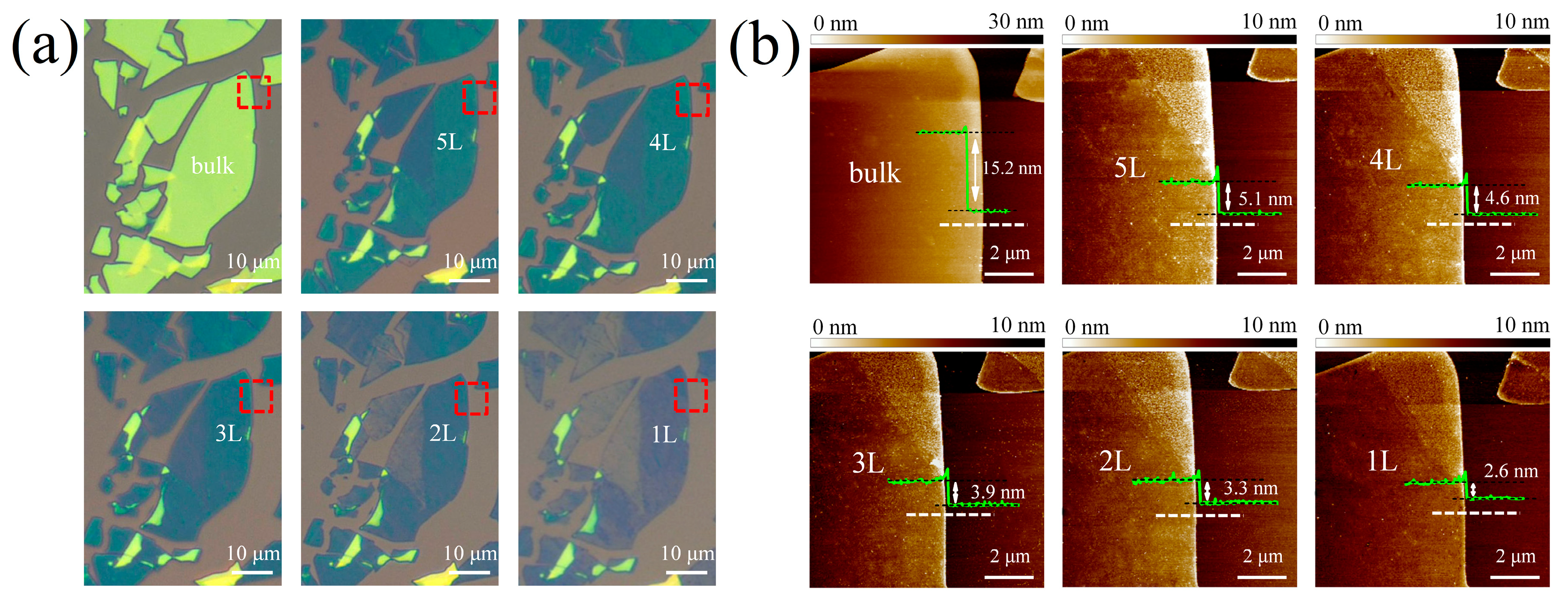
We repeated multiple oxidation/oxidized layer removal cycles to perform a layer-by-layer thinning process in large-area thick MoTe2 flakes (Figure 6a). Obviously, the optical contrast of MoTe2 flakes changed significantly after 24 cycles. One cycle corresponded to one layer removal. Figure 6b shows the AFM images and height profiles of the selected areas in Figure 6a. The relationship between the layer thickness and the layer number is plotted in Figure 1b. Obviously, a linear dependence was also found and the slope was the same as that of pristine MoTe2. This further confirms a precise control of the layer number at the atomic scale by using a cyclical thinning process. The surface roughness of thinned flakes was almost comparable to that of the pristine ones, with only a slight increase from 0.2 to 0.25 nm. However, the thinned layer thickness showed an overall upshift of 1.4 nm. Such a shift may originate from the water molecules trapped between the flakes and the substrate in the wet process [39]. Figure 2 also illustrates comparable Raman spectra between the thinned and pristine MoTe2, and almost the same peak intensity ratio B2g/E2g1.
To study the effect of layer thinning on the electrical characteristics of the MoTe2 layers, a back-gated FET device was fabricated on a 300-nm SiO2/Si substrate. The inset of Figure 7a presents an optical image of a device with seven pristine layers in the channel. The electrical behaviors were investigated while thinning the MoTe2 from seven layers to monolayer by using the cyclical thinning method. Figure 7a shows the evolution of the transfer characteristics with different layer numbers. The source–drain voltage was fixed at 5 V. Before thinning, a typical electron-dominated ambipolar behavior was observed in pristine exfoliated layers, where the on-state current in the n-branch (Ion,n) was one order of magnitude larger than that in the p-branch (Ion,p). This asymmetric conduction behavior was attributed to the unequal SBHs for electrons and holes. This was manifested by the non-linear output characteristics measured at Vg = ±40 V in Figure 7b,c. The vacancies were found to be easily formed in MoTe2 due to the weak bonding energy between Mo and Te atoms [40]. The presence of chalcogen vacancies in TMDCs usually causes the Fermi level to pin near the conduction band [41,42]. Consequently, the electron SBH is lower than that of the holes, thus facilitating the electron injection. Due to a smaller bandgap in the thick pristine MoTe2, the current on/off ratio (Ion/off) over the applied gate voltage range was quite small, 2.1 × 10⁴ for n-branch and 3.9 × 10² for p-branch. After cyclical process of O3 oxidation and subsequent oxide removal, Ion,n was found to be significantly suppressed, as exhibited in Figure 7b and it reduced with decreasing layer number (Figure 7a). Meanwhile Ion,p was drastically increased by one order of magnitude after the first cycle (Figure 7d), that is, in the thinned 6L MoTe2, and then gradually declined with decreasing thickness. Simultaneously, Ion,p became more linear in the output characteristics, which means a reduced hole SBH formed after the thinning process. A remarkable increase of Ion/off in the p-type regime (Ion/off,p) was observed with decreasing layer number. This was mainly attributed to the suppression of off-state current from electron conduction. These distinct transport properties between the pristine and O3 treated MoTe2 were possibly caused by the residues of overlying oxide after KOH immersion. The above XPS analysis reveals that MoO3 and TeO2 contributed to p-doping on the underlying MoTe2 layers. The hole carriers residing between the MoTe2 and contact can unpin the Fermi level and lower it toward the valence band edge [38]. Hence, the reduced hole SBH, along with the raised electron SBH made a transition of the dominant role from electron to hole in the ambipolar MoTe2 FET. Meanwhile, as shown in Figure 7a, the oxide doping also shifted the voltage of the charge neutral point towards the positive direction with thinning of the MoTe2 layers. After the first thinning cycle, Ion,p exhibited a decline with decreasing layer number in Figure 7d, which is consistent with previous observations on MoS2 and black phosphorus [43,44]. The conduction paths along the upper layers were eliminated when these layers were removed during the thinning process. An additional access resistance was hence introduced between the electrode and the underlying MoTe2 due to the large interlayer resistance. This access resistance increased as the layers were thinned. Besides, another effect may exist—thinner flakes are more susceptible to Coulomb scattering from the doping species, which leads to a reduction of carrier mobility [45].
4. Conclusions
In summary, we demonstrated a controllable layer thinning of MoTe2 flakes with O3 treatment. Our in-situ Raman investigation revealed that the formed oxide layer on the surface of MoTe2 led to a self-limiting process. This process could be repeated by removal of the oxidized surface to achieve precise layer-by-layer thinning. The thinned MoTe2 flakes showed a comparable optical quality and surface roughness to the pristine exfoliated ones. This thinning process was also accompanied by a p-type doping in the MoTe2 flakes due to oxide layer coverage. The device transfer characteristics of the MoTe2 FET exhibited a conversion from electron-dominated to hole-dominated ambipolar behavior as the thinning cycle increased. The Ion/off was thus significantly increased at the p-branch. It is believed that our cyclical thinning technique can be applicable to other TMDCs, and provides excellent control in preparing TMDC sheets with well-defined thickness.
Author Contributions
Z.-J.Q. and C.C. conceived and designed the experiments; Q.W., J.C., and Y.Z. performed the experiments; L.H. and R.L. analyzed the data; Q.W. wrote the paper; C.C. and Z.-J.Q. revised the manuscript. All authors discussed the results and commented on the manuscript.
Funding
This work is supported partially by National Natural Science Foundation of China (No. 61774042, 61774040), Shanghai Municipal Natural Science Foundation (No. 16ZR1402500, 17ZR1446500, 17ZR1446600), National Young 1000 Talent Plan of China, "First-Class Construction" project of Fudan University (No. XM03170477).
Conflicts of Interest
The authors declare no conflict of interest.
References
- Manzeli, S.; Ovchinnikov, D.; Pasquier, D.; Yazyev, O.V.; Kis, A. 2D Transition Metal Dichalcogenides. Nat. Rev. Mater. 2017, 2, 17033. [Google Scholar] [CrossRef]
- Wang, Q.H.; Kalantar-Zadeh, K.; Kis, A.; Coleman, J.N.; Strano, M.S. Electronics and Optoelectronics of Two-Dimensional Transition Metal Dichalcogenides. Nat. Nanotechnol. 2012, 7, 699–712. [Google Scholar] [CrossRef] [PubMed]
- Mak, K.F.; Shan, J. Photonics and Optoelectronics of 2D Semiconductor Transition Metal Dichalcogenides. Nat. Photonics. 2016, 10, 216–226. [Google Scholar] [CrossRef]
- Mak, K.F.; Lee, C.; Hone, J.; Shan, J.; Heinz, T.F. Atomically Thin MoS2: A New Direct-Gap Semiconductor. Phys. Rev. Lett. 2010, 105, 136805. [Google Scholar] [CrossRef] [PubMed]
- Zhang, Y.; Chang, T.-R.; Zhou, B.; Cui, Y.-T.; Yan, H.; Liu, Z.; Schmitt, F.; Lee, J.; Moore, R.; Chen, Y.; et al. Direct Observation of the Transition from Indirect to Direct Bandgap in Atomically Thin Epitaxial MoSe2. Nat. Nanotechnol. 2014, 9, 111–115. [Google Scholar] [CrossRef]
- Zhao, W.; Ghorannevis, Z.; Chu, L.; Toh, M.; Kloc, C.; Tan, P.-H.; Eda, G. Evolution of Electronic Structure in Atomically Thin Sheets of WS2 and WSe2. ACS Nano 2013, 7, 791–797. [Google Scholar] [CrossRef]
- Di Bartolomeo, A.; Grillo, A.; Urban, F.; Iemmo, L.; Giubileo, F.; Luongo, G.; Amato, G.; Croin, L.; Sun, L.; Liang, S.J.; et al. Asymmetric schottky contacts in bilayer MoS2 field effect transistors. Adv. Funct. Mater. 2018, 28, 1800657. [Google Scholar] [CrossRef]
- Urban, F.; Martucciello, N.; Peters, L.; McEvoy, N.; Di Bartolomeo, A. Environmental effects on the electrical characteristics of back-gated WSe2 field-effect transistors. Nanomaterials 2018, 8, 901. [Google Scholar] [CrossRef]
- Di Bartolomeo, A.; Urban, F.; Passacantando, M.; McEvoy, N.; Peters, L.; Iemmo, L.; Luongo, G.; Romeo, F.; Giubileo, F. A WSe2 vertical field emission transistor. Nanoscale 2019, 11, 1538–1548. [Google Scholar] [CrossRef]
- Ruppert, C.; Aslan, O.B.; Heinz, T.F. Optical Properties and Band Gap of Single- and Few-Layer MoTe2 Crystals. Nano Lett. 2014, 14, 6231–6236. [Google Scholar] [CrossRef]
- Ding, Y.; Wang, Y.; Ni, J.; Shi, L.; Shi, S.; Tang, W. FirstPrinciples Study of Structural, Vibrational and Electronic Properties of Graphene-like MX2 (M = Mo, Nb, W, Ta; X = S, Se, Te) Monolayers. Physica B 2011, 406, 2254–2260. [Google Scholar] [CrossRef]
- Lezama, I.G.; Arora, A.; Ubaldini, A.; Barreteau, C.; Giannini, E.; Potemski, M.; Morpurgo, A.F. Indirect-to-Direct Band Gap Crossover in Few-Layer MoTe2. Nano Lett. 2015, 15, 2336–2342. [Google Scholar] [CrossRef]
- Nakaharai, S.; Yamamoto, M.; Ueno, K.; Tsukagoshi, K. Carrier Polarity Control in α-MoTe2 Schottky Junctions Based on Weak Fermi-Level Pinning. ACS Appl. Mater. Interfaces 2016, 8, 14732–14739. [Google Scholar] [CrossRef]
- Pradhan, N.R.; Rhodes, D.; Feng, S.; Xin, Y.; Memaran, S.; Moon, B.-H.; Terrones, H.; Terrones, M.; Balicas, L. Field-Effect Transistors Based on Few-Layered α-MoTe2. ACS Nano 2014, 8, 5911–5920. [Google Scholar] [CrossRef]
- Luo, W.; Zhu, M.; Peng, G.; Zheng, X.; Miao, F.; Bai, S.; Zhang, A.; Qin, S. Carrier Modulation of Ambipolar Few-Layer MoTe2 Transistors by MgO Surface Charge Transfer Doping. Adv. Funct. Mater. 2018, 28, 1704539. [Google Scholar] [CrossRef]
- Nakaharai, S.; Yamamoto, M.; Ueno, K.; Lin, Y.-F.; Li, S.-L.; Tsukagoshi, K. Electrostatically Reversible Polarity of Ambipolar α-MoTe2 Transistors. ACS Nano 2015, 9, 5976–5983. [Google Scholar] [CrossRef]
- Qu, D.; Liu, X.; Huang, M.; Lee, C.; Ahmed, F.; Kim, H.; Ruoff, S.; Hone, J.; Yoo, J. Carrier-Type Modulation and Mobility Improvement of Thin MoTe2. Adv. Mater. 2017, 29, 1606433. [Google Scholar] [CrossRef]
- Lin, Y.-F.; Xu, Y.; Wang, S.-T.; Li, S.-L.; Yamamoto, M.; Aparecido-Ferreira, A.; Li, W.; Sun, H.; Nakaharai, S.; Jian, W.-B.; et al. Ambipolar MoTe2 Transistors and Their Applications in Logic Circuits. Adv. Mater. 2014, 26, 3263–3269. [Google Scholar] [CrossRef] [PubMed]
- Novoselov, K.S.; Geim, A.K.; Morozov, S.; Jiang, D.; Zhang, Y.; Dubonos, S.V.; Grigorieva, I.V.; Firsov, A.A. Electric Field Effect in Atomically Thin Carbon Films. Science 2004, 306, 666. [Google Scholar] [CrossRef] [PubMed]
- Coleman, J.N.; Lotya, M.; O’Neill, A.; Bergin, S.D.; King, P.J.; Khan, U.; Young, K.; Gaucher, A.; De, S.; Smith, R.J.; et al. Two-Dimensional Nanosheets Produced by Liquid Exfoliation of Layered Materials. Science 2011, 331, 568–571. [Google Scholar] [CrossRef] [Green Version]
- Lee, Y.H.; Zhang, X.Q.; Zhang, W.J.; Chang, M.T.; Lin, C.T.; Chang, K.D.; Yu, Y.C.; Wang, J.T.W.; Chang, C.S.; Li, L.J.; et al. Synthesis of Large-Area MoS2 Atomic Layers with Chemical Vapor Deposition. Adv. Mater. 2012, 24, 2320–2325. [Google Scholar] [CrossRef]
- Castellanos-Gomez, A.; Barkelid, M.; Goossens, A.M.; Calado, V.E.; van der Zant, H.S.J.; Steele, G.A. Laser thinning of MoS2: On demand generation of a single-layer semiconductor. Nano Lett. 2012, 12, 3187–3192. [Google Scholar] [CrossRef]
- Wu, J.; Li, H.; Yin, Z.; Li, H.; Liu, H.; Liu, J.; Cao, X.; Zhang, Q.; Zhang, H. Layer Thinning and Etching of Mechanically Exfoliated MoS2 Nanosheets by Thermal Annealing in Air. Small 2013, 19, 3314–3319. [Google Scholar]
- Liu, Y.; Nan, H.; Wu, X.; Pan, W.; Wang, W.; Bai, J.; Zhao, W.; Sun, L.; Wang, X.; Ni, Z. Layer-by-Layer Thinning of MoS2 by Plasma. ACS Nano 2013, 7, 4202–4209. [Google Scholar] [CrossRef] [PubMed]
- Yamamoto, M.; Dutta, S.; Aikawa, S.; Nakaharai, S.; Wakabayashi, K.; Fuhrer, M.S.; Ueno, K.; Tsukagoshi, K. Self- Limiting Layer-by-Layer Oxidation of Atomically Thin WSe2. Nano Lett. 2015, 15, 2067–2073. [Google Scholar] [CrossRef] [PubMed]
- Kim, S.; Jung, Y.; Lee, J.-Y.; Lee, G.-H.; Kim, J. In situ thickness control of black phosphorus field-effect transistors via ozone treatment. Nano Res. 2016, 9, 3056–3065. [Google Scholar] [CrossRef]
- Su, W.; Kumar, N.; Spencer, S.J.; Dai, N.; Roy, D. Transforming bilayer MoS2 into single-layer with strong photoluminescence using UV-ozone oxidation. Nano Res. 2015, 8, 3878–3886. [Google Scholar] [CrossRef]
- Zheng, X.; Wei, Y.; Deng, C.; Huang, H.; Yu, Y.; Wang, G.; Peng, G.; Zhu, Z.; Zhang, Y.; Jiang, T.; et al. Controlled Layer-by-Layer Oxidation of MoTe2 via O3 Exposure. ACS Appl. Mater. Interfaces 2018, 10, 30045–30050. [Google Scholar] [CrossRef] [PubMed]
- Li, H.; Wu, J.; Huang, X.; Lu, G.; Yang, J.; Lu, X.; Xiong, Q.; Zhang, H. Rapid and Reliable Thickness Identification of Two-Dimensional Nanosheets Using Optical Microscopy. ACS Nano 2013, 7, 10344–10353. [Google Scholar] [CrossRef] [PubMed] [Green Version]
- Puotinen, D.; Newnham, R.E. The Crystal Structure of MoTe2. Acta Crystallogr. 1961, 14, 691–692. [Google Scholar] [CrossRef]
- Gołasa, K.; Grzeszczyk, M.; Molas, M.R.; Zinkiewicz, M.; Bala, Ł.; Nogajewski, K.; Potemski, M.; Wysmołek, A.; Babiński, A. Resonant quenching of Raman scattering due to out-of-plane A1g/A1’ modes in few-layer MoTe2. Nanophotonics 2017, 6, 1281–1288. [Google Scholar] [CrossRef]
- Grzeszczyk, M.; Golasa, K.; Zinkiewicz, M.; Nogajewski, K.; Molas, M.R.; Potemski, M.; Wysmolek, A.; Babinski, A. Raman scattering of few-layers MoTe2. 2D Mater. 2016, 3, 025010. [Google Scholar] [CrossRef]
- Yamamoto, M.; Wang, S.T.; Ni, M.Y.; Lin, Y.F.; Li, S.L.; Aikawa, S.; Jian, W.B.; Ueno, K.; Wakabayashi, K.; Tsukagoshi, K. Strong Enhancement of Raman Scattering from a Bulk-Inactive Vibrational Mode in Few-Layer MoTe2. ACS Nano 2014, 8, 3895–3903. [Google Scholar] [CrossRef]
- Song, Q.J.; Tan, Q.H.; Zhang, X.; Wu, J.B.; Sheng, B.W.; Wan, Y.; Wang, X.Q.; Dai, L.; Tan, P.H. Physical origin of Davydov splitting and resonant Raman spectroscopy of Davydov components in multilayer MoTe2. Phys. Rev. B 2016, 93, 115409. [Google Scholar] [CrossRef]
- Bernède, J.; Amory, C.; Assmann, L.; Spiesser, M. X-Ray Photoelectron Spectroscopy Study of MoTe2 Single Crystals and Thin Films. Appl. Surf. Sci. 2003, 219, 238–248. [Google Scholar] [CrossRef]
- Moulder, J.F.; Chastain, J. Handbook of X-Ray Photoelectron Spectroscopy: A Reference Book of Standard Spectra for Identification and Interpretation of XPS Data; Perkin-Elmer Corporation, Physical Electronics Division: Waltham, MA, USA, 1992. [Google Scholar]
- Zhu, H.; Qin, X.; Cheng, L.; Azcatl, A.; Kim, J.; Wallace, R.M. Remote Plasma Oxidation and Atomic Layer Etching of MoS2. ACS Appl. Mater. Interfaces 2016, 8, 19119–19126. [Google Scholar] [CrossRef]
- Chuang, S.; Battaglia, C.; Azcatl, A.; McDonnell, S.; Kang, J.S.; Yin, X.; Tosun, M.; Kapadia, R.; Fang, H.; Wallace, R.M.; et al. MoS2 P-Type Transistors and Diodes Enabled by High Work Function MoOx Contacts. Nano Lett. 2014, 14, 1337–1342. [Google Scholar] [CrossRef] [PubMed]
- Eda, G.; Yamaguchi, H.; Voiry, D.; Fujita, T.; Chen, M.; Chhowalla, M. Photoluminescence from Chemically Exfoliated MoS2. Nano Lett. 2011, 11, 5111–5116. [Google Scholar] [CrossRef]
- Zhou, L.; Xu, K.; Zubair, A.; Liao, A.D.; Fang, W.; Ouyang, F.; Lee, Y.-H.; Ueno, K.; Saito, R.; Palacios, T.; et al. Large-Area Synthesis of High-Quality Uniform Few-Layer MoTe2. J. Am. Chem. Soc. 2015, 137, 11892–11895. [Google Scholar] [CrossRef]
- Guo, Y.; Liu, D.; Robertson, J. Chalcogen Vacancies in Monolayer Transition Metal Dichalcogenides and Fermi Level Pinning at Contacts. Appl. Phys. Lett. 2015, 106, 173106. [Google Scholar] [CrossRef]
- Di Bartolomeo, A.; Genovese, L.; Giubileo, F.; Iemmo, L.; Luongo, G.; Foller, T.; Schleberger, M. Hysteresis in the transfer characteristics of MoS2 transistors. 2D Mater. 2018, 5, 015014. [Google Scholar] [CrossRef]
- Park, J.W.; Jang, S.K.; Kang, D.H.; Kim, D.S.; Jeon, M.H.; Lee, W.O.; Kim, K.S.; Lee, S.J.; Park, J.-H.; Kim, K.N.; et al. Layer-controlled thinning of black phosphorus by an Ar ion beam. J. Mater. Chem. C 2017, 5, 10888–10893. [Google Scholar] [CrossRef]
- Kim, S.W.; Na, J.H.; Choi, W.L.; Chung, H.-J.; Jhang, S.H. Nonuniform Current Distribution Between Individual Layers of Multilayer MoS2, Experimentally Approached by Using a Laser Thinning Technique. J. Korean Phys. Soc. 2016, 69, 1497–1501. [Google Scholar] [CrossRef]
- Ji, H.; Lee, G.; Joo, M.-K.; Yun, Y.; Yi, H.; Park, J.-H.; Suh, D.; Lim, S.C. Thickness-dependent carrier mobility of ambipolar MoTe2: Interplay between interface trap and coulomb scattering. Appl. Phys. Lett. 2017, 110, 183501. [Google Scholar] [CrossRef]
Figure 1.
(a) Optical images and the corresponding AFM images of monolayer (1L) to pentalayer (5L) pristine MoTe2 flakes on SiO2/Si substrate. The regions enclosed by the red dashed lines indicate the AFM scanned areas. The green curves are AFM height profiles taken along the white dashed lines on the AFM images. (b) Plots of thickness of pristine and thinned MoTe2 versus layer number. Solid lines are linear fits.

Figure 2.
(a) Raman spectra for pristine and thinned MoTe2. All spectra are offset vertically for clarity. (b) The relationship between peak intensity ratio of B2g/E2g1 and the layer number for pristine and thinned MoTe2.
Figure 2.
(a) Raman spectra for pristine and thinned MoTe2. All spectra are offset vertically for clarity. (b) The relationship between peak intensity ratio of B2g/E2g1 and the layer number for pristine and thinned MoTe2.

Figure 3.
Raman spectral evolution of (a) 1L and (c) 2L MoTe2 during O3 exposure. Raman intensities of (b) A1’ and (d) A1g modes as a function of oxidation time.
Figure 3.
Raman spectral evolution of (a) 1L and (c) 2L MoTe2 during O3 exposure. Raman intensities of (b) A1’ and (d) A1g modes as a function of oxidation time.

Figure 4.
(a) AFM images of 2L MoTe2 flake squared in Figure 1a at pristine state (left) and after O3 treatment (right). (b) AFM height profiles of pristine (black line) and oxidized (red line) 2L MoTe2 along the white dashed lines in (a).
Figure 4.
(a) AFM images of 2L MoTe2 flake squared in Figure 1a at pristine state (left) and after O3 treatment (right). (b) AFM height profiles of pristine (black line) and oxidized (red line) 2L MoTe2 along the white dashed lines in (a).

Figure 5.
XPS spectra of (a) Mo 3d and (b) Te 3d core levels of MoTe2 before/after O3 oxidation and after KOH treatment. The black curves are experimental data. The dashed curves are the Lorentzian fits for the peaks of MoTe2, MoO3, and TeO2, respectively. The spectra are offset vertically for clarity.

Figure 6.
(a) Optical images of large-area MoTe2 flakes before and after thinned from bulk to 5L, 4L, 3L, 2L and 1L MoTe2. (b) The corresponding AFM images of the selected square regions in (a), with superimposed height profiles along the dashed lines.
Figure 6.
(a) Optical images of large-area MoTe2 flakes before and after thinned from bulk to 5L, 4L, 3L, 2L and 1L MoTe2. (b) The corresponding AFM images of the selected square regions in (a), with superimposed height profiles along the dashed lines.

Figure 7.
(a) Transfer characteristics of a 7L MoTe2 field effect transistor (FET) before and after layer-by-layer thinning. The inset is an optical image of the as-fabricated device. (b,c) Comparison of the output characteristics in the n- and p-type regimes before and after layer thinning. (d) Ion/off,p (left) and Ion,p extracted at Vg = −60 V in (a) (right) plotted as a function of the number of MoTe2 layers. The dashed line is a guide to the eye.

© 2019 by the authors. Licensee MDPI, Basel, Switzerland. This article is an open access article distributed under the terms and conditions of the Creative Commons Attribution (CC BY) license (http://creativecommons.org/licenses/by/4.0/).
Share and Cite
MDPI and ACS Style
Wang, Q.; Chen, J.; Zhang, Y.; Hu, L.; Liu, R.; Cong, C.; Qiu, Z.-J. Precise Layer Control of MoTe2 by Ozone Treatment. Nanomaterials 2019, 9, 756. https://doi.org/10.3390/nano9050756
AMA Style
Wang Q, Chen J, Zhang Y, Hu L, Liu R, Cong C, Qiu Z-J. Precise Layer Control of MoTe2 by Ozone Treatment. Nanomaterials. 2019; 9(5):756. https://doi.org/10.3390/nano9050756
Chicago/Turabian StyleWang, Qiyuan, Jing Chen, Youwei Zhang, Laigui Hu, Ran Liu, Chunxiao Cong, and Zhi-Jun Qiu. 2019. "Precise Layer Control of MoTe2 by Ozone Treatment" Nanomaterials 9, no. 5: 756. https://doi.org/10.3390/nano9050756
Note that from the first issue of 2016, this journal uses article numbers instead of page numbers. See further details here.