Probing the Growth Improvement of Large-Size High Quality Monolayer MoS2 by APCVD


Abstract
:1. Introduction
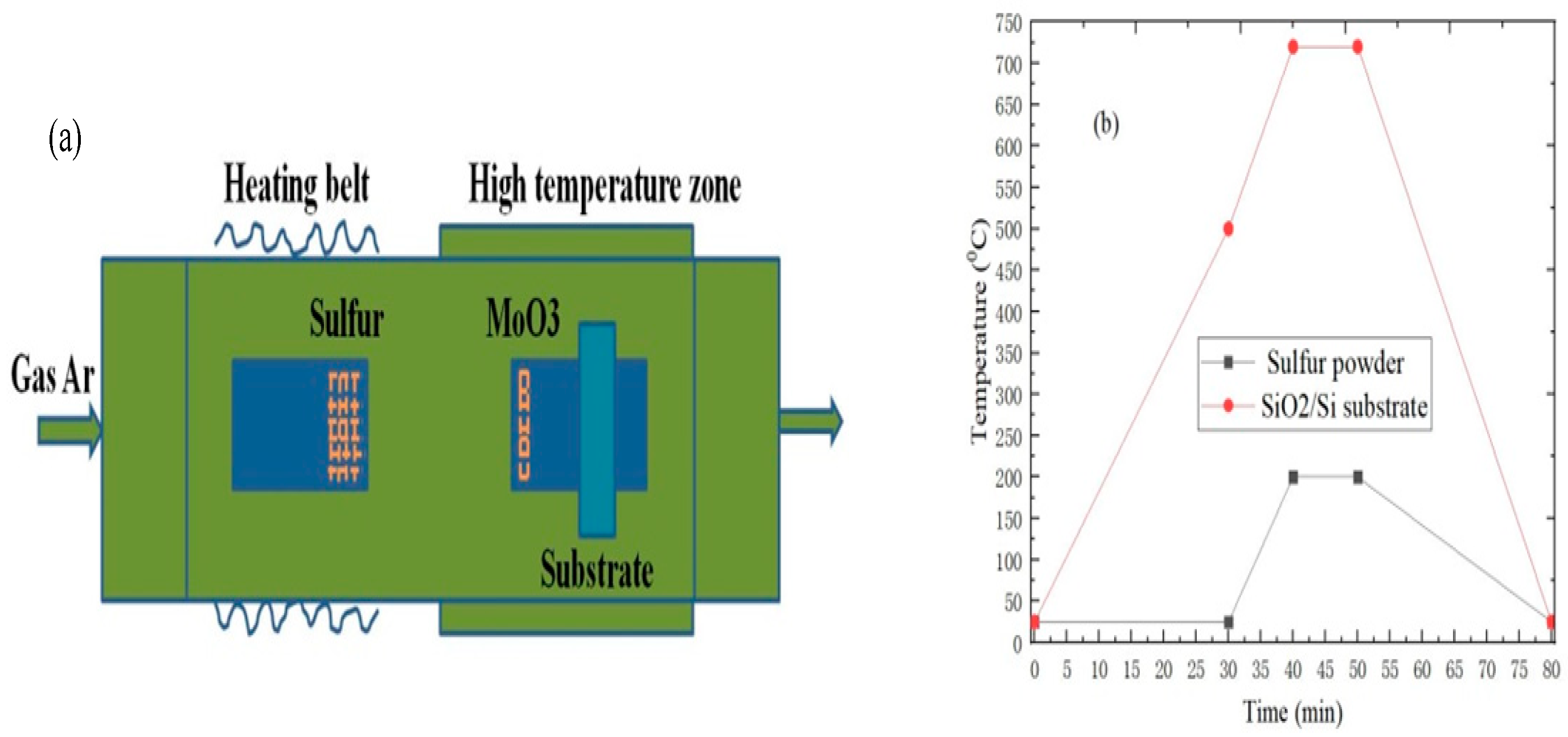
2. Methods
3. Results and Discussion
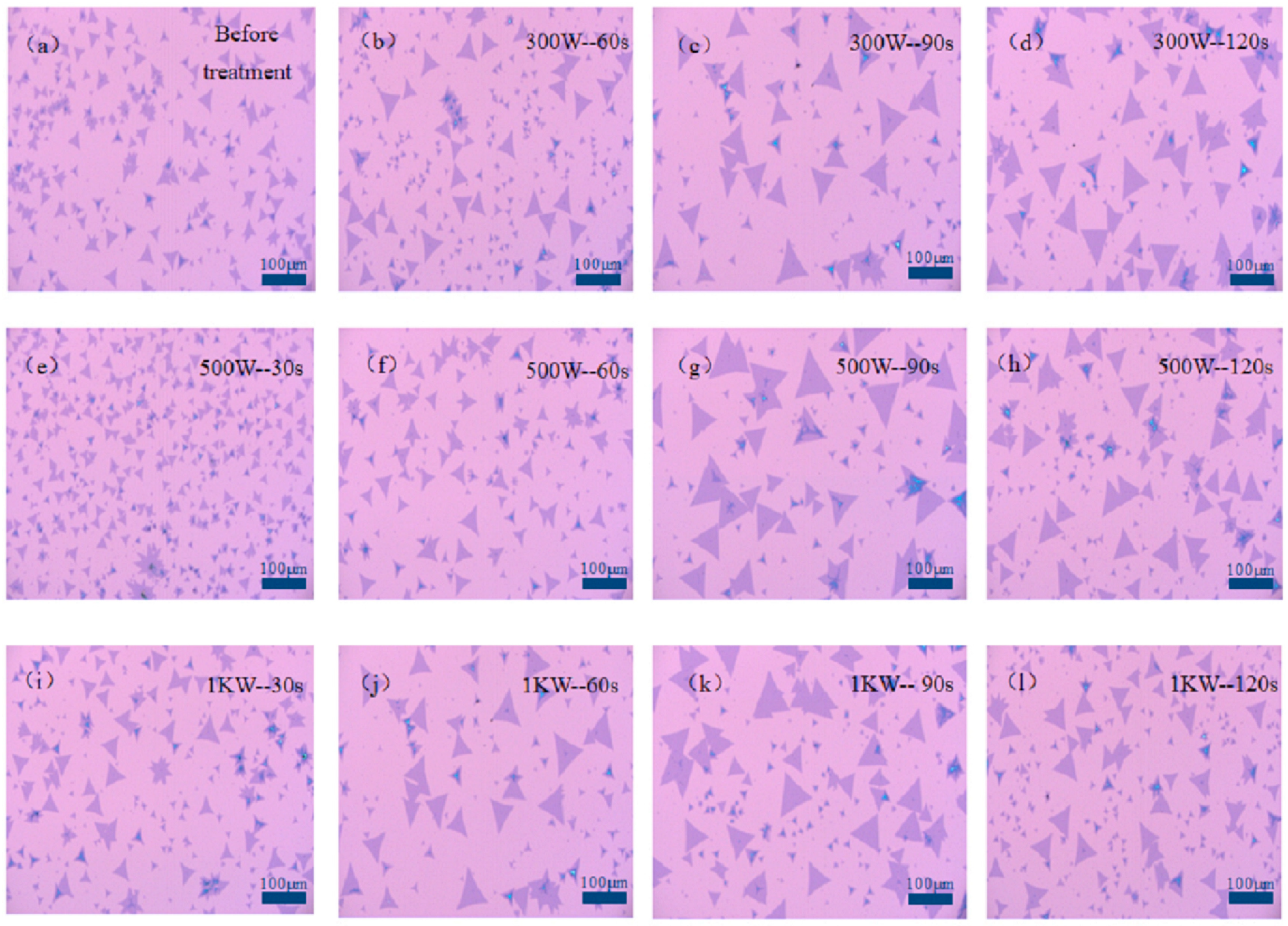
3.1. Effect of Different Oxygen Plasma Treatment Time and Power on the Growth of MoS2
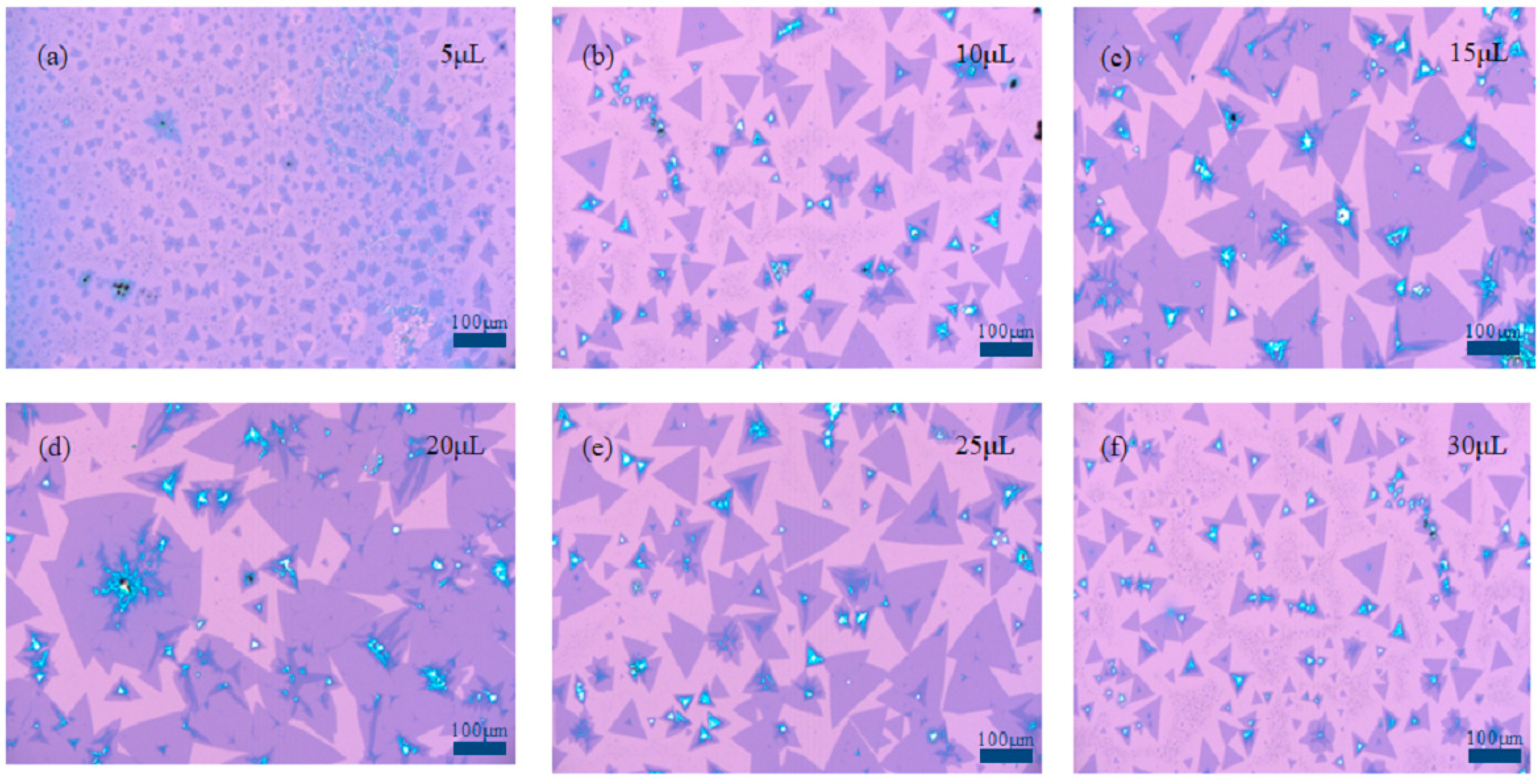
3.2. Effect of Graphene Quantum Dot Solution Amount on the Growth of MoS2
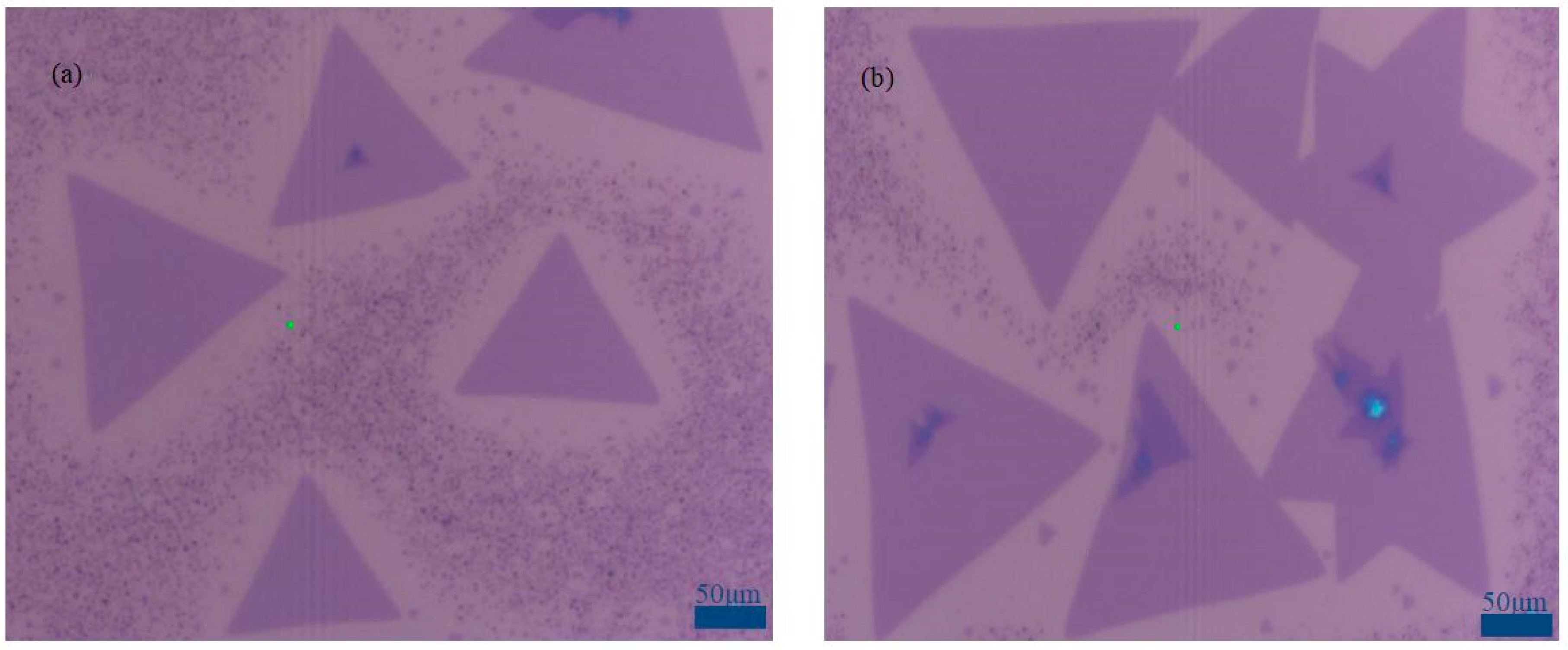
3.3. The Optimal Growth Conditions of Monolayer MoS2
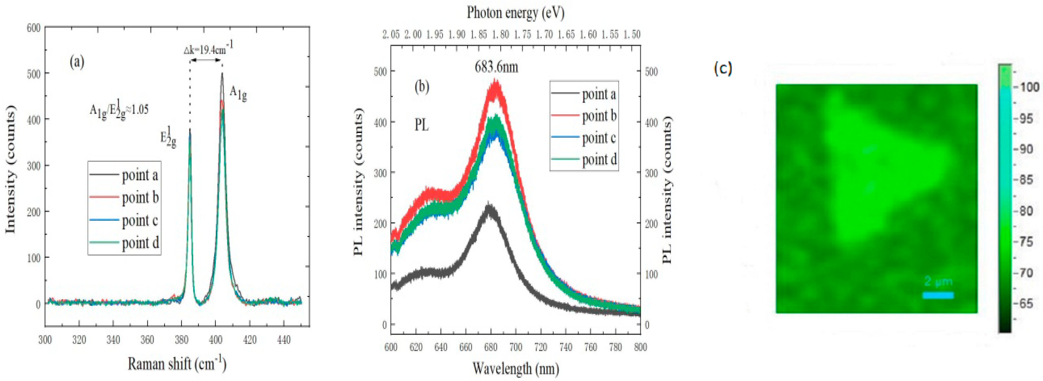
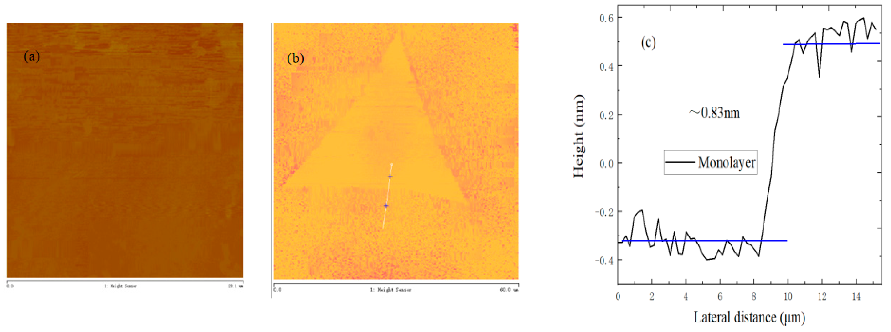
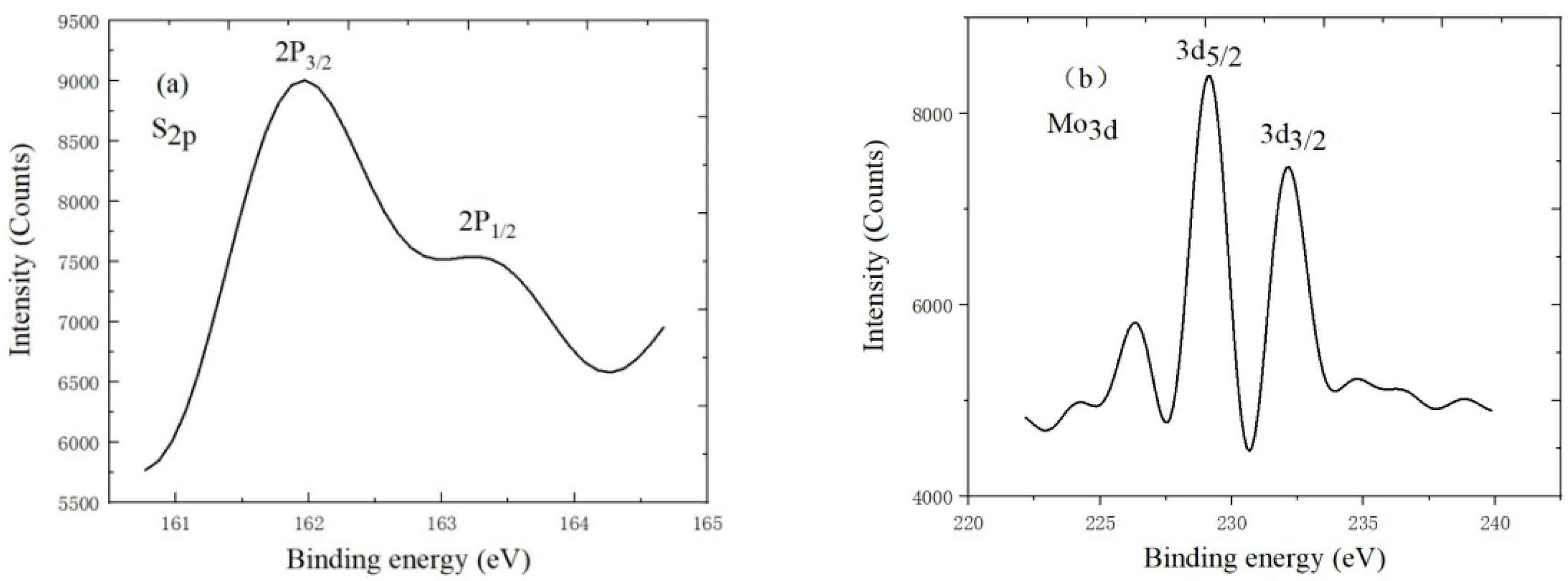
3.4. Characterization of Monolayer MoS2
4. Conclusions
Author Contributions
Funding
Conflicts of Interest
References
- Chae, W.H.; Cain, J.D.; Hanson, E.D.; Murthy, A.A.; Dravid, V.P. Substrate-induced strain and charge doping in CVD-grown monolayer MoS2. Appl. Phys. Lett. 2017, 111, 143106. [Google Scholar] [CrossRef]
- Li, Z.; Li, Y.; Han, T.; Wang, X.; Yu, Y.; Tay, B.; Liu, Z.; Fang, Z. Tailoring MoS2 exciton—Plasmon interaction by optical spin—Orbit coupling. ACS Nano 2016, 11, 1165–1171. [Google Scholar] [CrossRef] [PubMed]
- Momeni, K.; Ji, Y.; Zhang, K.; Robinson, J.A.; Chen, L.-Q. Multiscale framework for simulation-guided growth of 2D materials. Npj 2D Mater. Appl. 2018, 2, 27. [Google Scholar] [CrossRef]
- Xu, H.; Zhou, W.; Zheng, X.; Huang, J.; Feng, X.; Ye, L.; Xu, G.; Lin, F. Control of the nucleation density of molybdenum disulfide in large-scale synthesis using chemical vapor deposition. Materials 2018, 11, 870. [Google Scholar] [CrossRef] [PubMed]
- Das, S.; Chen, H.-Y.; Penumatcha, A.V.; Appenzeller, J. High performance multilayer MoS2 transistors with scandium contacts. Nano Lett. 2013, 13, 100–105. [Google Scholar] [CrossRef] [PubMed]
- Li, D.; Xiao, Z.; Mu, S.; Wang, F.; Liu, Y.; Song, J.; Huang, X.; Jiang, L.; Xiao, J.; Liu, L. A facile space-confined solid-phase sulfurization strategy for growth of high-quality ultrathin molybdenum disulfide single crystals. Nano Lett. 2018, 18, 2021–2032. [Google Scholar] [CrossRef] [PubMed]
- Vilá, R.; Momeni, K.; Wang, Q.; Bersch, B.; Lu, N.; Kim, M.; Chen, L.; Robinson, J. Bottom-up synthesis of vertically oriented two-dimensional materials. 2D Mater. 2016, 3, 041003. [Google Scholar] [CrossRef] [Green Version]
- Zafar, A.; Nan, H.; Zafar, Z.; Wu, Z.; Jiang, J.; You, Y.; Ni, Z. Probing the intrinsic optical quality of CVD grown MoS2. Nano Res. 2017, 10, 1608–1617. [Google Scholar] [CrossRef]
- Zobel, A.; Boson, A.; Wilson, P.M.; Muratov, D.S.; Kuznetsov, D.V.; Sinitskii, A. Chemical vapour deposition and characterization of uniform bilayer and trilayer MoS2 crystals. J. Mater. Chem. C 2016, 4, 11081–11087. [Google Scholar] [CrossRef]
- Bertolazzi, S.; Krasnozhon, D.; Kis, A. Nonvolatile memory cells based on MoS2/graphene heterostructures. ACS Nano 2013, 7, 3246. [Google Scholar] [CrossRef]
- Zhang, F.; Momeni, K.; AlSaud, M.A.; Azizi, A.; Hainey, M.F., Jr.; Redwing, J.M.; Chen, L.-Q.; Alem, N. Controlled synthesis of 2D transition metal dichalcogenides: From vertical to planar MoS2. 2D Mater. 2017, 4, 025029. [Google Scholar] [CrossRef]
- Ning, F.; Wang, D.; Feng, Y.-X.; Tang, L.-M.; Zhang, Y.; Chen, K.-Q. Strong interfacial interaction and enhanced optical absorption in graphene/InAs and MoS2/InAs heterostructures. J. Mater. Chem. C 2017, 5, 9429–9438. [Google Scholar] [CrossRef]
- Sundaram, R.; Engel, M.; Lombardo, A.; Krupke, R.; Ferrari, A.; Avouris, P.; Steiner, M. Electroluminescence in single layer MoS2. Nano Lett. 2013, 13, 1416–1421. [Google Scholar] [CrossRef]
- Jia, G.Y.; Liu, Y.; Gong, J.Y.; Lei, D.Y.; Wang, D.L.; Huang, Z.X. Excitonic quantum confinement modified optical conductivity of monolayer and few-layered MoS2. J. Mater. Chem. C 2016, 4, 8822–8828. [Google Scholar] [CrossRef]
- Novoselov, K.; Jiang, D.; Schedin, F.; Booth, T.; Khotkevich, V.; Morozov, S.; Geim, A. Two-dimensional atomic crystals. Proc. Natl. Acad. Sci. USA 2005, 102, 10451–10453. [Google Scholar] [CrossRef] [Green Version]
- Jiang, L.; Lin, B.; Li, X.; Song, X.; Xia, H.; Li, L.; Zeng, H. Monolayer MoS2–graphene hybrid aerogels with controllable porosity for lithium-ion batteries with high reversible capacity. ACS Appl. Mater. Interfaces 2016, 8, 2680–2687. [Google Scholar] [CrossRef]
- Plechinger, G.; Mann, J.; Preciado, E.; Barroso, D.; Nguyen, A.; Eroms, J.; Schueller, C.; Bartels, L.; Korn, T. A direct comparison of CVD-grown and exfoliated MoS2 using optical spectroscopy. Semicond. Sci. Technol. 2014, 29, 064008. [Google Scholar] [CrossRef]
- Zhang, Y.; Xu, L.; Walker, W.R.; Tittle, C.M.; Backhouse, C.J.; Pope, M.A. Langmuir films and uniform, large area, transparent coatings of chemically exfoliated MoS2 single layers. J. Mater. Chem. C 2017, 5, 11275–11287. [Google Scholar] [CrossRef]
- Wu, J.; Dai, J.; Shao, Y.; Cao, M.; Wu, X. Carbon dot-assisted hydrothermal synthesis of flower-like MoS2 nanospheres constructed by few-layered multiphase MoS2 nanosheets for supercapacitors. RSC Adv. 2016, 6, 77999–78007. [Google Scholar] [CrossRef]
- Fadil, D.; Hossain, R.F.; Saenz, G.A.; Kaul, A.B. On the chemically-assisted excitonic enhancement in environmentally-friendly solution dispersions of two-dimensional MoS2 and WS2. J. Mater. Chem. C 2017, 5, 5323–5333. [Google Scholar] [CrossRef]
- Li, Z.; Ye, R.; Feng, R.; Kang, Y.; Zhu, X.; Tour, J.M.; Fang, Z. Graphene quantum dots doping of MoS2 monolayers. Adv. Mater. 2015, 27, 5235–5240. [Google Scholar] [CrossRef]
- Rukelj, Z.; Štrkalj, A.; Despoja, V. Optical absorption and transmission in a molybdenum disulfide monolayer. Phys. Rev. B 2016, 94, 115428. [Google Scholar] [CrossRef]
- Choudhury, P.; Ravavarapu, L.; Dekle, R.; Chowdhury, S. Modulating Electronic and Optical Properties of Monolayer MoS2 Using Nonbonded Phthalocyanine Molecules. J. Phys. Chem. C 2017, 121, 2959–2967. [Google Scholar] [CrossRef]
- Qiu, D.; Lee, D.U.; Pak, S.W.; Kim, E.K. Structural and optical properties of MoS2 layers grown by successive two-step chemical vapor deposition method. Thin Solid Films 2015, 587, 47–51. [Google Scholar] [CrossRef]
- Late, D.J.; Huang, Y.-K.; Liu, B.; Acharya, J.; Shirodkar, S.N.; Luo, J.J.; Yan, A.; Charles, D.; Waghmare, U.V.; Dravid, V.P.; Rao, C.N.R. Sensing behavior of atomically thin-layered MoS2 transistors. ACS Nano 2013, 7, 4879. [Google Scholar] [CrossRef]
- He, J.; Fernández, C.; Primo, A.; Garcia, H. One-Step Preparation of Large Area Films of Oriented MoS2 Nanoparticles on Multilayer Graphene and Its Electrocatalytic Activity for Hydrogen Evolution. Materials 2018, 11, 168. [Google Scholar]
- Shastry, T.A.; Balla, I.; Bergeron, H.; Amsterdam, S.H.; Marks, T.J.; Hersam, M.C. Mutual photoluminescence quenching and photovoltaic effect in large-area single-layer MoS2–polymer heterojunctions. ACS Nano 2016, 10, 10573–10579. [Google Scholar] [CrossRef]
- Serna, M.I.; Yoo, S.H.; Moreno, S.; Xi, Y.; Oviedo, J.P.; Choi, H.; Alshareef, H.N.; Kim, M.J.; Minary-Jolandan, M.; Quevedo-Lopez, M.A. Large-area deposition of MoS2 by pulsed laser deposition with in situ thickness control. ACS Nano 2016, 10, 6054–6061. [Google Scholar] [CrossRef]
- Yu, F.; Liu, Q.; Gan, X.; Hu, M.; Zhang, T.; Li, C.; Kang, F.; Terrones, M.; Lv, R. Ultrasensitive Pressure Detection of Few—Layer MoS2. Adv. Mater. 2017, 29, 1603266. [Google Scholar] [CrossRef]
- Lopez-Sanchez, O.; Alarcon Llado, E.; Koman, V.; Fontcuberta i Morral, A.; Radenovic, A.; Kis, A. Light generation and harvesting in a van der Waals heterostructure. ACS Nano 2014, 8, 3042–3048. [Google Scholar] [CrossRef]
- Yin, Z.; Li, H.; Li, H.; Jiang, L.; Shi, Y.; Sun, Y.; Lu, G.; Zhang, Q.; Chen, X.; Zhang, H. Single-layer MoS2 phototransistors. ACS Nano 2011, 6, 74–80. [Google Scholar] [CrossRef] [PubMed]


| Growth Method | Characteristics | Size of MoS2 | References |
|---|---|---|---|
| Micromechanical stripping | Simple process, low yield, poor repeatability | 10 µm | [15,16] |
| Lithium ion intercalation | Complicated operation and high cost | 20 µm | [16,17,18] |
| Hydrothermal | Poor crystallization quality | 20~30 µm | [19,20,21] |
| CVD | Layer number cannot control | 30~50 µm | [2,3,4,8,9,10] |
| APCVD | Simple operation, no vacuum treatment | 80~100 µm | [25] |
| APCVD | Oxygen plasma treatment, graphene quantum dot | 200 µm | This paper |
© 2019 by the authors. Licensee MDPI, Basel, Switzerland. This article is an open access article distributed under the terms and conditions of the Creative Commons Attribution (CC BY) license (http://creativecommons.org/licenses/by/4.0/).
Share and Cite
Han, T.; Liu, H.; Wang, S.; Chen, S.; Li, W.; Yang, X. Probing the Growth Improvement of Large-Size High Quality Monolayer MoS2 by APCVD. Nanomaterials 2019, 9, 433. https://doi.org/10.3390/nano9030433
Han T, Liu H, Wang S, Chen S, Li W, Yang X. Probing the Growth Improvement of Large-Size High Quality Monolayer MoS2 by APCVD. Nanomaterials. 2019; 9(3):433. https://doi.org/10.3390/nano9030433
Chicago/Turabian StyleHan, Tao, Hongxia Liu, Shulong Wang, Shupeng Chen, Wei Li, and Xiaoli Yang. 2019. "Probing the Growth Improvement of Large-Size High Quality Monolayer MoS2 by APCVD" Nanomaterials 9, no. 3: 433. https://doi.org/10.3390/nano9030433
APA StyleHan, T., Liu, H., Wang, S., Chen, S., Li, W., & Yang, X. (2019). Probing the Growth Improvement of Large-Size High Quality Monolayer MoS2 by APCVD. Nanomaterials, 9(3), 433. https://doi.org/10.3390/nano9030433