Drain Current Model for Double Gate Tunnel-FETs with InAs/Si Heterojunction and Source-Pocket Architecture

Key Laboratory of Wide Band-Gap Semiconductor technology, School of Microelectronics, Xidian University, Xi’an 710071, China
*
Authors to whom correspondence should be addressed.
Nanomaterials 2019, 9(2), 181; https://doi.org/10.3390/nano9020181
Submission received: 21 December 2018
/
Revised: 12 January 2019
/
Accepted: 28 January 2019
/
Published: 1 February 2019
(This article belongs to the Special Issue Modeling of Complex Interfaces: From Surface Chemistry to Nano Chemistry)
Abstract
:The practical use of tunnel field-effect transistors is retarded by the low on-state current. In this paper, the energy-band engineering of InAs/Si heterojunction and novel device structure of source-pocket concept are combined in a single tunnel field-effect transistor to extensively boost the device performance. The proposed device shows improved tunnel on-state current and subthreshold swing. In addition, analytical potential model for the proposed device is developed and tunneling current is also calculated. Good agreement of the modeled results with numerical simulations verifies the validation of our model. With significantly reduced simulation time while acceptable accuracy, the model would be helpful for the further investigation of TFET-based circuit simulations.
1. Introduction
Owing to the band-to-band tunneling (BTBT) mechanism, Tunnel field-effect transistors (TFETs) allow further scaling of operation voltages, which makes them the most promising alternatives to the conventional metal oxide semiconductor field-effect transistors (MOSFETs) for low-power applications [1,2,3,4]. However, the All-silicon TFET suffers from unacceptably low on-state current, which is even lower than the demand reported by the International Technology Roadmap for Semiconductors (ITRS) [5,6], due to the indirect and large bandgap and thus its practical use is retarded.
To address this issue, various design improvements [7,8,9] and 2D materials [10,11] have been proposed and heterojunction TFET (HTFET) made of Ⅲ-Ⅴ/Si have been studied as promising solution. Among all the Ⅲ-Ⅴ/Si structures, InAs/Si HTFET has been proposed for the highest tunneling current for the p-TFET due to its much lower tunneling mass [12], staggered band lineup and the direct tunneling process [13]. Besides that, with an ultra-thin doping pocket inserted between the heavily doped source and the intrinsic channel region [14,15], the source-pocket TFET (SP-TFET) was proposed for more abrupt tunnel junction and steeper energy band bending, resulting in reduced tunneling distance and improved on-state tunneling current. The energy-band engineering of InAs/Si heterojunction and the novel device structure of SP concept improving the device performance have motivated us to combine both the techniques in a single device to further boost up the characteristics and the InAs/Si HSP-TFET is proposed in this paper. The proposed InAs/Si HSP-TFETs can significantly enhance the device performance.
On the other hand, TFET devices so far are mainly studied by the aid of TCAD simulator, an analytical model which is helpful to provide fast results for circuit simulations is still in ample necessity. Some models [16,17,18] are developed for conventional TFET structures. However, in order to simplify the integration process, the tunneling volume is assumed to be the device volume which is unchanged with the gate voltage. Although the electric field is very large near the source/channel interface, the energy band do not overlap in the region where the distance from the source/channel interface is less than the shortest tunneling distance. Namely, the tunneling window is not open. Thus no BTBT happens. Considering that the BTBT rate changes very rapidly, integrating the BTBT rate over the unchanged device volume sums extremely large but actually non-existent BTBT rate and the current would be overestimated. These models present a brief insight for the design of TFETs, but the simplification is not exactly suitable for the actual physical situation, which would lead to improper results sometimes.
In this paper, we proposed the InAs/Si HSP-TFETs combing InAs/Si heterojunction and the SP technique to improve device performance and study their impact in a single device. Furthermore, an analytical potential model for the proposed device is developed. Based on the potential model, the shortest tunnel distance considering the variation of the tunneling volume with the gate voltage is also presented and the current is calculated by numerically integrating the carrier tunneling rate over the varied tunnel volume. The paper is arranged as follows: Section 2 exhibits the mechanism of the proposed InAs/Si HSP-TFET. The model derivation of this work is shown in Section 3. The results and discussions are shown in Sect 4 and Sect 5 gives the conclusion of this work.
2. Heterojunction Source-Pocket DGTFET
The cross section view of the studied InAs/Si HSP-TFET and the coordinate system adopted in this work are shown in Figure 1. The tunneling junction between the N++ source region and the narrow P+ pocket acts as a carrier source for the channel. The device channel can include two regions, as shown in Figure 1, which are the source pocket region denoted as R1 and the rest of channel denoted as R2. Typical values of the device and material parameters used are listed in Table A1 and Table A2 if not otherwise stated.
The effect of the staggered bandgap of InAs/Si heterojunction and the thin fully depleted pocket reduce the tunneling distance and result in more efficient carrier injection from the source region to the channel body. Figure 2 shows the comparison in terms of transfer characteristics, on-state current and average subthreshold swing (SS). The on-state current is extracted at |VGS-Vtunnel| = 1 V, where VGS is the gate-to-source voltage, and Vtunnel is the gate voltage at which the drain current starts to be higher than the reverse leakage current [19]. The average SS is evaluated between Vtunnel and |VGS- Vtunnel| = 1 V. It is shown that the All-Si TFET has an extremely low off-state current (<0.5 fA/μm), but its on-state current is less than 0.5 pA/μm at VGS of 2 V. By applying the staggered bandgap of InAs/Si heterojunction, extraordinary device improvement about a 14000-fold can be obtained in the on-state current with much smaller average SS for the InAs/Si HTFET, compared with the All-Si TFET counterpart. Moreover, by the aid of the heavily doped pocket, the drain current of the HSP-TFET can be further improved by 2.2 times higher than that of the HTFET without SP. It should be pointed out that despite of HSP-TFET simultaneously increased off-state current, it is still much smaller than that of a state-of-the-art 65-nm CMOS transistor which is about 10−11 A/μm [20].
Figure 3 shows the simulated band diagram of InAs/Si HSP-TFET compared with InAs/Si HTFET and All-Si TFET counterparts. The energy band of All-Si TFET has been moved up-forward for the band alignment in drain region with that of InAs/Si HSP-TFET. The large negative gate voltage drop results in an overlap between the channel valence band and the source conductance band. Thus, carriers in the interval of channel valence band edge and source conductance band edge, namely the tunnel window Δφ, can be tunneled from the source conductance band to the channel valence band. As only the carriers in Δφ can tunnel from the source into the channel, the carrier energy distribution is limited and the high energy carriers are effectively filtered. Thus the electronic system is much more immune to the hot carriers compared with a conventional MOSFET [18].
The shortest tunnel distance Wt,min between available source conduction band states and channel valence band states must appear nearby the highest electric field and is one of the most significant parameters in Figure 3a. Wt,min determines the lower bound of the tunnel volume. The more smaller Wt,min, the larger the tunnel volume. Owing to the smaller bandgap of InAs and the large conduction band offset at InAs/Si interface, InAs/Si HTFETs shows much smaller Wt,min (3.49 nm) compared with that (11.08 nm) of All-Si TFETs. Thus much higher tunneling rate and larger tunnel volume are obtained for InAs/Si HTFETs, as shown in Figure 3b, which is consistent with the extraordinary improvement of the on-state current. The Wt,min of InAs/Si HTFET can be further reduced from 3.49 nm to 1.98 nm by applying the heavily doped SP structure as plotted in Figure 3a. Figure 3b shows that the InAs/Si HSP-TFET has greatly elevated tunneling rate, especially over the pocket region, compared with InAs/Si HTFETs and this is the reason of the highest tunnel on-state current for the InAs/Si HSP-TFET as shown in Figure 2.
3. Model Derivation for InAs/Si HSP-TFET
3.1. Channel Potential Model
With the assumption of a fully depleted channel in the subthreshold operation domain, the charge density in the channel region is equal to the ionized doping concentration. Thus the 2D Poisson equations can be used to describe the potential distribution across the regions R1 and R2 as Equation (1) [21].
where Φj(x,y) is the overall channel potential and Ni,j is the doping concentration. The subscript j = 1, 2 for regions R1 and R2, respectively.
The parabolic approximation [22,23] of the potential in the direction normal to the channel surface is adopted, so that the channel potential can be described as an analytical Equation (2).
Here the C1,j(x) and C2,j(x) are arbitrary functions of the surface potential φj(x). At the interface between the channel and the oxide, the electric flux must be continuous. In addition, the electric field in the middle position of the channel along the y-direction equals to zero due to the structure symmetry of device.
where Vgs,j = VGS − VFB,j. VFB,j is the gate flat band voltage. With Equation (3), the coefficient C1,j(x) and C2,j(x) can be expressed as functions of the surface potential φj(x).
By substituting Equation (4), and Equation (2) into Equation (1), the 2D Poisson equations can be reduced to the well-known form.
where β = (2εox/toxtsiεsi)1/2, αj = qNi,j/εsi − β2Vgs,j.
The general solutions for Equation (5) can be expressed as Equation (6).
Undetermined parameters Aj and Bj in Equation (6) can be solved by the boundary conditions, i.e., the potential and electric displacement continuities at the Source/R1, R1/R2 and R2/Drain interfaces.
where ΔVRef = (Eg,Channel − Eg,Source)/2q and ΔEC = χChannel − χSource is the conductance band offset of the InAs/Si heterojunction interface. ni,Source and ni,Drain are the intrinsic carrier density of source and drain regions, respectively. Vt is the thermal voltage. VS and VD are source and drain bias respectively. The Aj and Bj are solved by substituting Equation (7) into Equation (6), and the results are given in Equation (8).
With
where θ1 = exp(β×Lg) and θ2 = exp(β×LP). Φ1(0,0) and Φ2(Lg,0) are surface potential at x = 0 and x = Lg respectively.
With the obtained surface potential φj(x), the overall channel potential Φj(x,y) can be obtained by Equation (2). Differentiating the channel potential, the electric-field distribution in the channel region can be obtained.
where E(x,y) is the magnitude of the electric field. Ex and Ey are electric field along the x and y directions, respectively. The energy bands are derived from the potential expression Equation (11).
3.2. Drain Current Model
The Wt,min can be used to determine the tunnel volume and calculate the device tunneling current. The carrier tunnel into the channel as the source conduction band and the channel valence band are in-line to each other. Hence, the Wt,min can be obtained as EC,Source = EV,j(Wt,min,y).
With
The Wt,min reduction caused by the increased gate bias boosts the tunneling current due to the larger tunneling volume. Instead of a full quantum treatment, the tunneling carriers are modeled by a generation-recombination process. For a given tunneling path of length L which starts at x = 0 and ends at x = L, holes are generated at x = 0 and electrons are generated at x = L [24]. Thus, the carrier tunneling rate can be equivalently processed by the generation rate and the tunnel current density of carriers tunneling from the source to the channel equals to electron charge times the integral of the generation rate GBTBT. Then the tunnel current can be computed by integrating the tunnel current density over tunnel volume.
Considering the exponential decrease of the tunneling rate with the tunnel distance [25], the BTBT process from source to channel is assumed to be extended up to the channel center and the BTBT process from channel to drain usually known as the ambipolar effect [26] is limited in the right part of the channel. Thus the tunnel current can be described by Equation (14).
The well-known Kane’s Model [27] is used to calculate the generation rate as Equation (15).
In Equation (15), E0 = 1 V/cm and |E| is the electric field magnitude given by Equation (10). The AK and BK are the Kane’s tunneling parameters.
4. Results and Discussion
In this part, the numerical simulations by ISE TCAD tool from Synopsys were carried out to verify the validity of our model. In this work, a non-local path BTBT model along with SRH recombination and bandgap narrowing has been employed for carrier transport.
4.1. Channel Potential
Calculating with the proposed model, the channel surface potential and electric field versus gate voltage along the x-direction are plotted in Figure 4, in which the comparison with the results simulated by TCAD tool are also shown in this figure, and the excellent agreement demonstrates the validation of our model. Owing to the non-uniform modulation of the gate voltage on the channel potential, the potential near the tunneling junction becomes steeper with the increased gate voltage, leading to much larger electric field, which can be seen in Figure 4b. Furthermore, the potential change with the increased gate voltage greatly narrows the tunneling distance for the charge carriers, thus resulting in elevating tunnel probability.
The surface potential distributions of InAs/Si HSP-TFET with different SP doping concentrations are plotted in Figure 5a. Increasing the SP doping concentration results in much more steeper surface potential distribution close to the source end and thus leads to improved electric field and higher drain tunnel current. But the carrier would be injected by diffusion over the barrier with a too heavily doped pocket structure. Thus, the SP doping concentration is fixed at 1 × 1019 cm−3 to guarantee that the carrier transport based on BTBT mechanism. Another critical parameter for the device design is the pocket length and Figure 5b shows the variation of the surface potential with pocket lengths. It can be seen that longer length is helpful to increase the steepness of the potential profile near the source end and therefore will lead to improved on-state tunnel current. The pocket length should be carefully designed because the pocket region with a fixed pocket doping density no longer remains fully depleted if it is too long and in this case, the subthreshold characteristics would be drastically degraded.
Excellent agreement of modeled potential results with the TCAD simulation exhibited in Figure 5 reveals that the presented potential model can predict the impact of pocket doping concentration and pocket length on the potential distribution with good accuracy. It should be noted that although the model is derived for the proposed InAs/Si HSP-TFET, it can also be extended to the homojunction DG-TFET, with correct parameters in Table A2.
4.2. Drain Current
The variation of the shortest tunnel distance with the gate voltage is illustrated in Figure 6. The TCAD simulation results have been extracted by measuring the alignment points between the source conductance band and the channel valence band, and are very sensitive to the meshing strategy. In our simulation, a very fine mesh grid across the tunneling junction is used. The good agreement obtained between the modeled results and the numerical simulations validates the proposed model. It is evident that the tunnel path is reduced significantly as the gate voltage increases. Due to larger tunneling volume and improved electric field, the reduction of Wt,min with gate voltage improves tunneling current.
The pocket length equal to zero in Figure 6 corresponds to the case of HTFET without SP structure. The HSP-TFET with SP structure shows smaller shortest tunneling distance over a large gate-to-source voltage range in the positive tunneling widow, compared with that of HTFET and leads to higher tunnel on-state current. However, in the off-state, corresponding to the region of negative tunneling window indicated by shading, the HSP-TFET exhibits the same tunneling distance with that of HTFET, which predicts almost the same off-state tunnel current.
Figure 7 shows the transfer characteristics calculated from our model for different pocket doping concentrations and pocket lengths. It is obvious that good agreement is obtained between the model results and the numerical simulations in the on-state where the BTBT current dominates. The large deviation in the off-state results from the neglect of the SRH thermal generation which dominates the off-state leakage current. Due to the heavily doped pocket structure, the InAs/Si HSP-TFET exhibits improved drain tunneling current compared with that of InAs/Si HTFETs without SP. This can be understood from Figure 5 in which the HSP-TFET shows a potential minimum near the source-to-channel tunneling junction caused by the inserted SP structure compared with HTFET without SP structure. The reduction of Wt,min and the increase of electric field due to the sharper potential profile help to boost the on-state tunnel current.
The extracted on-state current and average SS, as functions of the source pocket doping and pocket length, are illustrated in Figure 8. Increasing the pocket doping concentration would cause the energy band to change more abruptly near the tunneling junction, as shown in Figure 5. and thus leads to elevated tunneling current and improved average SS. However, different behaviors of the on-state current and average SS versus the pocket length is exhibited in Figure 8b. It shows an optimum pocket length about 6 nm where the on-state current reaches maximum and the average SS reduces to minimum. For a fixed pocket doping, if the pocket length is increased and larger than the optimum value, the pocket no longer remains fully depleted and the mobile carriers in the pocket region screen the gate electric field, which would degrade the on-state current and also the subthreshold swing.
Finally, it is should be noted that although an ideally abrupt and defect/trap-free heterojunction between InAs and Si is assumed in this work to focus on a clear presentation of current model, they are important for the analysis of TFETs. The electrons can be excited from the valence band to the trap states arising from the very high lattice mismatch of about 11.6% between InAs and Si, and subsequent be emitted to the conduction band or vice versa, which leads to increased leakage current of TFETs [13,28]. In addition, this situation can be further degraded by the phonon-assisted tunneling via the trap sates in the bandgap and enhanced recombination process resulted from the traps at or close to the InAs/Si heterojunction [29]. Fortunately, these effects should not significantly affect our discussion, thus, the exclusion is reasonable in the initial stage of the model development. It also should be pointed out that this model is structure-dependent. It can be applied for TFETs made of double gate architecture even inclding other channel materials like germanium, as long as with correct parameters in Table A2.
5. Conclusions
In conclusion, a novel InAs/Si HSP-TFET is proposed to greatly enhance the device performance. The TCAD simulations reveal that the proposed structure shows an on-state current 28000 times higher than that of All-Si TFET and 2.2 times higher than that of InAs/Si HTFET with simultaneously improved subthreshold swing. An analytical potential model with numerically calculated drain current for the InAs/Si HSP-TFET is also developed. The proposed model provides very faster results with acceptable accuracy compared with TCAD simulations and would be helpful to the investigation of TFETs.
Author Contributions
Conceptualization, B.L.; Funding acquisition, Y.Z. (Yuming Zhang); Methodology, H.L.; Project administration, Y.Z. (Yuming Zhang) and Y.Z. (Yimen Zhang); Software, Z.L.; Supervision, H.L.; Validation, Z.L.; Writing—original draft, B.L.; Writing—review & editing, Y.Z. (Yimen Zhang).
Funding
This work was supported by Advance Research Foundation of China (Grant No. 9140Axxx501), National Defense Advance Research project (Grant No. 3151xxxx301) and Frontier innovation program (Grant No. 48xx4).
Conflicts of Interest
The authors declare no conflict of interest.
Appendix A

Table A1.
Device parameters used in the calculation and simulation.
| Quantity | Value |
|---|---|
| Channel length, Lg (nm) | 50 |
| Pocket length, LP (nm) | 6 |
| Source/Drain length, LSD (nm) | 50 |
| Silicon layer thickness, tSi (nm) | 10 |
| Gate dielectric thickness, tox (nm) | 2 |
| Source doping, Ns (cm−3) | 1 × 10²⁰ |
| Pocket doping, NP (cm−3) | 1 × 10¹⁹ |
| Channel doping, Ni (cm−3) | 1 × 10¹⁷ |
| Drain doping, ND (cm−3) | 1 × 10²¹ |
Table A2.
Material parameters used in this work.
| Quantity | Value |
|---|---|
| Vacuum permittivity | ε0 |
| Silicon permittivity, εSi | 11.9ε0 |
| Oxide permittivity, εOX | 3.9ε0 |
| Source Energy band gap (InAs), Eg,Source (eV) | 0.36 |
| Channel Energy band gap (Si), Eg,Channel (eV) | 1.12 |
| Drain Energy band gap (Si), Eg,Drain (eV) | 0.89 |
| Source Affinity, χSource (eV) | 4.93 |
| Channel Affinity, χChannel (eV) | 4.07 |
| Drain Affinity, χDrain (eV) | 4.18 |
| Silicon Conduction density of states, NC,Si (cm−3) | 2.58 × 10¹⁹ |
| Silicon Valance density of states, NV,Si (cm−3) | 1.94 × 10¹⁹ |
| InAs Conduction density of states, NC,InAs (cm−3) | 8.72 × 10¹⁶ |
| InAs Valance density of states, NV,InAs (cm−3) | 6.66 × 10¹⁸ |
References
- Lu, B.; Lu, H.L.; Zhang, Y.; Zhang, Y.; Cui, X.R.; Lv, Z.J.; Liu, C. Fully Analytical Carrier-Based Charge and Capacitance Model for Hetero-Gate-Dielectric Tunneling Field-Effect Transistors. IEEE Trans. Electron Devices 2018, 65, 3555–3561. [Google Scholar] [CrossRef]
- Chen, F.; Ilatikhameneh, H.; Tan, Y.; Gerhard, K.; Rajib, R. Switching Mechanism and the Scalability of vertical-TFETs. IEEE Trans. Electron Devices 2018, 65, 3065–3068. [Google Scholar] [CrossRef]
- Strangio, S.; Palestri, P.; Lan, M. Benchmarks of a III-V TFET technology platform against the 10-nm CMOS FinFET technology node considering basic arithmetic circuits. Solid-State Electron. 2017, 128, 37–42. [Google Scholar] [CrossRef]
- Liu, J.S.; Clavel, M.B.; Hudait, M.K. An Energy-Efficient Tensile-Strained Ge/InGaAs TFET 7T SRAM Cell Architecture for Ultralow-Voltage Applications. IEEE Trans. Electron Devices 2017, 64, 2193–2200. [Google Scholar] [CrossRef]
- Noor, S.L.; Safa, S.; Khan, Z.R. Dual-material double-gate tunnel FET: Gate threshold voltage modeling and extraction. J. Comput. Electron. 2016, 15, 763–769. [Google Scholar] [CrossRef]
- Semiconductor Industry Association (SIA). International Technology Roadmap for Semiconductors 2015. Available online: https://www.semiconductors.org/wp-content/uploads/2018/06/6_2015-ITRS-2.0-Beyond-CMOS.pdf (accessed on 1 February 2019).
- Ameen, T.A.; Ilatikhameneh, H.; Fay, P. Alloy Engineered Nitride Tunneling Field-Effect Transistor: A Solution for the Challenge of Heterojunction TFETs. IEEE Trans. Electron Devices 2018, 66, 736–742. [Google Scholar] [CrossRef]
- Ambika, R.; Keerthana, N.; Srinivasan, R. Realization of Silicon nanotube tunneling FET on junctionless structure using single and multiple gate workfunction. Solid-State Electron. 2017, 127, 45–50. [Google Scholar] [CrossRef]
- Lu, B.; Lu, H.; Zhang, Y.; Zhang, Y.; Lv, Z.; Zhao, Y. A Novel Planar InAs/Si Hetero-TFET with Buried Drain Design and Face-tunneling Technique. In Proceedings of the 2018 14th IEEE International Conference on Solid-State and Integrated Circuit Technology (ICSICT), Qingdao, China, 31 October–3 November 2018. [Google Scholar]
- Giannazzo, F.; Greco, G.; Roccaforte, F.; Sushant, S.S. Vertical transistors based on 2D materials: Status and prospects. Crystals 2018, 8, 70. [Google Scholar] [CrossRef]
- Sarkar, D.; Xie, X.; Liu, W.; Cao, W.; Kang, J.; Gong, Y.; Kraemer, S.; Pulickel, M.A.; Kaustav, B. A subthermionic tunnel field-effect transistor with an atomically thin channel. Nature 2015, 526, 91. [Google Scholar] [CrossRef] [PubMed]
- Mookerjea, S.; Krishnan, R.; Datta, S.; Narayanan, V. Effective capacitance and drive current for tunnel FET (TFET) CV/I estimation. IEEE Trans. Electron Devices 2009, 56, 2092–2098. [Google Scholar] [CrossRef]
- Das, G.D.; Mishra, G.P.; Dash, S. Impact of source-pocket engineering on device performance of dielectric modulated tunnel FET. Superlattices Microstruct. 2018, 124, 131–138. [Google Scholar] [CrossRef]
- Chang, H.Y.; Adams, B.; Chien, P.Y.; Li, J.; Woo, J.C. Improved subthreshold and output characteristics of source-pocket Si tunnel FET by the application of laser annealing. IEEE Trans. Electron Devices 2013, 60, 92–96. [Google Scholar] [CrossRef]
- Mahajan, A.; Dash, D.K.; Banerjee, P.; Sarkar, S.K. Analytical Modeling of Triple-Metal Hetero-Dielectric DG SON TFET. J. Mater. Eng. Perform. 2018, 27, 2693–2700. [Google Scholar] [CrossRef]
- Wang, P.; Zhuang, Y.; Li, C.; Jiang, Z.; Liu, Y. Drain current model for double-gate tunnel field-effect transistor with hetero-gate-dielectric and source-pocket. Microelectron. Reliab. 2016, 59, 30–36. [Google Scholar] [CrossRef]
- Samuel, T.A.; Balamurugan, N.B. Analytical modeling and simulation of germanium single gate silicon on insulator TFET. J. Semicond. 2014, 35, 034002. [Google Scholar] [CrossRef]
- Xu, W.; Wong, H.; Iwai, H. Analytical model of drain current of cylindrical surrounding gate pnin TFET. Solid-State Electron. 2015, 111, 171–179. [Google Scholar] [CrossRef]
- Ionescu, A.M.; Riel, H. Tunnel field-effect transistors as energy-efficient electronic switches. Nature 2011, 479, 329–337. [Google Scholar] [CrossRef] [PubMed]
- Lu, B.; Lu, H.; Zhang, Y.; Zhang, Y.; Cui, X.; Jin, C.; Liu, C. Improved analytical model of surface potentialwith modifiedboundary conditions for double gate tunnel FETs. Microelectron. Reliab. 2017, 79, 231–238. [Google Scholar]
- Madan, J.; Gupta, R.S.; Chaujar, R. Analytical drain current formulation for gate dielectric engineered dual material gate-gate all around-tunneling field effect transistor. Jpn. J. Appl. Phys. 2015, 54, 094202. [Google Scholar] [CrossRef]
- Meshkin, R.; Ziabari, S.A.S.; Jordehi, A.R. A Novel Analytical Approach to Optimize the Work Functions of Dual-Material Double-Gate Tunneling-FETs. Superlattices Microstruct. 2018, 126, 63–71. [Google Scholar] [CrossRef]
- Sentaurus Device User Guide, version H-2013.03; Synopsys, Inc.: Mountain View, CA, USA, 2013; pp. 400–401.
- Wang, C.; Wu, C.; Wang, J.; Huang, Q.; Huang, R. Analytical current model of tunneling field-effect transistor considering the impacts of both gate and drain voltages on tunneling. Sci. China Inf. Sci. 2015, 58, 1–8. [Google Scholar] [CrossRef]
- Nigam, K.; Pandey, S.; Kondekar, N. A Barrier Controlled Charge Plasma-Based TFET With Gate Engineering for Ambipolar Suppression and RF/Linearity Performance Improvement. IEEE Trans. Electron Devices 2017, 64, 2751–2757. [Google Scholar] [CrossRef]
- Kwon, D.W.; Kim, J.H.; Park, E.; Lee, J.; Park, T.; Lee, R.; Park, G. Reduction method of gate-to-drain capacitance by oxide spacer formation in tunnel field-effect transistor with elevated drain. Jpn. J. Appl. Phys. 2016, 55, 06GG04. [Google Scholar] [CrossRef]
- Bessire, C.D.; Bjoörk, M.T.; Schmid, H.; Andreas, S.; Kathleen, B.R.; Heike, R. Trap-assisted tunneling in Si-InAs nanowire heterojunction tunnel diodes. Nano Lett. 2011, 11, 4195–4199. [Google Scholar] [CrossRef] [PubMed]
- Sant, S.; Moselund, K.; Cutaia, D.; Schmid, H.; Mattias, B.; Heike, R.; Andreas, S. Lateral InAs/Si p-type tunnel FETs integrated on Si—Part 2: Simulation study of the impact of interface traps. IEEE Trans. Electron Devices 2016, 63, 4240–4247. [Google Scholar] [CrossRef]
- Björk, M.T.; Schmid, H.; Bessire, C.D.; Moselund, K.E.; Ghoneim, H.; Karg, S.; Lonscher, E.; Riel, H. Si–InAs heterojunction Esaki tunnel diodes with high current densities. Appl. Phys. Lett. 2010, 97, 163501. [Google Scholar] [CrossRef]
Figure 1.
Schematic cross-sectional view of a p-type HSP-TFET.
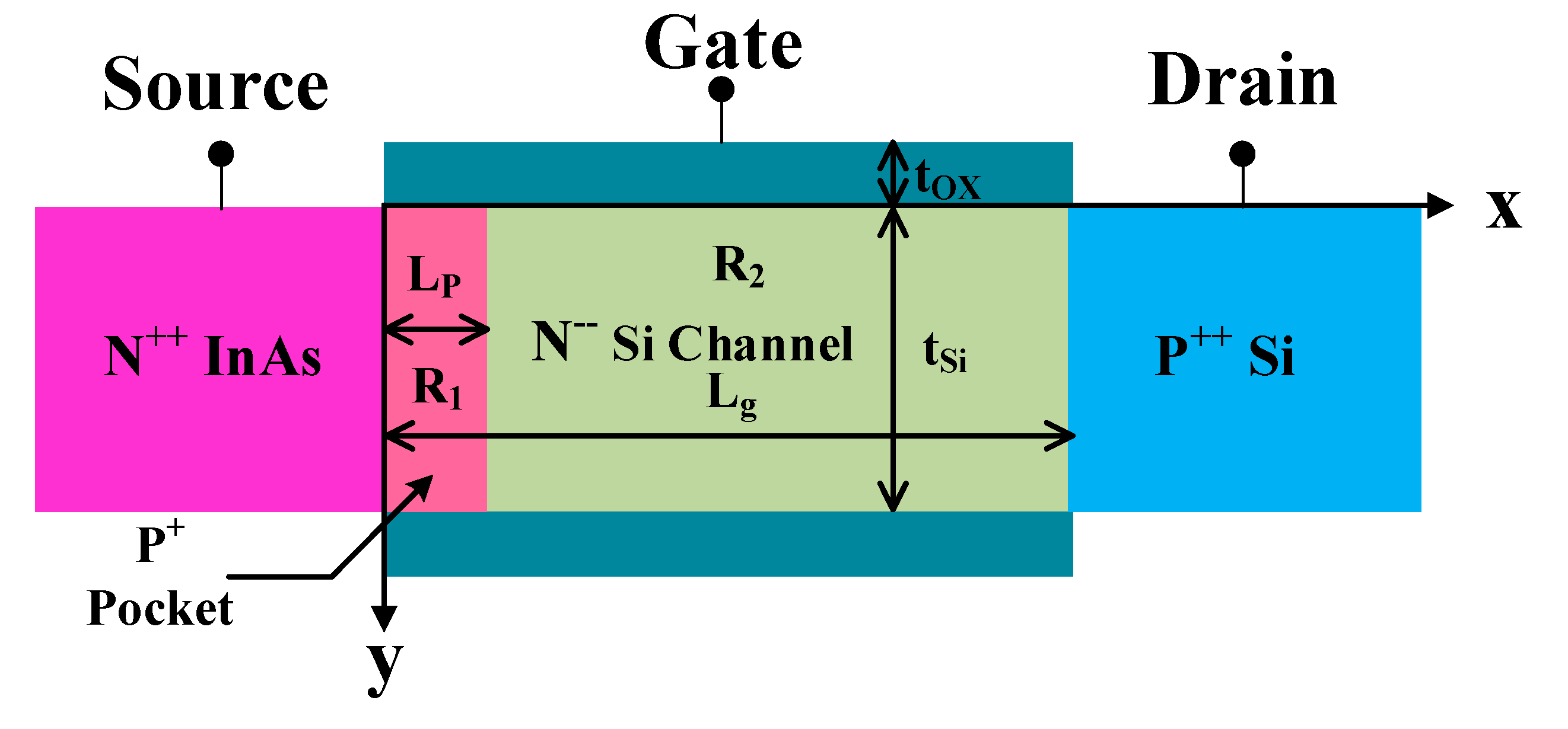
Figure 2.
(a) Simulated ID-VG curves for different TFET configurations. (b) Plots for comparison of the on-state current and SS. The HSP-TFET is with the pocket doping NP = 1 × 1019 cm−3 and the pocket length is LP = 6 nm. The gate work function is 4.3 eV and drain bias is −0.5 V.
Figure 2.
(a) Simulated ID-VG curves for different TFET configurations. (b) Plots for comparison of the on-state current and SS. The HSP-TFET is with the pocket doping NP = 1 × 1019 cm−3 and the pocket length is LP = 6 nm. The gate work function is 4.3 eV and drain bias is −0.5 V.

Figure 3.
(a) Illustration of the energy band diagrams and (b) carrier band to band tunneling rate profile along the channel/oxide interface.
Figure 3.
(a) Illustration of the energy band diagrams and (b) carrier band to band tunneling rate profile along the channel/oxide interface.

Figure 4.
Variation of (a) the surface potential and (b) the lateral electric field with VGS.

Figure 5.
Surface Potential along the channel with (a) the pocket doping concentrations and (b) the pocket lengths.
Figure 5.
Surface Potential along the channel with (a) the pocket doping concentrations and (b) the pocket lengths.

Figure 6.
Shortest tunneling distance versus gate voltage. The pocket doping density for HSP-TFET is 1 × 1019 cm−3. The gate work function is 4.7 eV and the drain bias is 0.5 V.
Figure 6.
Shortest tunneling distance versus gate voltage. The pocket doping density for HSP-TFET is 1 × 1019 cm−3. The gate work function is 4.7 eV and the drain bias is 0.5 V.

Figure 7.
Transfer characteristics versus different (a) pocket doping concentrations and (b) pocket lengths.
Figure 7.
Transfer characteristics versus different (a) pocket doping concentrations and (b) pocket lengths.

Figure 8.
Plot of simulated on-state current and average SS as functions of (a) pocket doping concentration and (b) pocket length. The NP = 1 × 1017 cm−3 and LP = 0 nm correspond to the case of HTFET without SP structure.
Figure 8.
Plot of simulated on-state current and average SS as functions of (a) pocket doping concentration and (b) pocket length. The NP = 1 × 1017 cm−3 and LP = 0 nm correspond to the case of HTFET without SP structure.

© 2019 by the authors. Licensee MDPI, Basel, Switzerland. This article is an open access article distributed under the terms and conditions of the Creative Commons Attribution (CC BY) license (http://creativecommons.org/licenses/by/4.0/).
Share and Cite
MDPI and ACS Style
Lu, H.; Lu, B.; Zhang, Y.; Zhang, Y.; Lv, Z. Drain Current Model for Double Gate Tunnel-FETs with InAs/Si Heterojunction and Source-Pocket Architecture. Nanomaterials 2019, 9, 181. https://doi.org/10.3390/nano9020181
AMA Style
Lu H, Lu B, Zhang Y, Zhang Y, Lv Z. Drain Current Model for Double Gate Tunnel-FETs with InAs/Si Heterojunction and Source-Pocket Architecture. Nanomaterials. 2019; 9(2):181. https://doi.org/10.3390/nano9020181
Chicago/Turabian StyleLu, Hongliang, Bin Lu, Yuming Zhang, Yimen Zhang, and Zhijun Lv. 2019. "Drain Current Model for Double Gate Tunnel-FETs with InAs/Si Heterojunction and Source-Pocket Architecture" Nanomaterials 9, no. 2: 181. https://doi.org/10.3390/nano9020181
Note that from the first issue of 2016, this journal uses article numbers instead of page numbers. See further details here.