Investigation of Position Sensing and Energy Harvesting of a Flexible Triboelectric Touch Pad

 ,
, 

 ,
, 

Abstract
:1. Introduction
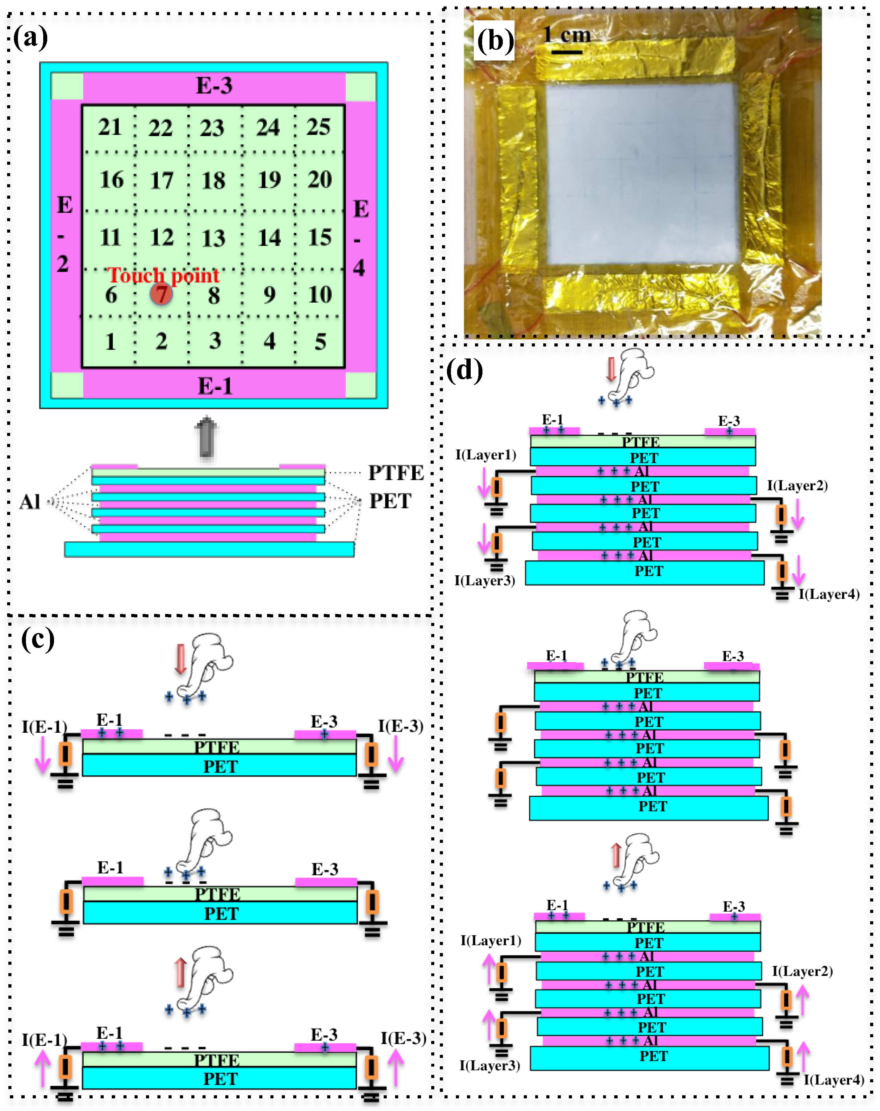
2. Materials and Device Configuration
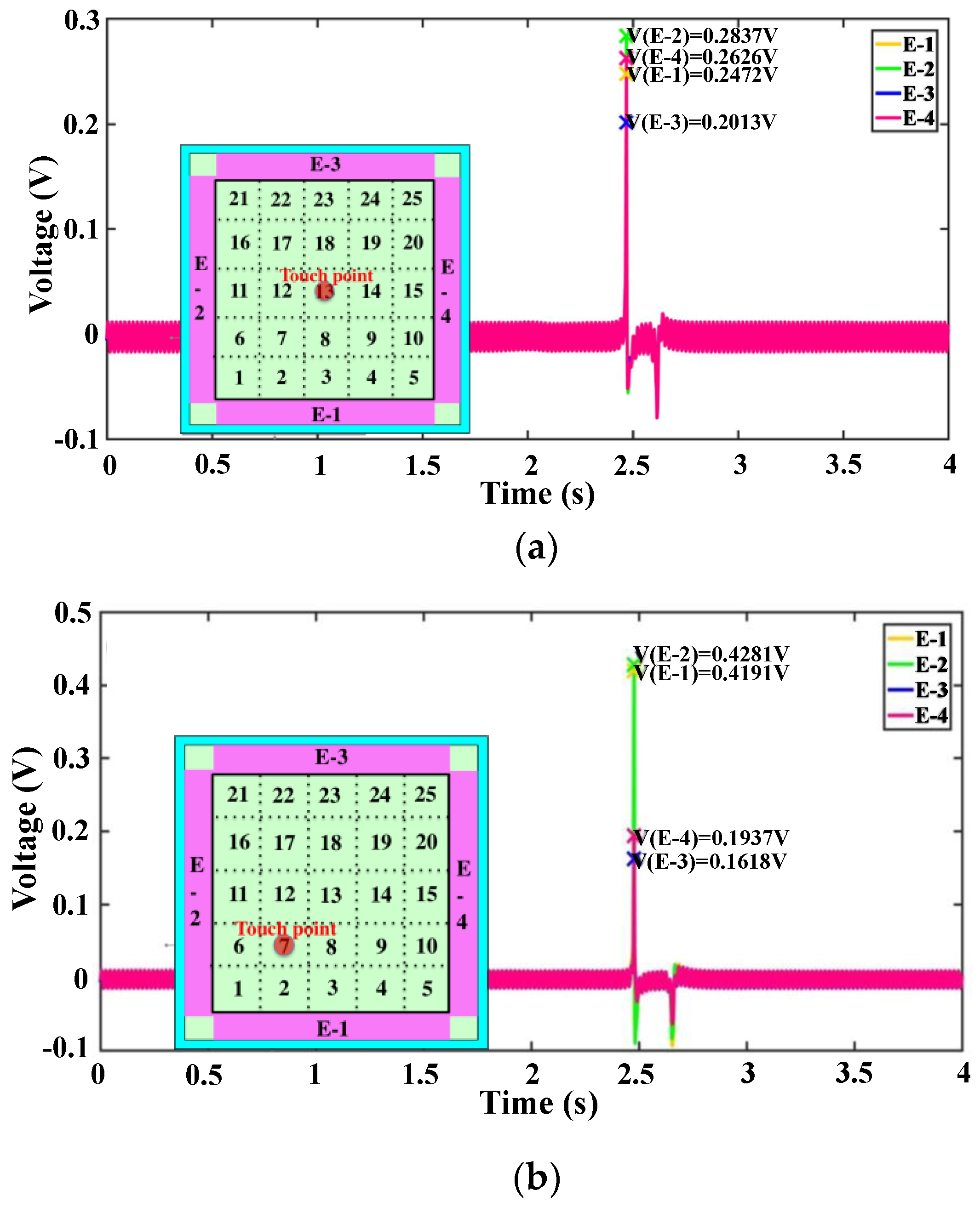
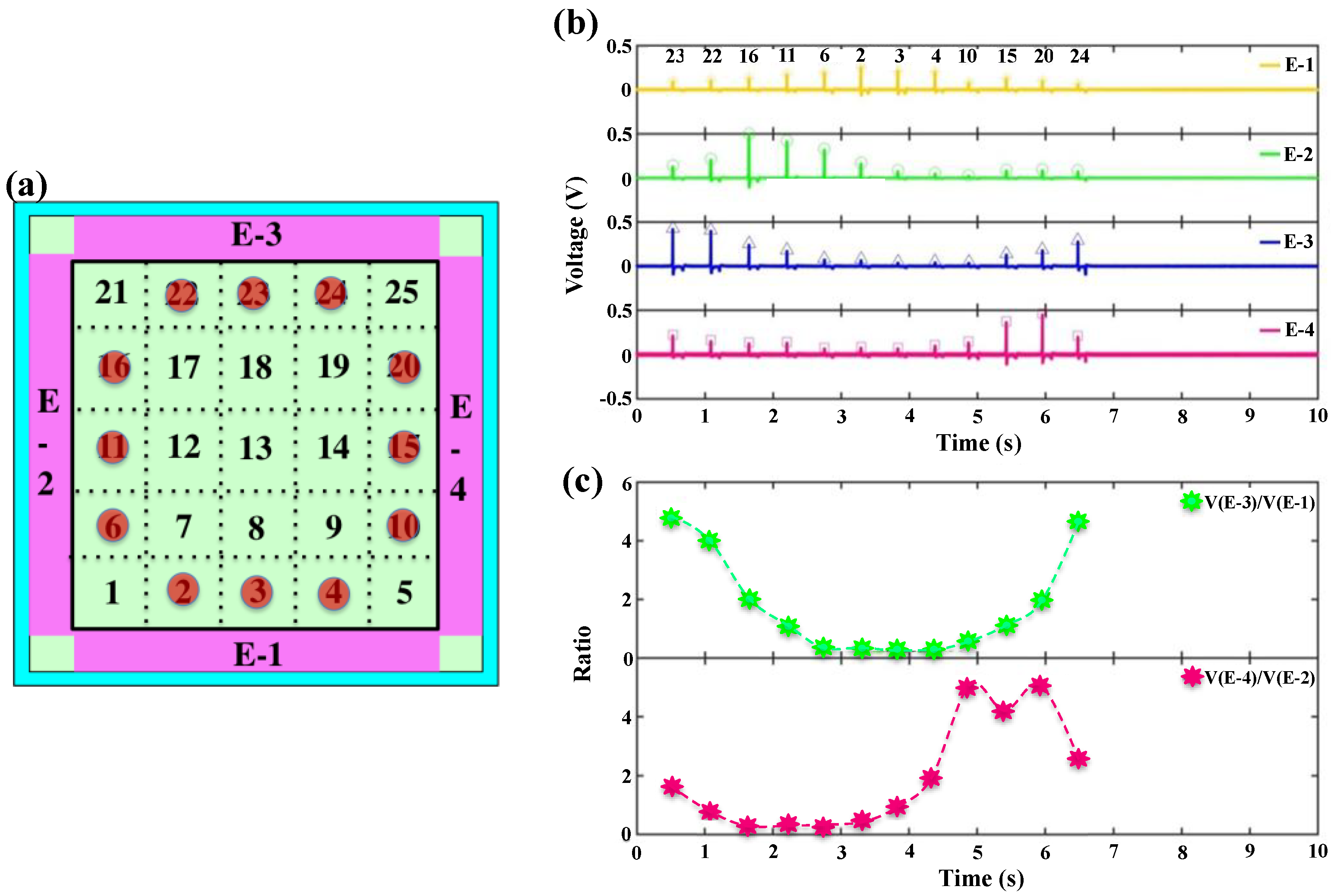
3. Characterization of Position Sensing
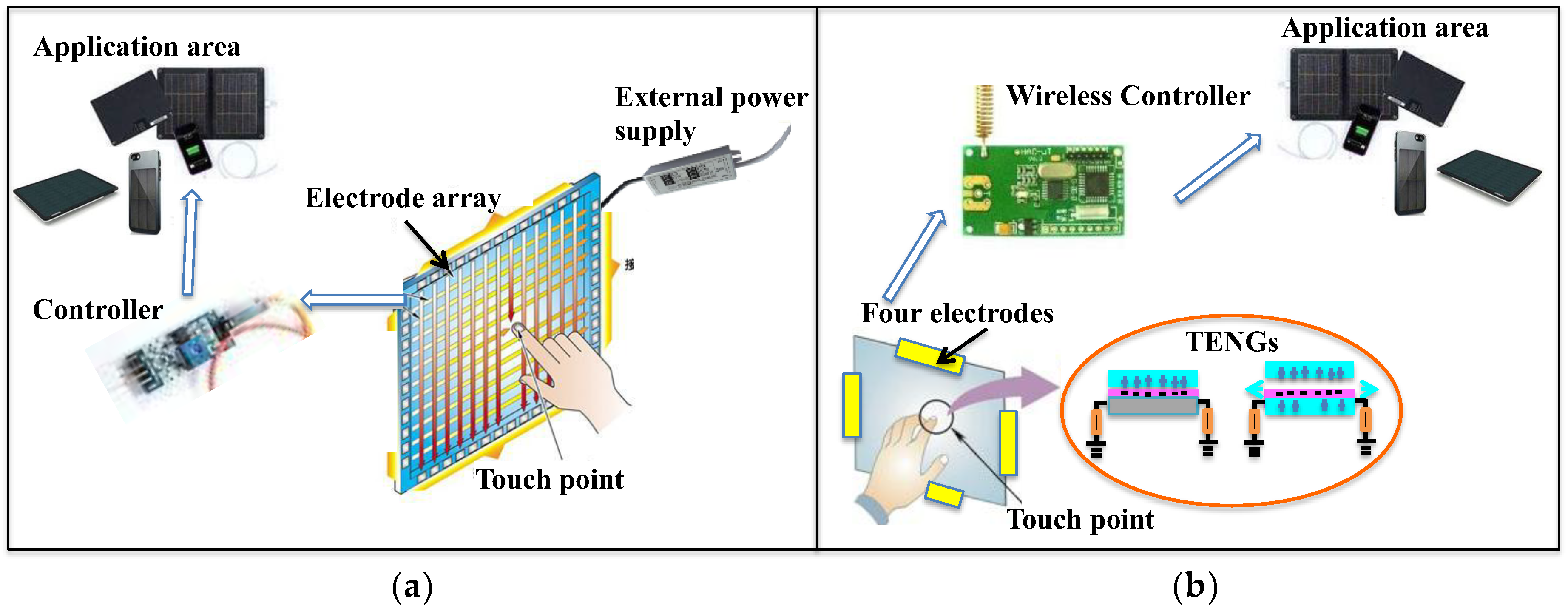
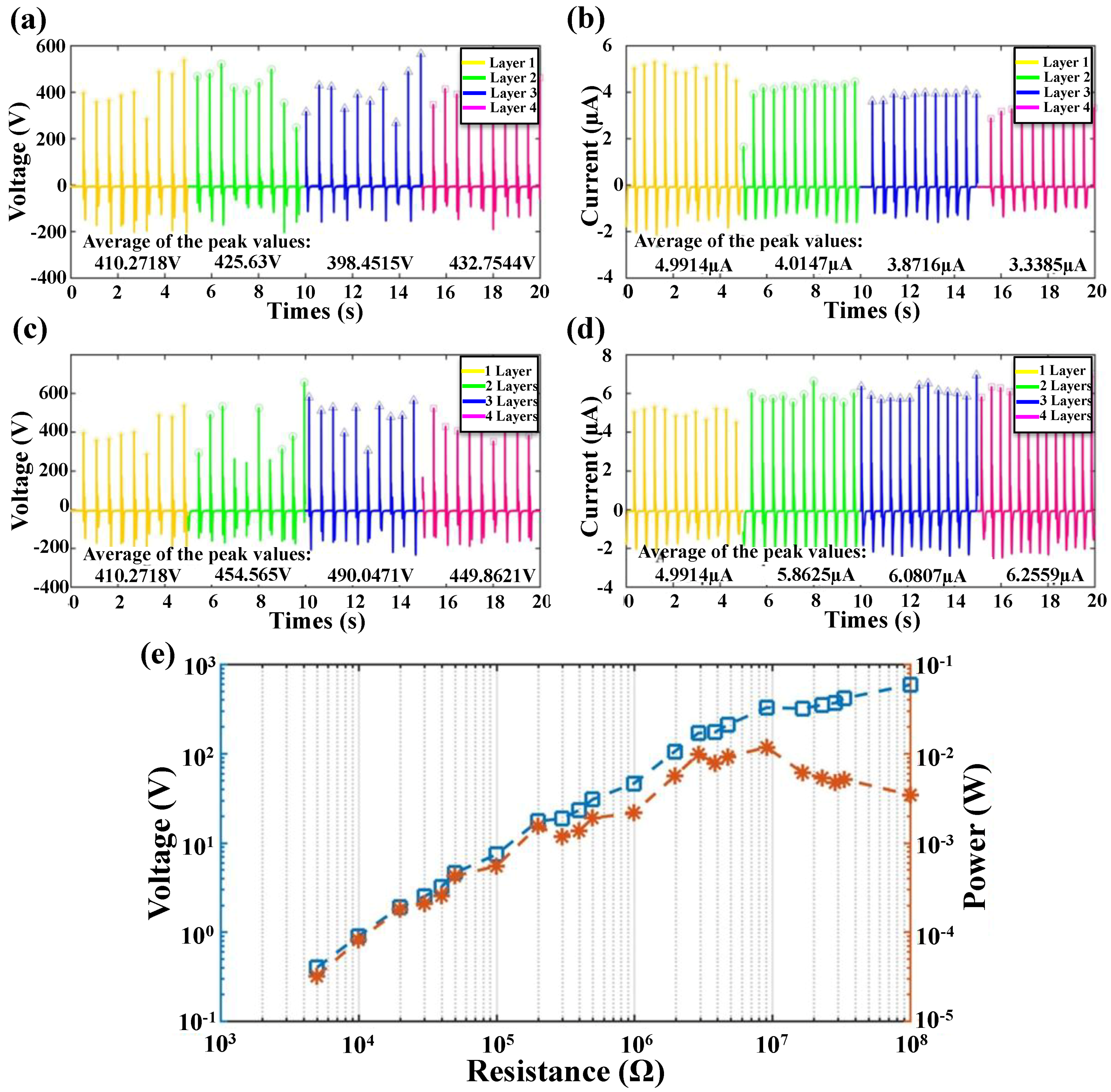
4. Characterization of Energy Harvesting
5. Conclusions
Author Contributions
Funding
Conflicts of Interest
References
- Baytekin, H.T.; Patashinski, A.Z.; Branicki, M.; Baytekin, B.; Soh, S.; Grzybowski, B.A. The mosaic of surface charge in contact electrification. Science 2011, 333, 308–312. [Google Scholar] [CrossRef] [PubMed] [Green Version]
- Schein, L.B. Applied physics. Recent progress and continuing puzzles in electrostatics. Science 2006, 316, 1572–1573. [Google Scholar] [CrossRef] [PubMed]
- Burgo, T.A.L.; Ducati, T.R.D.; Francisco, K.R.; Clinckspoor, K.J.; Galembeck, F.; Galembeck, S.E. Triboelectricity: Macroscopic charge patterns formed by self-arraying ions on polymer surfaces. Langmuir 2012, 28, 7407–7416. [Google Scholar] [CrossRef] [PubMed]
- Dhakar, L.; Tay, F.E.H.; Lee, C. Development of a broadband triboelectric energy harvester with SU-8 micropillars. IEEE/ASME J. Microelectr. Syst. 2015, 24, 91–99. [Google Scholar] [CrossRef]
- Dhakar, L.; Tay, F.E.H.; Lee, C. Investigation of contact electrification based broadband energy harvesting mechanism using elastic PDMS microstructures. J. Micromech. Microeng. 2014, 24. [Google Scholar] [CrossRef]
- Liu, H.; Ji, Z.; Xu, H.; Sun, M.; Chen, T.; Sun, L.; Chen, G.; Wang, Z. Large-scale and flexible self-powered triboelectric tactile sensing array for sensitive robot skin. Polymers 2017, 9, 586. [Google Scholar] [CrossRef]
- Chen, T.; Pan, M.; Wang, Y.; Liu, J.; Chen, L.; Sun, L. Manipulation of microobjects based on dynamic adhesion control. International. J. Adv. Robot. Syst. 2012, 9, 89. [Google Scholar] [CrossRef]
- Liu, H.; Chen, T.; Sun, L.; Lee, C. An Electromagnetic MEMS Energy Harvester Array with Multiple Vibration Modes. Micromachines 2015, 6, 984–992. [Google Scholar] [CrossRef] [Green Version]
- Cheng, X.; Miao, L.; Song, Y.; Su, Z.; Chen, H.; Chen, X.; Zhang, J.; Zhang, H. High efficiency energy management and charge boosting strategy for a triboelectric nanogenerators. Nano Energy 2017, 38, 438–446. [Google Scholar] [CrossRef]
- Chen, H.; Su, Z.; Song, Y.; Cheng, X.; Meng, B.; Song, Z.; Chen, D.; Zhang, H. Omnidirectional bending & pressure sensor based on stretchable CNT-PU sponge. Adv. Funct. Mater. 2016, 27. [Google Scholar] [CrossRef]
- Zhu, G.; Pan, C.F.; Guo, W.X.; Chen, C.; Zhou, Y.S.; Yu, R.M.; Wang, Z.L. Triboelectric-generator-driven pulse electrodeposition for micropatterning. Nano Lett. 2012, 12, 4960–4965. [Google Scholar] [CrossRef] [PubMed]
- Liu, H.; Koh, K.H.; Lee, C. Ultra-wide frequency broadening mechanism for micro-scale electromagnetic energy harvester. Appl. Phys. Lett. 2014, 104, 175–195. [Google Scholar] [CrossRef]
- Zhong, J.W.; Zhang, Q.; Fan, F.R.; Zhang, Y.; Wang, S.H.; Hu, B.; Wang, Z.L.; Zhou, J. Finger typing driven triboelectric nanogenerator and its use for instantaneously lighting up LEDs. Nano Energy 2012, 2, 491–497. [Google Scholar] [CrossRef]
- Wu, Y.; Hu, Y.; Huang, Z.; Lee, C.; Wang, F. Electret-material enhanced triboelectric energy harvesting from air flow for self-powered wireless temperature sensor network. Sens. Actuators A Phys. 2018, 271, 364–372. [Google Scholar] [CrossRef]
- Wang, Z.L.; Chen, J.; Lin, L. Progress in triboelectric nanogenerators as a new energy technology and self-powered sensors. Energy Environ. Sci. 2015, 8, 2250–2282. [Google Scholar] [CrossRef]
- Feng, H.; Zhao, C.; Tan, P.; Liu, R.; Chen, X.; Li, Z. Nanogenerator for biomedical applications. Adv. Healthc. Mater. 2018, 7. [Google Scholar] [CrossRef] [PubMed]
- Park, K.I.; Son, J.H.; Hwang, G.T.; Jeong, C.K.; Ryu, J.; Koo, M.; Choi, I.; Lee, S.H.; Byun, M.; Wang, Z.L.; et al. Nanogenerators: Highly-efficient, flexible piezoelectric PZT thin film nanogenerator on plastic substrates. Adv. Mater. 2014, 26, 2514–2520. [Google Scholar] [CrossRef]
- Kong, J.-H.; Jang, N.-S.; Kim, S.-H.; Kim, J.-M. Simple and rapid micropatterning of conductive carbon composites and its application to elastic strain sensors. Carbon 2014, 77, 199–207. [Google Scholar] [CrossRef]
- Jiang, W.; Li, H.; Liu, Z.; Li, Z.; Tian, J.; Shi, B.; Zou, Y.; Ouyang, H.; Zhao, C.; Zhao, L.; et al. Fully bioabsorbable natural-materials-based triboelectric nanogenerators. Adv. Mater. 2018, 6. [Google Scholar] [CrossRef] [PubMed]
- Fan, F.R.; Tang, W.; Wang, Z.L. Flexible nanogenerators for energy harvesting and self-powered electronics. Adv. Mater. 2016, 28, 4283–4305. [Google Scholar] [CrossRef] [PubMed]
- Li, T.; Li, L.; Sun, H.; Xu, Y.; Wang, X.; Luo, H.; Liu, Z.; Zhang, T. Porous ionic membrane based flexible humidity sensor and its multifunctional applications. Adv. Sci. 2017, 4, 1–7. [Google Scholar] [CrossRef] [PubMed]
- Wang, H.; Wu, H.; Hasan, D.; He, T.; Shi, Q.; Lee, C. Self-powered dual-mode amenity sensor based on the water-air triboelectric nanogenerator. ACS Nano 2017, 11, 10337–10346. [Google Scholar] [CrossRef] [PubMed]
- Yang, Y.; Zhang, H.; Zhong, X.; Yi, F.; Yu, R.; Zhang, Y.; Wang, Z.L. Electret film-enhanced triboelectric nanogenerator matrix for self-powered instantaneous tactile imaging. ACS Appl. Mater. Interfaces 2014, 6, 3680–3688. [Google Scholar] [CrossRef] [PubMed]
- Lin, L.; Xie, Y.; Wang, S.; Wu, W.; Niu, S.; Wen, X.; Wang, Z.L. Triboelectric active sensor array for self-powered static and dynamic pressure detection and tactile imaging. ACS Nano 2013, 7, 8266–8274. [Google Scholar] [CrossRef] [PubMed]
- Chen, T.; Shi, Q.; Yang, Z.; Liu, J.; Liu, H.; Sun, L.; Lee, C. A Self-Powered Six-Axis Tactile Sensor by Using Triboelectric Mechanism. Nanomaterials 2018, 8, 503. [Google Scholar] [CrossRef] [PubMed]
- Zhou, Y.S.; Zhu, G.; Niu, S.; Liu, Y.; Bai, P.; Jing, Q.; Wang, Z.L. Nanometer resolution self-powered static and dynamic motion sensor based on micro-grated triboelectrification. Adv. Mater. 2014, 26, 1719–1724. [Google Scholar] [CrossRef] [PubMed]
- Jing, Q.; Zhu, G.; Wu, W.; Bai, P.; Xie, Y.; Han, R.P.; Wang, Z.L. Self-powered triboelectric velocity sensor for dual-mode sensing of rectified linear and rotary motions. Nano Energy 2014, 10, 305–312. [Google Scholar] [CrossRef]
- Chen, T.; Xia, Y.; Liu, W.; Liu, H.; Sun, L.; Lee, C. A Hybrid flapping-blade wind energy harvester based on vortex shedding effect. J. Microelectromech. Syst. 2016, 25, 845–847. [Google Scholar] [CrossRef]
- Lin, L.; Wang, S.; Niu, S.; Liu, C.; Xie, Y.; Wang, Z.L. Noncontact free-rotating disk triboelectric nanogenerator as a sustainable energy harvester and self-powered mechanical sensor. ACS Appl. Mater. Interfaces 2014, 6, 3031–3038. [Google Scholar] [CrossRef] [PubMed]
- Chen, T.; Zhao, M.; Shi, Q.; Yang, Z.; Liu, H.; Sun, L.; Ouyang, J.; Lee, C. Novel augmented reality interface using a self-powered triboelectric based virtual reality 3D-control sensor. Nano Energy 2018, 51, 162–172. [Google Scholar] [CrossRef]
- Evans, D. The Internet of Things: How the Next Evolution of the Internet Is Changing Everything; CISCO White Paper; CISCO Internet Business Solutions Group (IBSG): San Jose, CA, USA, 2011; pp. 1–11. [Google Scholar]
- Yang, Y.; Zhou, Y.S.; Zhang, H.; Liu, Y.; Lee, S.; Wang, Z.L. A single-electrode based triboelectric nanogenerator as self-powered tracking system. Adv. Mater. 2013, 25, 6594–6601. [Google Scholar] [CrossRef] [PubMed]
- Zhu, G.; Yang, W.Q.; Zhang, T.; Jing, Q.; Chen, J.; Zhou, Y.S.; Bai, P.; Wang, Z.L. Self-powered, ultrasensitive, flexible tactile sensors based on contact electrification. Nano Lett. 2014, 14, 3208–3213. [Google Scholar] [CrossRef] [PubMed]
- Shi, Q.; Wang, H.; Wu, H.; Lee, C. Self-powered triboelectric nanogenerator buoy ball for applications ranging from environment monitoring to water wave energy farm. Nano Energy 2017, 40, 203–213. [Google Scholar] [CrossRef]
- Cao, Y.; Li, T.; Gu, Y.; Luo, H.; Wang, S.; Zhang, T. Fingerprint-inspired flexible tactile sensor for accurately discerning surface texture. Small 2018, 14. [Google Scholar] [CrossRef] [PubMed]
- Li, G.; Liu, L.; Wu, G.; Chen, W.; Qin, S.; Wang, Y.; Zhang, T. Self-powered UV–near infrared photodetector based on reduced graphene oxide/n-Si vertical heterojunction. Small 2016, 12, 5019–5026. [Google Scholar] [CrossRef] [PubMed]
- Yi, F.; Lin, L.; Niu, S.; Yang, J.; Wu, W.; Wang, S.; Liao, Q.; Zhang, Y.; Wang, Z.L. Self-powered trajectory, velocity, and acceleration tracking of a moving object/body using a triboelectric sensor. Adv. Funct. Mater. 2014, 24, 7488–7494. [Google Scholar] [CrossRef]
- Shi, Q.; Wang, H.; Wang, T.; Lee, C. Self-powered liquid triboelectric microfluidic sensor for pressure sensing and finger motion monitoring applications. Nano Energy 2016, 30, 450–459. [Google Scholar] [CrossRef]
- Meng, B.; Tang, W.; Too, Z.H.; Zhang, X.; Han, M.; Liu, W.; Zhang, H. A transparent single-friction-surface triboelectric generator and self-powered touch sensor. Energy Environ. Sci. 2013, 6, 3235–3240. [Google Scholar] [CrossRef]
- Li, Z.; Chen, J.; Guo, H.; Fan, X.; Wen, Z.; Yeh, M.H.; Yu, C.; Cao, X.; Wang, Z.L. Triboelectrification-Enabled Self-Powered Detection and Removal of Heavy Metal Ions in Wastewater. Adv. Mater. 2016, 28, 2983–2991. [Google Scholar] [CrossRef] [PubMed]
- Peng, W.; Yu, R.; He, Y.; Wang, Z.L. Theoretical study of triboelectric-potential gated/driven metal–oxide–semiconductor field-effect transistor. ACS Nano 2016, 10, 4395–4402. [Google Scholar] [CrossRef] [PubMed]
- Alam, M.A.; Varghese, D.; Kaczer, B. Theory of breakdown position determination by voltage- and current-ratio methods. IEEE Trans. Electron. Devices 2008, 55, 3150–3158. [Google Scholar] [CrossRef]
- Kim, C.; Lee, H.; Oh, K.H.; Sun, J. Highly stretchable, transparent ionic touch panel. Science 2016, 353, 682–687. [Google Scholar] [CrossRef] [PubMed]
- Shi, M.; Zhang, J.; Chen, H.; Han, M.; Shankaregowda, S.A.; Su, Z.; Meng, B.; Cheng, X.; Zhang, H. Self-powered analogue smart skin. ACS Nano 2016, 10, 4083–4091. [Google Scholar] [CrossRef] [PubMed]
- Li, T.; Zou, J.; Xing, F.; Zhang, M.; Cao, X.; Wang, N.; Wang, Z.L. From Dual-Mode triboelectric nanogenerator to smart tactile sensor: A multiplexing design. ACS Nano 2017, 11, 3950–3956. [Google Scholar] [CrossRef] [PubMed]
- Liu, H.; Zhang, J.; Shi, Q.; He, T.; Chen, T.; Sun, L.; Dziuban, J.A.; Lee, C. Development of a thermoelectric and electromagnetic hybrid energy harvester from water flow in irrigation system. Micromachines 2018, 9, 395. [Google Scholar] [CrossRef]
- Han, M.; Zhang, X.; Sun, X.; Meng, B.; Liu, W.; Zhang, H. Magnetic-assisted triboelectric nanogenerators as self-powered visualized omnidirectional tilt sensing system. Sci. Rep. 2014, 4, 4811. [Google Scholar] [CrossRef] [PubMed] [Green Version]
- Yang, Y.; Zhang, H.; Lin, Z.-H.; Zhou, Y.S.; Jing, Q.; Su, Y.; Yang, J.; Chen, J.; Hu, C.; Wang, Z.L. Human skin based triboelectric nanogenerators for harvesting biomechanical energy and as self-powered active tactile sensor system. ACS Nano 2013, 7, 9213–9222. [Google Scholar] [CrossRef] [PubMed]
- Fan, F.-R.; Lin, L.; Zhu, G.; Wu, W.; Zhang, R.; Wang, Z.L. Transparent triboelectric nanogenerators and self-powered pressure sensors based on micropatterned plastic films. Nano Lett. 2012, 12, 3109–3114. [Google Scholar] [CrossRef] [PubMed]
- Kim, S.; Gupta, M.K.; Lee, K.Y.; Sohn, A.; Kim, T.Y.; Shin, K.-S.; Kim, D.; Kim, S.K.; Lee, K.H.; Shin, H.-J.; et al. Transparent flexible graphene triboelectric nanogenerators. Adv. Mater. 2014, 26, 3918–3925. [Google Scholar] [CrossRef] [PubMed]
- Zhang, X.-S.; Han, M.-D.; Wang, R.-X.; Meng, B.; Zhu, F.-Y.; Sun, X.-M.; Hu, W.; Wang, W.; Li, Z.-H.; Zhang, H.-X. High-performance triboelectric nanogenerator with enhanced energy density based on single-step fluorocarbon plasma treatment. Nano Energy 2014, 4, 123–131. [Google Scholar] [CrossRef]
- Liu, H.; Ji, Z.; Chen, T.; Sun, L.; Menon, S.C.; Lee, C. An Intermittent Self-Powered Energy Harvesting System from Low-Frequency Hand Shaking. IEEE Sens. J. 2015, 15, 4782–4790. [Google Scholar] [CrossRef]
- Zhang, X.-S.; Han, M.-D.; Wang, R.-X.; Zhu, F.-Y.; Li, Z.-H.; Wang, W.; Zhang, H.-X. Frequency-multiplication high-output triboelectric nanogenerator for sustainably powering biomedical microsystems. Nano Lett. 2013, 13, 1168–1172. [Google Scholar] [CrossRef] [PubMed]
- Zhang, X.-S.; Han, M.-D.; Meng, B.; Zhang, H.-X. High performance triboelectric nanogenerators based on large-scale mass-fabrication technologies. Nano Energy 2015, 11, 304–322. [Google Scholar] [CrossRef]
- Niu, S.; Liu, Y.; Wang, S.; Lin, L.; Zhou, Y.S.; Hu, Y.; Wang, Z.L. Theoretical investigation and structural optimization of single-electrode triboelectric nanogenerators. Adv. Funct. Mater. 2014, 24, 3332–3340. [Google Scholar] [CrossRef]
- Lee, S.H.; Wang, H.; Shi, Q.; Dhakar, L.; Wang, J.; Thakor, N.V.; Yen, S.C.; Lee, C. Development of battery-free neural interface and modulated control of tibialis anterior muscle via common peroneal nerve based on triboelectric nanogenerators (TENGs). Nano Energy 2017, 33, 1–11. [Google Scholar] [CrossRef]
- Hassani, F.A.; Mogan, R.P.; Gammad, G.G.L.; Wang, H.; Yen, S.C.; Thakor, N.V.; Lee, C. Toward a self-control system for a neurogenic underactive bladder—A triboelectric nanogenerator sensor integrated with a bi-Stable micro-actuator. ACS Nano 2018, 12, 3487–3501. [Google Scholar] [CrossRef] [PubMed]
- Diaz, A.F.; Felix-Navarro, R.M. A semi-quantitative tribo-electric series for polymeric materials: The influence of chemical structure and properties. J. Electrost. 2004, 62, 277–290. [Google Scholar] [CrossRef]
- Wang, Q.; Chen, M.; Li, W.; Li, Z.; Chen, Y.; Zhai, Y. Size effect on the output of a miniaturized triboelectric nanogenerator based on superimposed electrode layers. Nano Energy 2017, 41, 128–138. [Google Scholar] [CrossRef]


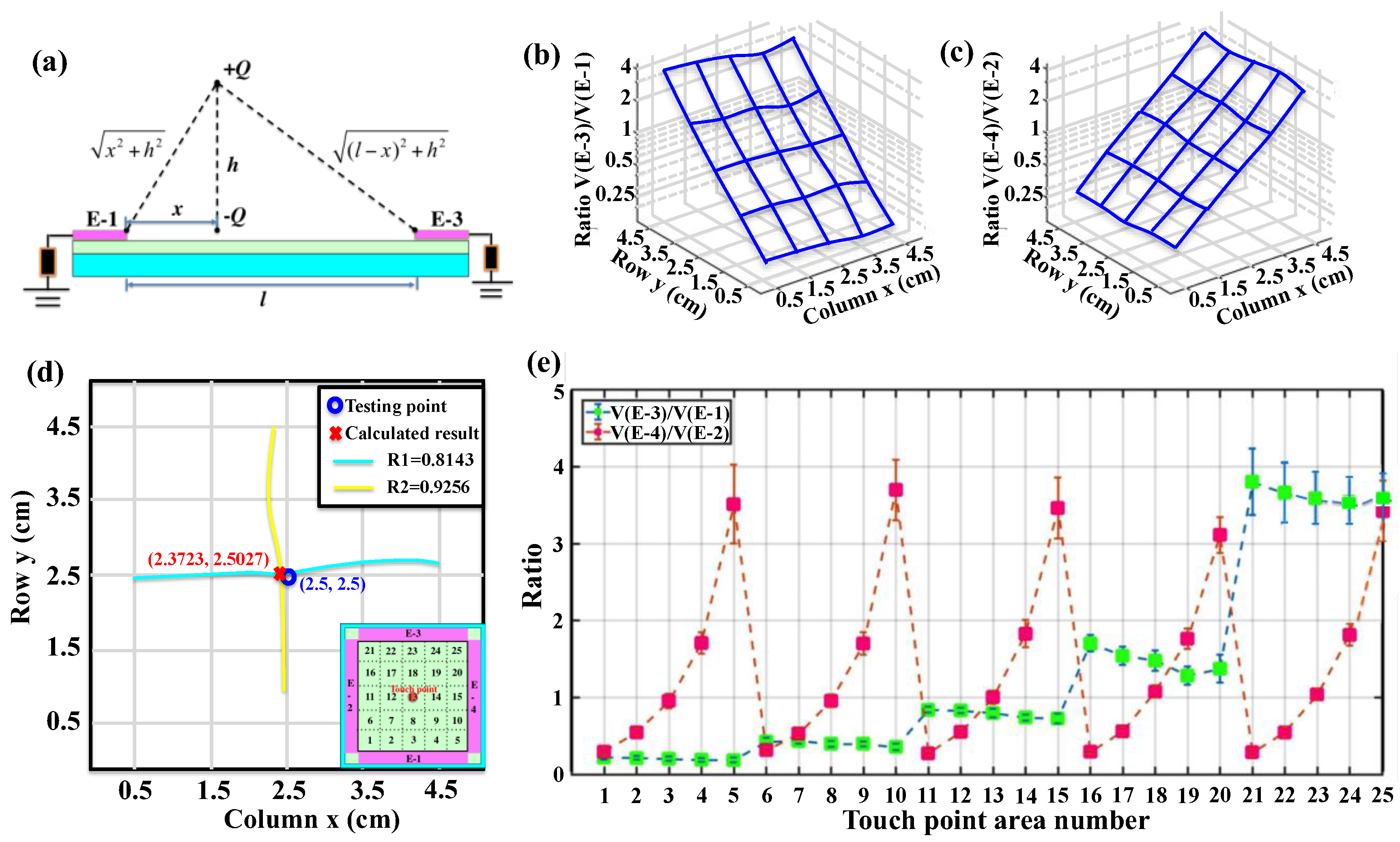
| x = 0.5 | x = 1.5 | x = 2.5 | x = 3.5 | x = 4.5 | |
|---|---|---|---|---|---|
| y = 4.5 | 3.8004 | 3.6505 | 3.3684 | 2.889 | 3.1085 |
| y = 3.5 | 1.703 | 1.5404 | 1.4802 | 1.2836 | 1.3732 |
| y = 2.5 | 0.8411 | 0.8294 | 0.7971 | 0.7378 | 0.7274 |
| y = 1.5 | 0.4265 | 0.4359 | 0.397 | 0.3972 | 0.3578 |
| y = 0.5 | 0.2225 | 0.2152 | 0.2044 | 0.1887 | 0.1876 |
| x = 0.5 | x = 1.5 | x = 2.5 | x = 3.5 | x = 4.5 | |
|---|---|---|---|---|---|
| y = 4.5 | 0.2867 | 0.5472 | 1.0378 | 1.8145 | 3.4459 |
| y = 3.5 | 0.2934 | 0.5613 | 1.0762 | 1.7614 | 3.1086 |
| y = 2.5 | 0.2763 | 0.5526 | 1.0027 | 1.8276 | 3.4593 |
| y = 1.5 | 0.3163 | 0.5312 | 0.9572 | 1.6986 | 3.6931 |
| y = 0.5 | 0.2976 | 0.5463 | 0.9545 | 1.7053 | 3.5104 |
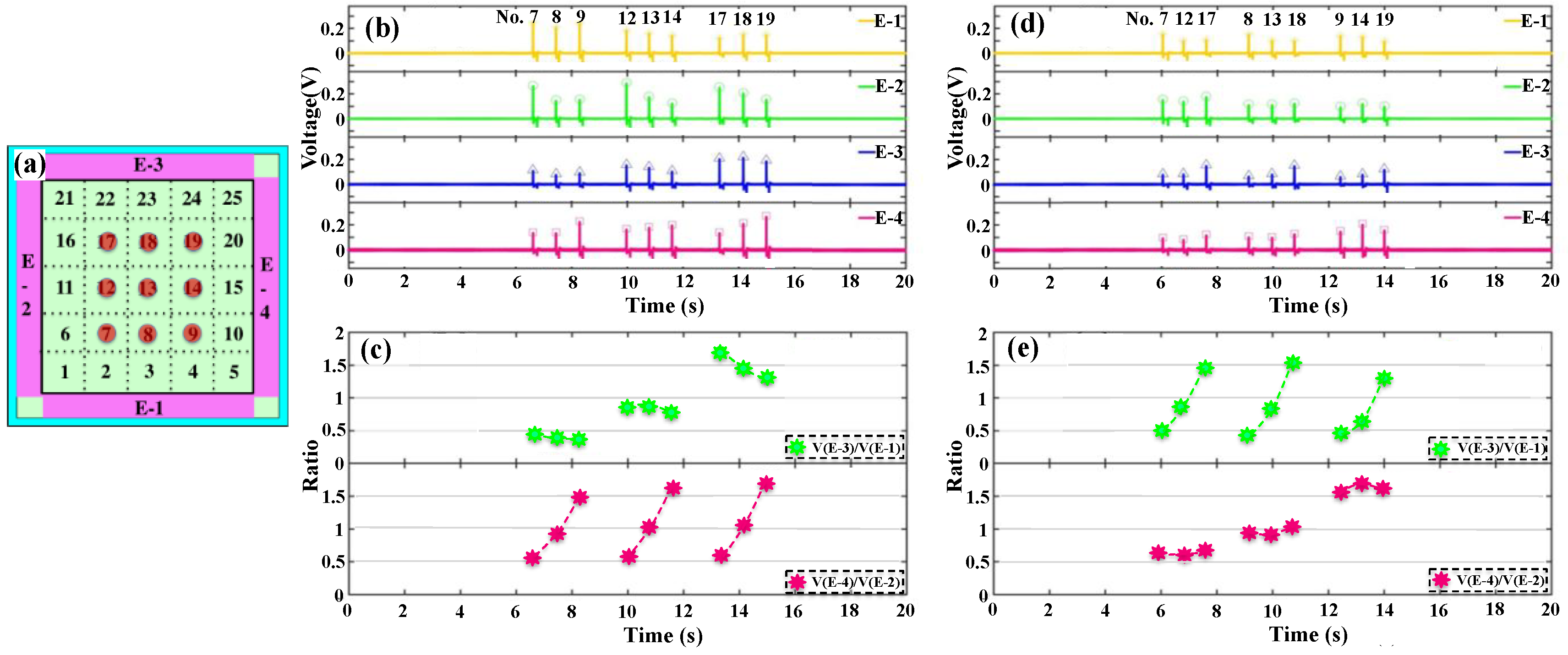
| Voltage Ratios | No. 7 | No. 8 | No. 9 | No. 12 | No. 13 | No. 14 | No. 17 | No. 18 | No. 19 |
|---|---|---|---|---|---|---|---|---|---|
| V(E-3)/V(E-1) | 0.4512 | 0.3805 | 0.386 | 0.8588 | 0.8728 | 0.7605 | 1.7273 | 1.455 | 1.2955 |
| V(E-4)/V(E-2) | 0.5299 | 0.9294 | 1.4623 | 0.5837 | 1.0252 | 1.6991 | 0.5472 | 1.0273 | 1.7275 |
| Voltage Ratios | No. 7 | No. 12 | No. 17 | No. 8 | No. 13 | No. 18 | No. 9 | No. 14 | No. 19 |
|---|---|---|---|---|---|---|---|---|---|
| V(E-3)/V(E-1) | 0.5218 | 0.8475 | 1.4187 | 0.4418 | 0.8143 | 1.5311 | 0.4536 | 0.6301 | 1.2824 |
| V(E-4)/V(E-2) | 0.6295 | 0.6035 | 0.6796 | 0.9333 | 0.9014 | 1.0386 | 1.5705 | 1.6925 | 1.6028 |
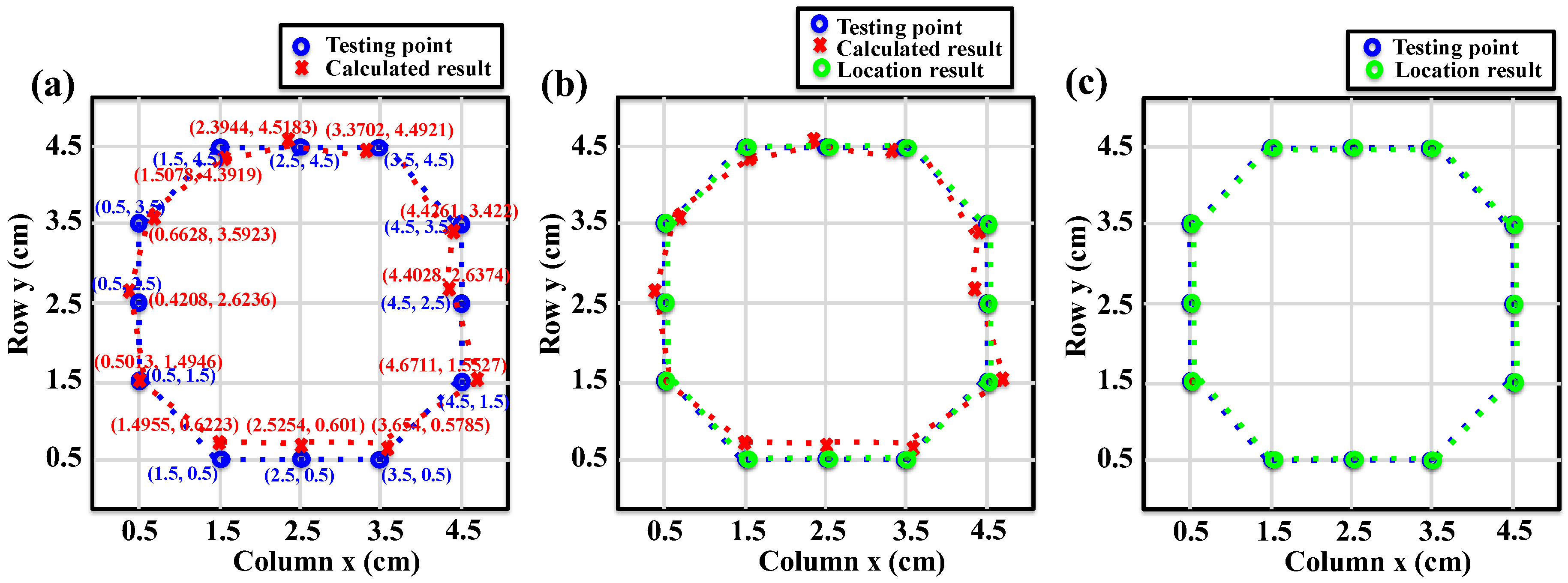
| Voltage Ratios | No. 23 | No. 22 | No. 16 | No. 11 | No. 6 | No. 2 | No. 3 | No. 4 | No. 10 | No. 15 | No. 20 | No. 24 |
|---|---|---|---|---|---|---|---|---|---|---|---|---|
| V(E-3)/V(E-1) | 4.7561 | 3.9515 | 1.9747 | 1.0719 | 0.4253 | 0.2991 | 0.2153 | 0.2454 | 0.583 | 1.098 | 1.9238 | 4.5863 |
| V(E-4)/V(E-2) | 1.6412 | 0.7526 | 0.2696 | 0.3359 | 0.2296 | 0.5009 | 0.9345 | 1.9636 | 4.9517 | 4.1615 | 4.9946 | 2.5985 |
© 2018 by the authors. Licensee MDPI, Basel, Switzerland. This article is an open access article distributed under the terms and conditions of the Creative Commons Attribution (CC BY) license (http://creativecommons.org/licenses/by/4.0/).
Share and Cite
Chen, T.; Shi, Q.; Li, K.; Yang, Z.; Liu, H.; Sun, L.; Dziuban, J.A.; Lee, C. Investigation of Position Sensing and Energy Harvesting of a Flexible Triboelectric Touch Pad. Nanomaterials 2018, 8, 613. https://doi.org/10.3390/nano8080613
Chen T, Shi Q, Li K, Yang Z, Liu H, Sun L, Dziuban JA, Lee C. Investigation of Position Sensing and Energy Harvesting of a Flexible Triboelectric Touch Pad. Nanomaterials. 2018; 8(8):613. https://doi.org/10.3390/nano8080613
Chicago/Turabian StyleChen, Tao, Qiongfeng Shi, Kunpu Li, Zhan Yang, Huicong Liu, Lining Sun, Jan A. Dziuban, and Chengkuo Lee. 2018. "Investigation of Position Sensing and Energy Harvesting of a Flexible Triboelectric Touch Pad" Nanomaterials 8, no. 8: 613. https://doi.org/10.3390/nano8080613
APA StyleChen, T., Shi, Q., Li, K., Yang, Z., Liu, H., Sun, L., Dziuban, J. A., & Lee, C. (2018). Investigation of Position Sensing and Energy Harvesting of a Flexible Triboelectric Touch Pad. Nanomaterials, 8(8), 613. https://doi.org/10.3390/nano8080613