Spin-Coated CH3NH3PbBr3 Film Consisting of Micron-Scale Single Crystals Assisted with a Benzophenone Crystallizing Agent and Its Application in Perovskite Light-Emitting Diodes


Abstract
:1. Introduction
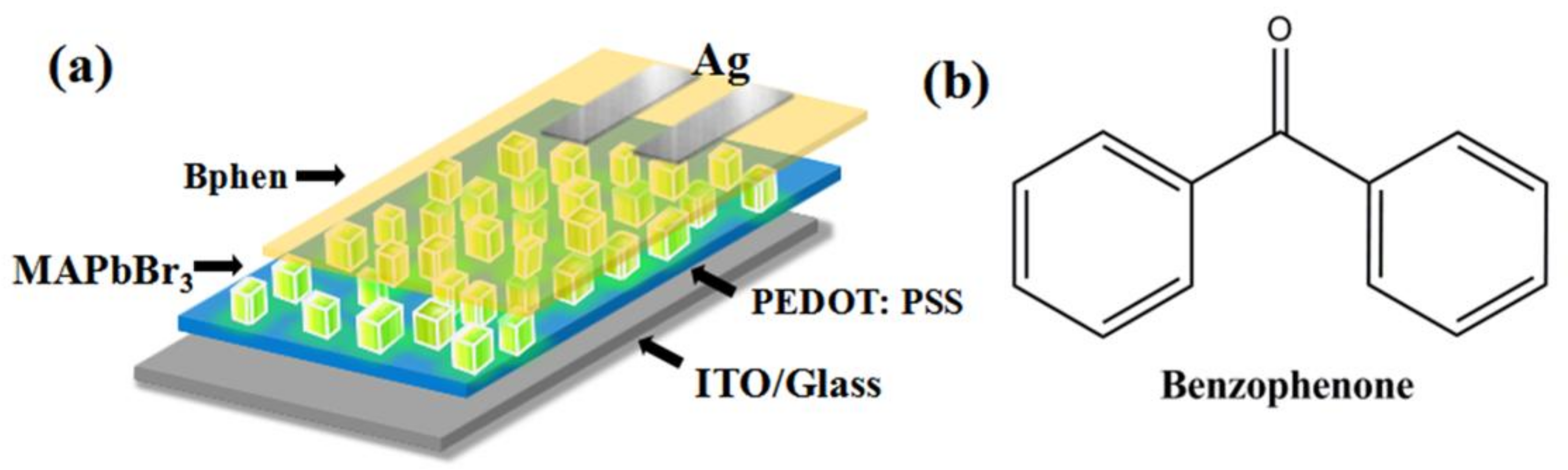
2. Experimental
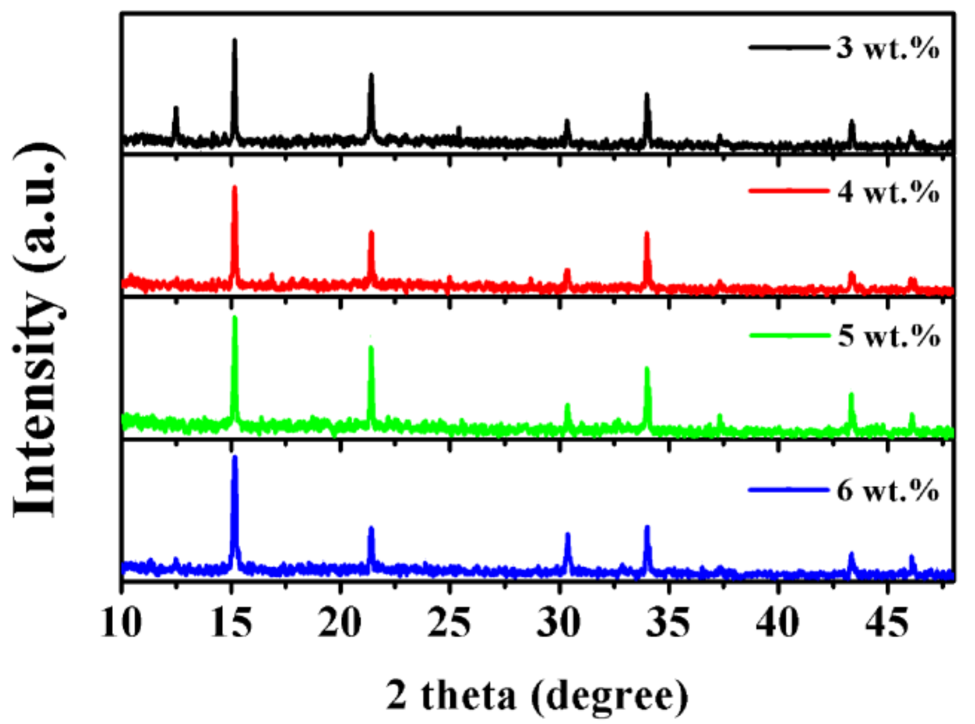
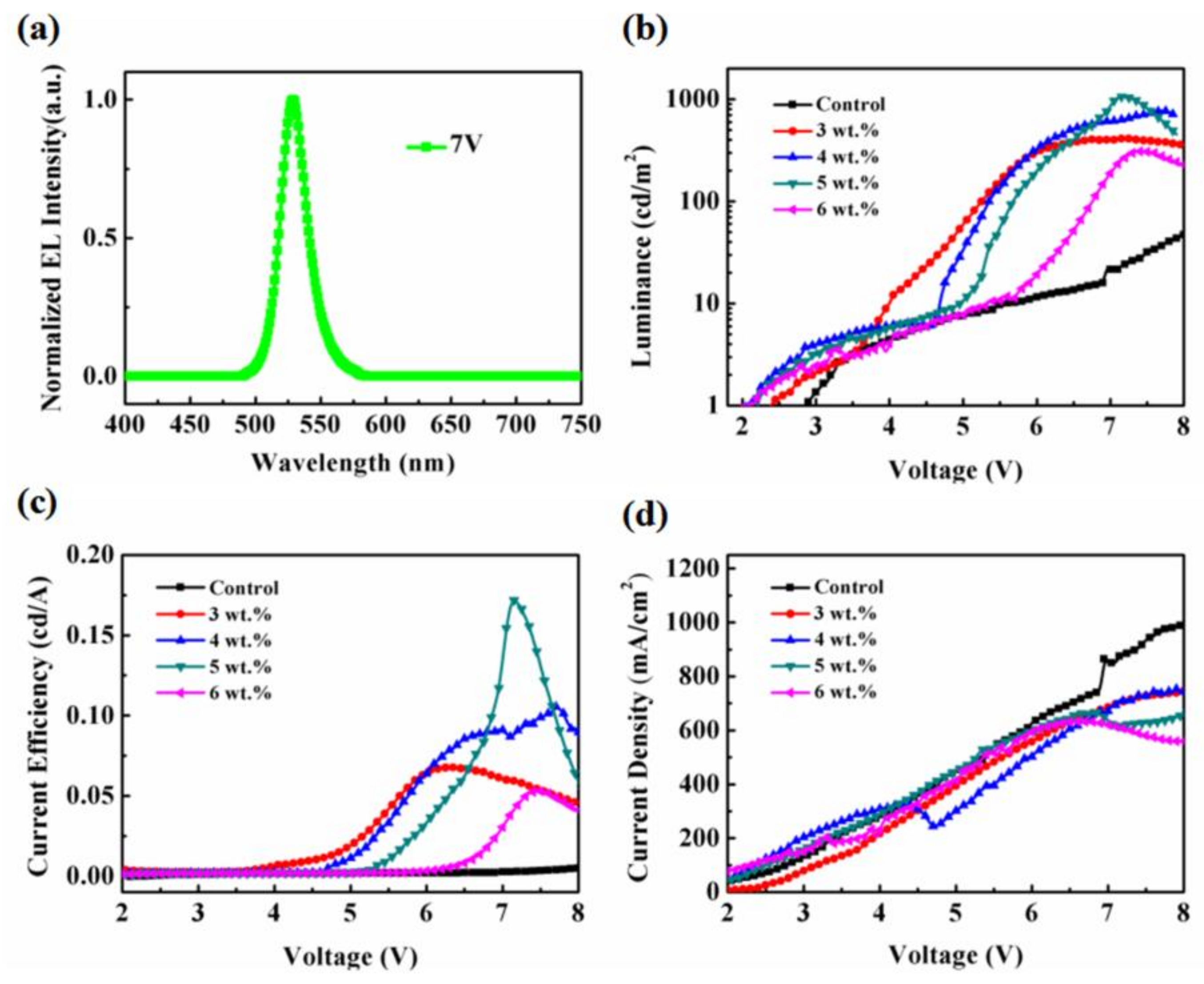
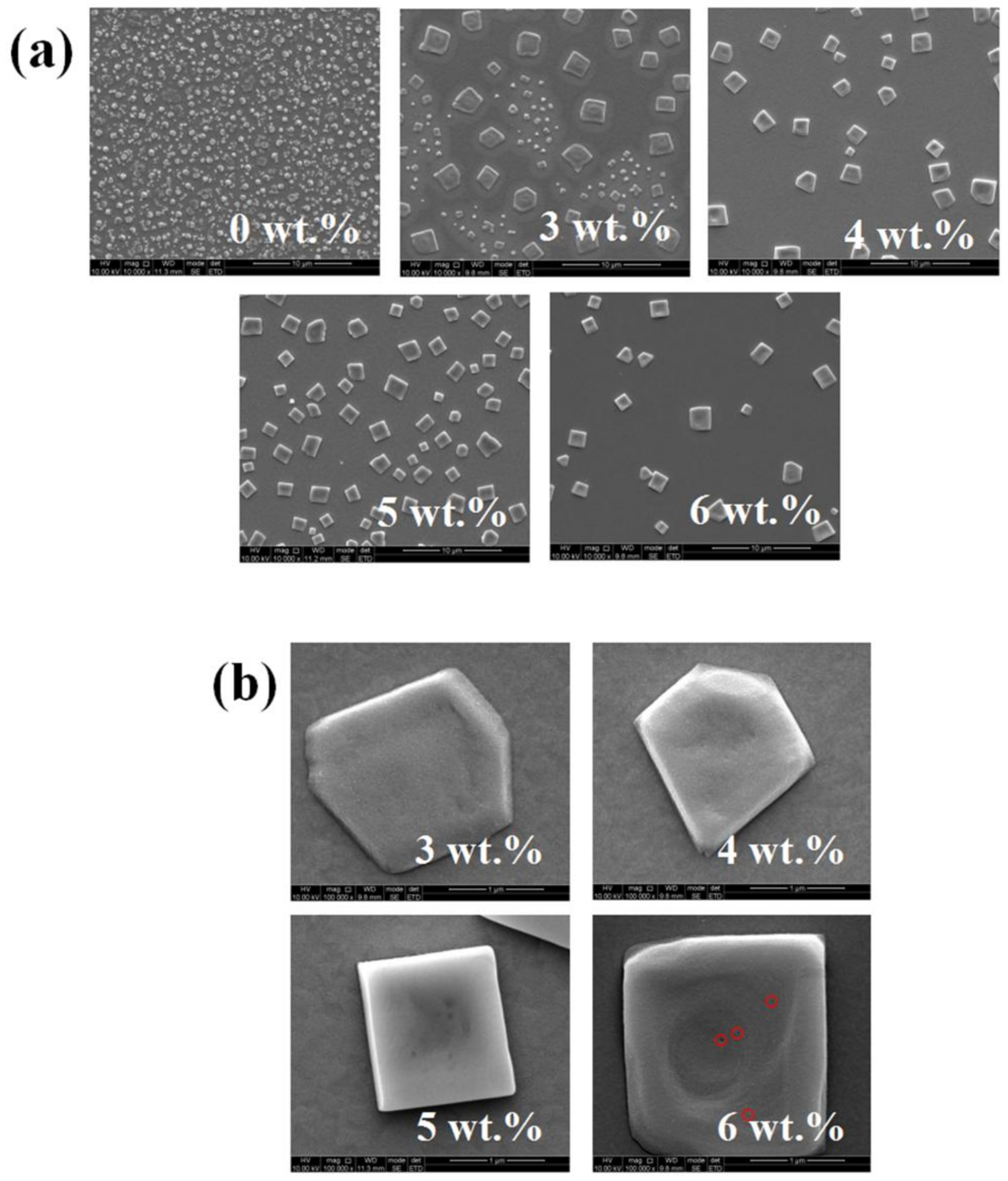
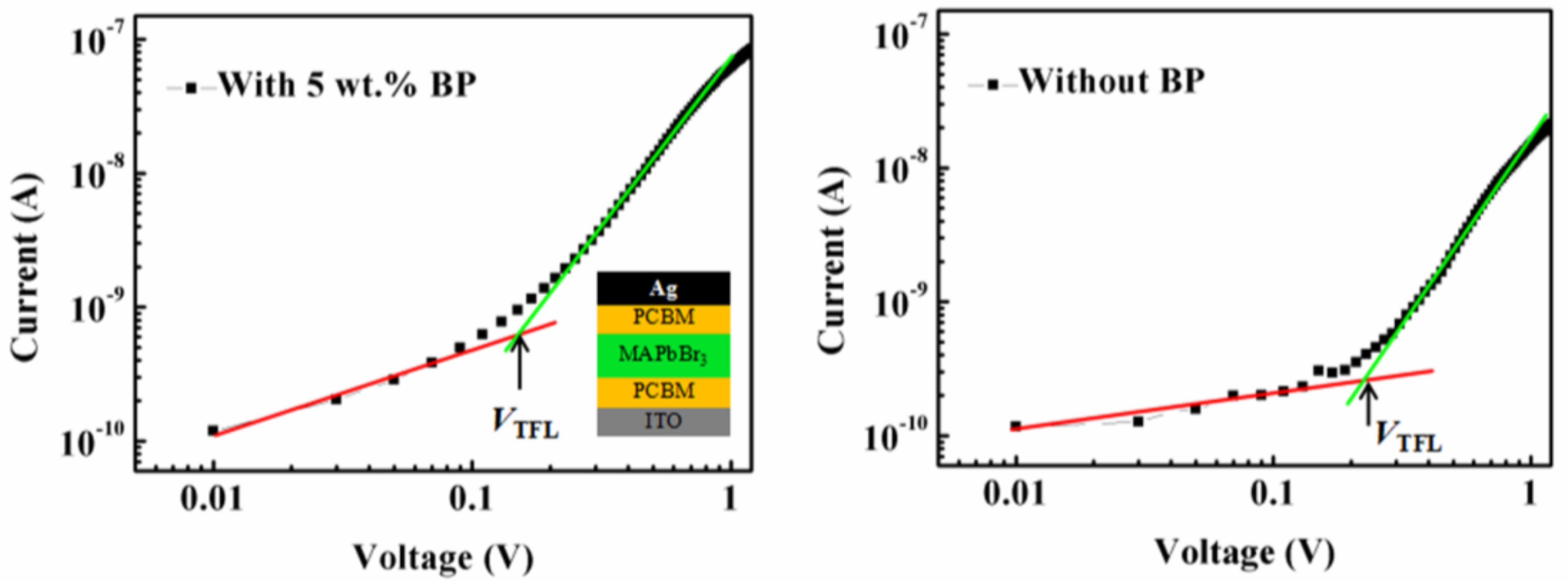
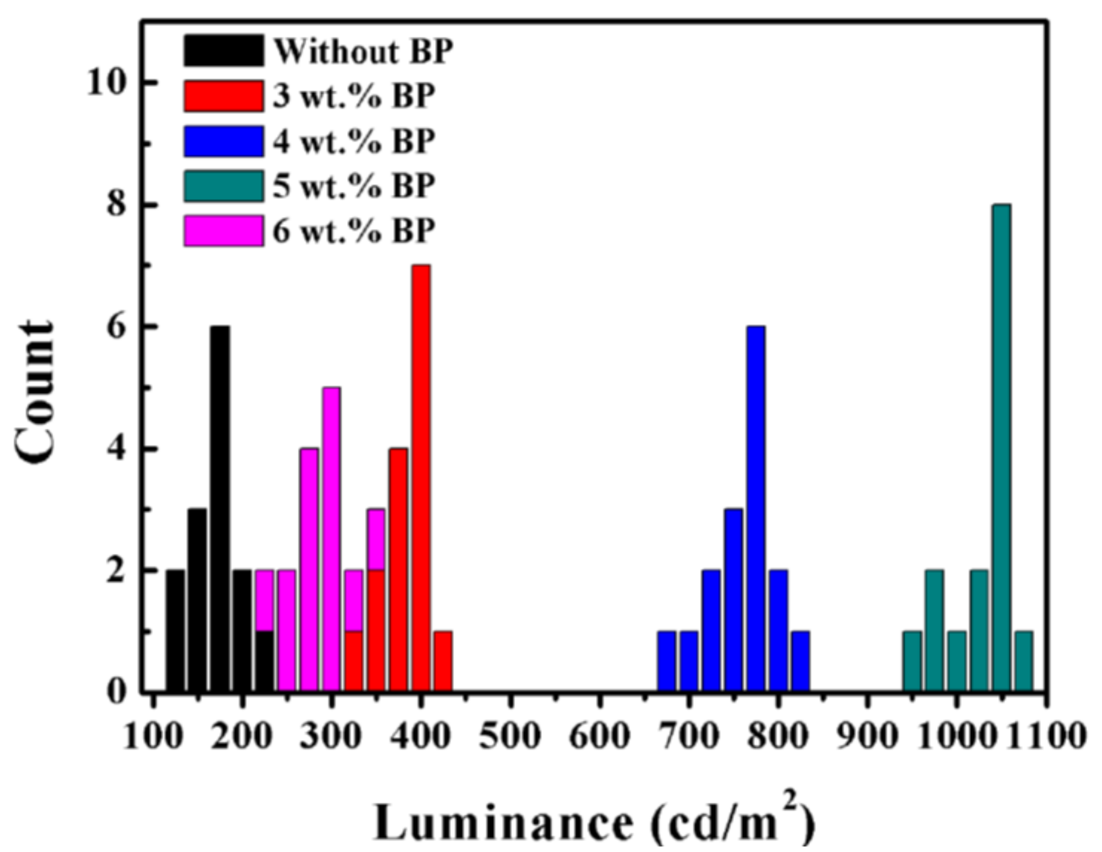
3. Results and Discussion
4. Conclusions
Supplementary Materials
Author Contributions
Acknowledgments
Conflicts of Interest
References
- Yang, W.S.; Noh, J.H.; Jeon, N.; Kim, Y.C.; Ryu, S.; Seo, J.; Seok, S.I. High-performance photovoltaic perovskite layers fabricated through intramolecular exchange. Science 2015, 348, 1234–1237. [Google Scholar] [CrossRef] [PubMed]
- Xing, G.; Mathews, N.; Lim, S.S.; Yantara, N.; Liu, X.; Sabba, D.; Gratzel, M.; Mhaisalkar, S.; Sum, T.C. Low-temperature solution-processed wavelength-tunable perovskites for lasing. Nat. Mater. 2014, 13, 476–480. [Google Scholar] [CrossRef] [PubMed]
- Wang, N.; Cheng, L.; Ge, R.; Zhang, S.; Miao, Y.; Zou, W.; Yi, C.; Sun, Y.; Cao, Y.; Yang, R.; et al. Perovskite light-emitting diodes based on solution-processed self-organized multiple quantum wells. Nat. Photonics 2016, 10, 699–704. [Google Scholar] [CrossRef] [Green Version]
- Lee, M.M.; Teuscher, J.; Miyasaka, T.; Murakami, T.N.; Snaith, H.J. Efficient hybrid solar cells based on meso-superstructured organometal halide perovskites. Science 2012, 338, 643–647. [Google Scholar] [CrossRef] [PubMed]
- Zheng, Y.; Kong, J.; Huang, D.; Shi, W.; McMillon-Brown, L.; Katz, H.E.; Yu, J.; Taylor, A.D. Spray coating of the pcbm electron transport layer significantly improves the efficiency of p-i-n planar perovskite solar cells. Nanoscale 2018, 10, 11342–11348. [Google Scholar] [CrossRef] [PubMed]
- Wang, Z.; Li, Z.; Zhou, D.; Yu, J. Low turn-on voltage perovskite light-emitting diodes with methanol treated pedot:Pss as hole transport layer. Appl. Phys. Lett. 2017, 111, 233304. [Google Scholar] [CrossRef]
- Zheng, Y.; Shi, W.; Kong, J.; Huang, D.; Katz, H.E.; Yu, J.; Taylor, A.D. A cytop insulating tunneling layer for efficient perovskite solar cells. Small Methods 2017, 1, 1700244. [Google Scholar] [CrossRef]
- Zou, W.; Li, R.; Zhang, S.; Liu, Y.; Wang, N.; Cao, Y.; Miao, Y.; Xu, M.; Guo, Q.; Di, D.; et al. Minimising efficiency roll-off in high-brightness perovskite light-emitting diodes. Nat. Commun. 2018, 9, 608; [Google Scholar] [CrossRef] [PubMed]
- Zheng, D.; Yang, G.; Zheng, Y.; Fan, P.; Ji, R.; Huang, J.; Zhang, W.; Yu, J. Carbon nano-onions as a functional dopant to modify hole transporting layers for improving stability and performance of planar perovskite solar cells. Electrochimica Acta 2017, 247, 548–557. [Google Scholar] [CrossRef]
- Shi, Y.; Wu, W.; Dong, H.; Li, G.R.; Xi, K.; Divitini, G.; Ran, C.; Yuan, F.; Zhang, M.; Jiao, B.; et al. A strategy for architecture design of crystalline perovskite light-emitting diodes with high performance. Adv. Mater. 2018, 30, 1800251. [Google Scholar] [CrossRef] [PubMed]
- Wenger, B.; Nayak, P.K.; Wen, X.; Kesava, S.V.; Noel, N.K.; Snaith, H.J. Consolidation of the optoelectronic properties of ch3nh3pbbr3 perovskite single crystals. Nat. Commun. 2017, 8, 590. [Google Scholar] [CrossRef] [PubMed]
- Huang, J.; Shao, Y.; Dong, Q. Organometal trihalide perovskite single crystals: A next wave of materials for 25% efficiency photovoltaics and applications beyond? J. Phys. Chem. Lett. 2015, 6, 3218–3227. [Google Scholar] [CrossRef]
- Luo, Y.; Khoram, P.; Brittman, S.; Zhu, Z.; Lai, B.; Ong, S.P.; Garnett, E.C.; Fenning, D.P. Direct observation of halide migration and its effect on the photoluminescence of methylammonium lead bromide perovskite single crystals. Adv. Mater. 2017, 29, 1703451. [Google Scholar] [CrossRef] [PubMed]
- Liu, Y.; Yang, Z.; Cui, D.; Ren, X.; Sun, J.; Liu, X.; Zhang, J.; Wei, Q.; Fan, H.; Yu, F.; et al. Two-inch-sized perovskite ch3 nh3 pbx3 (x = cl, br, i) crystals: Growth and characterization. Adv. Mater. 2015, 27, 5176–5183. [Google Scholar] [CrossRef] [PubMed]
- Lee, S.; Park, J.H.; Nam, Y.S.; Lee, B.R.; Zhao, B.; Di Nuzzo, D.; Jung, E.D.; Jeon, H.; Kim, J.Y.; Jeong, H.Y.; et al. Growth of nanosized single crystals for efficient perovskite light-emitting diodes. ACS Nano 2018, 12, 3417–3423. [Google Scholar] [CrossRef] [PubMed]
- Shi, D.; Adinolfi, V.; Comin, R.; Yuan, M.; Alarousu, E.; Buin, A.; Chen, Y.; Hoogland, S.; Rothenberger, A.; Katsiev, K.; et al. Low trap-state density and long carrier diffusion in organolead trihalide perovskite single crystals. Science 2015, 347, 519–522. [Google Scholar] [CrossRef] [PubMed] [Green Version]
- Dong, Q.; Fang, Y.; Shao, Y.; Mulligan, P.; Qiu, J.; Cao, L.; Huang, J. Electron-hole diffusion lengths > 175 µm in solution-grown CH3NH3PbI3 single crystals. Science 2015, 347, 967–969. [Google Scholar] [CrossRef] [PubMed]
- Chen, Y.X.; Ge, Q.Q.; Shi, Y.; Liu, J.; Xue, D.J.; Ma, J.Y.; Ding, J.; Yan, H.J.; Hu, J.S.; Wan, L.J. General space-confined on-substrate fabrication of thickness-adjustable hybrid perovskite single-crystalline thin films. J. Am. Chem. Soc. 2016, 138, 16196–16199. [Google Scholar] [CrossRef] [PubMed]
- Liu, X.; Liu, Y.; Gao, F.; Yang, Z.; Liu, S. Photoinduced surface voltage mapping study for large perovskite single crystals. Appl. Phys. Lett. 2016, 108, 181604. [Google Scholar] [CrossRef]
- Saidaminov, M.I.; Adinolfi, V.; Comin, R.; Abdelhady, A.L.; Peng, W.; Dursun, I.; Yuan, M.; Hoogland, S.; Sargent, E.H.; Bakr, O.M. Planar-integrated single-crystalline perovskite photodetectors. Nat. Commun. 2015, 6, 8724. [Google Scholar] [CrossRef] [PubMed] [Green Version]
- Poglitsch, A.; Weber, D. Dynamic disorder in methylammoniumtrihalogenoplumbates (II) observed by millimeter-wave spectroscopy. J. Chem. Phys. 1987, 87, 6373–6378. [Google Scholar] [CrossRef]
- Saidaminov, M.I.; Abdelhady, A.L.; Murali, B.; Alarousu, E.; Burlakov, V.M.; Peng, W.; Dursun, I.; Wang, L.; He, Y.; Maculan, G.; et al. High-quality bulk hybrid perovskite single crystals within minutes by inverse temperature crystallization. Nat. Commun. 2015, 6, 7586. [Google Scholar] [CrossRef] [PubMed] [Green Version]
- Kadro, J.M.; Nonomura, K.; Gachet, D.; Gratzel, M.; Hagfeldt, A. Facile route to freestanding ch3nh3pbi3 crystals using inverse solubility. Sci. Rep. 2015, 5, 11654. [Google Scholar] [CrossRef] [PubMed]
- Chen, M.; Shan, X.; Geske, T.; Li, J.; Yu, Z. Manipulating ion migration for highly stable light-emitting diodes with single-crystalline organometal halide perovskite microplatelets. ACS nano 2017, 11, 6312–6318. [Google Scholar] [CrossRef] [PubMed]
- García-Aboal, R.; Fenollosa, R.; Ramiro-Manzano, F.; Rodríguez, I.; Meseguer, F.; Atienzar, P. Single crystal growth of hybrid lead bromide perovskites using a spin-coating method. ACS Omega 2018, 3, 5229–5236. [Google Scholar] [CrossRef]
- Gao, Z.; Zheng, Y.; Wang, Z.; Yu, J. Improving the stability and efficiency of perovskite light-emitting diodes via an insulating layer of polyethylenimine ethoxylated. J. Lumin. 2018, 201, 359–363. [Google Scholar] [CrossRef]
- Chen, H.B.; Ding, X.H.; Pan, X.; Hayat, T.; Alsaedi, A.; Ding, Y.; Dai, S.Y. Incorporating c60 as nucleation sites optimizing pbi2 films to achieve perovskite solar cells showing excellent efficiency and stability via vapor-assisted deposition method. ACS Appl. Mater. Interfaces 2018, 10, 2603–2611. [Google Scholar] [CrossRef] [PubMed]
- Cacciuto, A.; Auer, S.; Frenkel, D. Onset of heterogeneous crystal nucleation in colloidal suspensions. Nature 2004, 428, 404–406. [Google Scholar] [CrossRef] [PubMed] [Green Version]
- Auer, S.; Frenkel, D. Line tension controls wall-induced crystal nucleation in hard-sphere colloids. Phys. Rev. Lett. 2003, 91, 015703. [Google Scholar] [CrossRef] [PubMed]
- Doytchev, M.; Dotcheva, D.; Stamenova, R.; Orahovats, A.; Tsvetanov, Ch.; Leder, J. Ultraviolet-induced crosslinking of solid poly(ethylene oxide). J. Appl. Polym. Sci. 1997, 64, 2299–2307. [Google Scholar] [CrossRef]
- Xu, W.S.; Sun, Z.Y.; An, L.J. Heterogeneous crystallization of hard spheres on patterned substrates. J. Chem. Phys. 2010, 132, 144506. [Google Scholar] [CrossRef] [PubMed]
- Xie, L.Q.; Chen, L.; Nan, Z.A.; Lin, H.X.; Wang, T.; Zhan, D.P.; Yan, J.W.; Mao, B.W.; Tian, Z.Q. Understanding the cubic phase stabilization and crystallization kinetics in mixed cations and halides perovskite single crystals. J. Am. Chem. Soc. 2017, 139, 3320–3323. [Google Scholar] [CrossRef] [PubMed]
- Wang, Z.; Huai, B.; Yang, G.; Wu, M.; Yu, J. High performance perovskite light-emitting diodes realized by isopropyl alcohol as green anti-solvent. J. Lumin. 2018, 204, 110–115. [Google Scholar] [CrossRef]
- Rose, A. Space-charge-limited currents in solids. Phys. Rev. 1955, 97, 1538–1544. [Google Scholar] [CrossRef]
- Yin, G.; Ma, J.; Jiang, H.; Li, J.; Yang, D.; Gao, F.; Zeng, J.; Liu, Z.; Liu, S.F. Enhancing efficiency and stability of perovskite solar cells through nb-doping of tio2 at low temperature. ACS Appl. Mater. Interfaces 2017, 9, 10752–10758; [Google Scholar] [CrossRef] [PubMed]


| Concentration | Luminancemax (cd/m2) | CEmax (cd/A) | Turn-on Voltage (V) |
|---|---|---|---|
| 0 wt% BP | 171.1 @ 10.3 V | 0.015 @ 10.3 V | 2.95 V |
| 3 wt% BP | 411.1 @ 7.1 V | 0.067 @ 6.3 V | 2.40 V |
| 4 wt% BP | 775.9 @ 7.7 V | 0.105 @ 7.7 V | 2.20 V |
| 5 wt% BP | 1057.6 @ 7.1 V | 0.171 @ 7.1 V | 2.25 V |
| 6 wt% BP | 310.4 @ 7.4 V | 0.053 @ 7.4 V | 2.35 V |
© 2018 by the authors. Licensee MDPI, Basel, Switzerland. This article is an open access article distributed under the terms and conditions of the Creative Commons Attribution (CC BY) license (http://creativecommons.org/licenses/by/4.0/).
Share and Cite
Gao, Z.; Zheng, Y.; Zhao, D.; Yu, J. Spin-Coated CH3NH3PbBr3 Film Consisting of Micron-Scale Single Crystals Assisted with a Benzophenone Crystallizing Agent and Its Application in Perovskite Light-Emitting Diodes. Nanomaterials 2018, 8, 787. https://doi.org/10.3390/nano8100787
Gao Z, Zheng Y, Zhao D, Yu J. Spin-Coated CH3NH3PbBr3 Film Consisting of Micron-Scale Single Crystals Assisted with a Benzophenone Crystallizing Agent and Its Application in Perovskite Light-Emitting Diodes. Nanomaterials. 2018; 8(10):787. https://doi.org/10.3390/nano8100787
Chicago/Turabian StyleGao, Zhan, Yifan Zheng, Dan Zhao, and Junsheng Yu. 2018. "Spin-Coated CH3NH3PbBr3 Film Consisting of Micron-Scale Single Crystals Assisted with a Benzophenone Crystallizing Agent and Its Application in Perovskite Light-Emitting Diodes" Nanomaterials 8, no. 10: 787. https://doi.org/10.3390/nano8100787