
Silicon Nanowire Photocathodes for Photoelectrochemical Hydrogen Production


Abstract
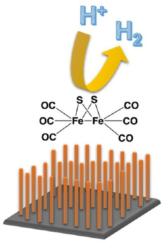
:
1. Introduction
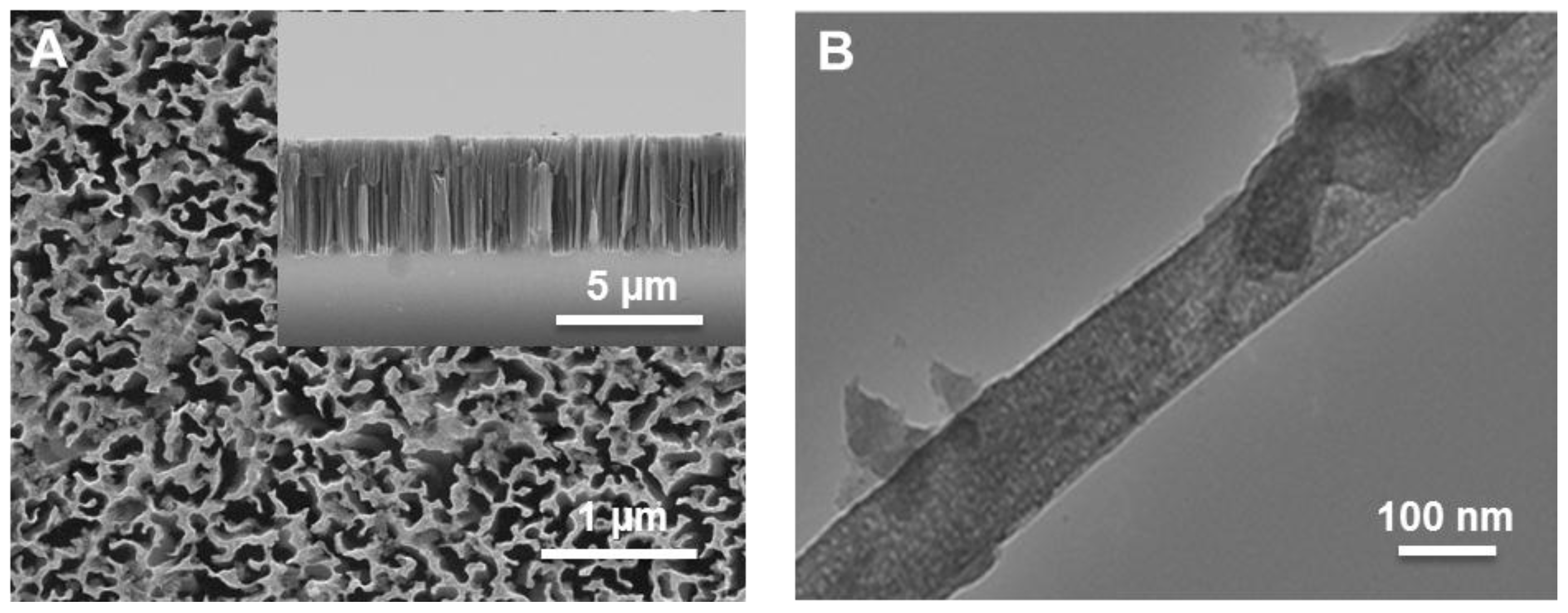
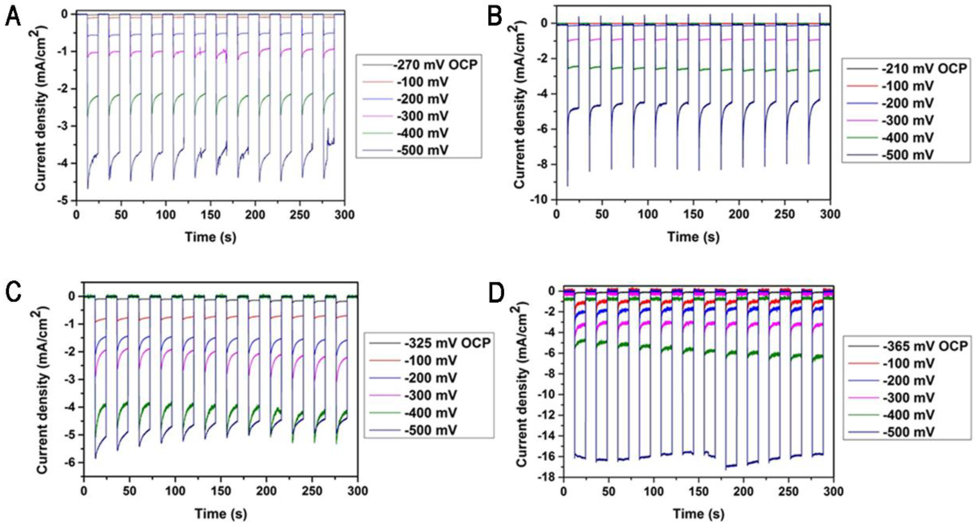
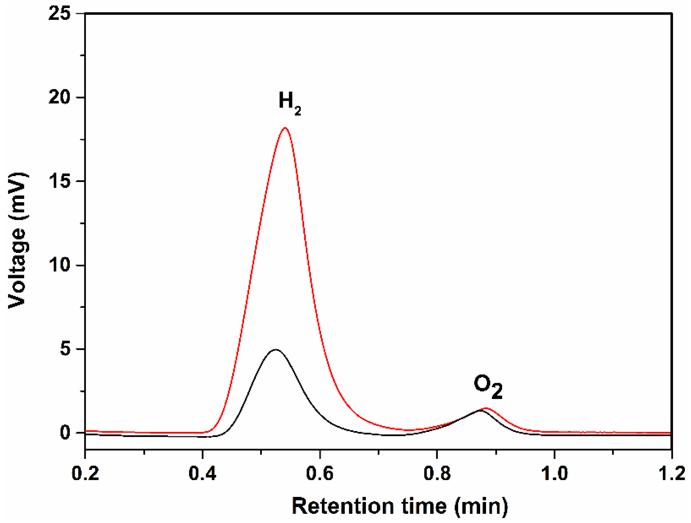
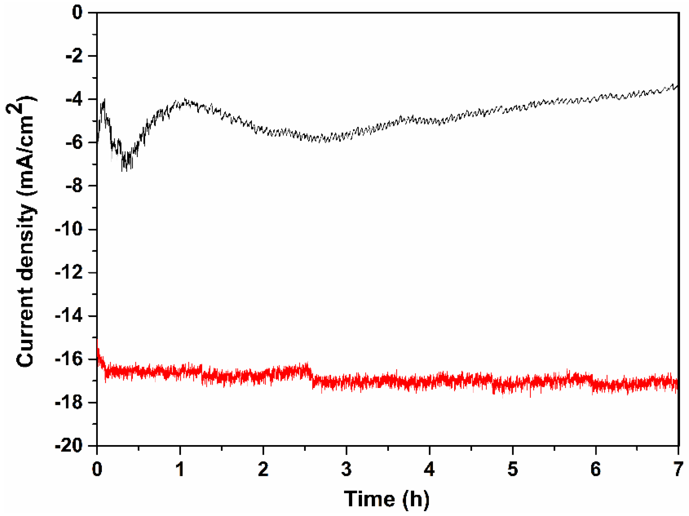
2. Results and Discussion
3. Materials and Methods
3.1. Materials
3.2. SiNW Fabrication
3.3. Electrode Fabrication
3.4. Surface Characterisation
3.5. Photocurrent and GC Measurements
4. Conclusions
Acknowledgments
Author Contributions
Conflicts of Interest
References
- Hisatomi, T.; Kubota, J.; Domen, K. Recent advances in semiconductors for photocatalytic and photoelectrochemical water splitting. Chem. Soc. Rev. 2014, 43, 7520–7535. [Google Scholar] [CrossRef] [PubMed]
- Goetzberger, A.; Hebling, C.; Schock, H.W. Photovoltaic materials, history, status and outlook. Mater. Sci. Eng. R-Rep. 2003, 40, 1–46. [Google Scholar] [CrossRef]
- Navarro, R.M.; Del Valle, F.; de la Mano, J.V.; Álvarez-Galván, M.C.; Fierro, J.L. Photocatalytic water splitting under visible light: Concept and catalysts development. Adv. Chem. Eng. 2009, 36, 111–143. [Google Scholar]
- Sun, K.; Shen, S.; Liang, Y.; Burrows, P.E.; Mao, S.S.; Wang, D. Enabling silicon for solar-fuel production. Chem. Rev. 2014, 114, 8662–8719. [Google Scholar] [CrossRef] [PubMed]
- Chandrasekaran, S.; Nann, T.; Voelcker, N.H. Nanostructured silicon photoelectrodes for solar water electrolysis. Nano Energy 2015, 17, 308–322. [Google Scholar] [CrossRef]
- Oh, I.; Kye, J.; Hwang, S. Fabrication of metal-semiconductor interface in porous silicon and its photoelectrochemical hydrogen production. Bull. Korean Chem. Soc. 2011, 32. [Google Scholar] [CrossRef]
- Chandrasekaran, S.; Macdonald, T.J.; Mange, Y.J.; Voelcker, N.H.; Nann, T. A quantum dot sensitized catalytic porous silicon photocathode. J. Mater. Chem. A 2014, 2, 9478–9481. [Google Scholar] [CrossRef]
- Chandrasekaran, S.; Sweetman, M.J.; Kant, K.; Skinner, W.; Losic, D.; Nann, T.; Voelcker, N.H. Silicon diatom frustules as nanostructured photoelectrodes. Chem. Comm. 2014, 50, 10441–10444. [Google Scholar] [CrossRef] [PubMed]
- Chandrasekaran, S.; McInnes, S.J.; Macdonald, T.J.; Nann, T.; Voelcker, N.H. Porous silicon nanoparticles as a nanophotocathode for photoelectrochemical water splitting. RSC Adv. 2015, 5, 85978–85982. [Google Scholar] [CrossRef]
- Chandrasekaran, S.; Macdonald, T.J.; Gerson, A.R.; Nann, T.; Voelcker, N.H. Boron-Doped Silicon Diatom Frustules as a Photocathode for Water Splitting. ACS Appl. Mater. Interfaces 2015, 7, 17381–17387. [Google Scholar] [CrossRef] [PubMed]
- Oh, I.; Kye, J.; Hwang, S. Enhanced photoelectrochemical hydrogen production from silicon nanowire array photocathode. Nano Lett. 2011, 12, 298–302. [Google Scholar] [CrossRef] [PubMed]
- Peng, K.Q.; Wang, X.; Wu, X.L.; Lee, S.T. Platinum nanoparticle decorated silicon nanowires for efficient solar energy conversion. Nano Lett. 2009, 9, 3704–3709. [Google Scholar] [CrossRef] [PubMed]
- Tran, D.P.; Macdonald, T.J.; Wolfrum, B.; Stockmann, R.; Nann, T.; Offenhäusser, A.; Thierry, B. Photoresponsive properties of ultrathin silicon nanowires. Appl. Phys. Lett. 2014, 105. [Google Scholar] [CrossRef]
- Boettcher, S.W.; Warren, E.L.; Putnam, M.C.; Santori, E.A.; Turner-Evans, D.; Kelzenberg, M.D.; Walter, M.G.; McKone, J.R.; Brunschwig, B.S.; Atwater, H.A.; et al. Photoelectrochemical hydrogen evolution using Si microwire arrays. J. Am. Chem. Soc. 2011, 133, 1216–1219. [Google Scholar] [CrossRef] [PubMed]
- Hasan, M.; Huq, M.F.; Mahmood, Z.H. A review on electronic and optical properties of silicon nanowire and its different growth techniques. Springerplus 2013, 2. [Google Scholar] [CrossRef] [PubMed]
- Hu, L.; Chen, G. Analysis of optical absorption in silicon nanowire arrays for photovoltaic applications. Nano Lett. 2007, 7, 3249–3252. [Google Scholar] [CrossRef] [PubMed]
- Wu, X.; Kulkarni, J.S.; Collins, G.; Petkov, N.; Almécija, D.; Boland, J.J.; Erts, D.; Holmes, J.D. Synthesis and electrical and mechanical properties of silicon and germanium nanowires. Chem. Mater. 2008, 20, 5954–5967. [Google Scholar] [CrossRef]
- Bandaru, P.R.; Pichanusakorn, P. An outline of the synthesis and properties of silicon nanowires. Semicond. Sci. Technol. 2010, 25. [Google Scholar] [CrossRef]
- Yuan, G.D.; Zhou, Y.B.; Guo, C.S.; Zhang, W.J.; Tang, Y.B.; Li, Y.Q.; Chen, Z.H.; He, Z.B.; Zhang, X.J.; Wang, P.F.; et al. Tunable electrical properties of silicon nanowires via surface-ambient chemistry. ACS Nano 2010, 4, 3045–3052. [Google Scholar] [CrossRef] [PubMed]
- Thelander, C.; Agarwal, P.; Brongersma, S.; Eymery, J.; Feiner, L.F.; Forchel, A.; Scheffler, M.; Riess, W.; Ohlsson, B.J.; Gösele, U.; et al. Nanowire-based one-dimensional electronics. Mater. Today 2006, 9, 28–35. [Google Scholar] [CrossRef]
- Filonov, A.B.; Petrov, G.V.; Novikov, V.A.; Borisenko, V.E. Orientation effect in electronic properties of silicon wires. Appl. Phys. Lett. 1995, 67, 1090–1091. [Google Scholar] [CrossRef]
- Schmidt, V.; Wittemann, J.V.; Senz, S.; Gösele, U. Silicon nanowires: A review on aspects of their growth and their electrical properties. Adv. Mater. 2009, 21, 2681–2702. [Google Scholar] [CrossRef]
- Huang, Z.; Geyer, N.; Werner, P.; De Boor, J.; Gösele, U. Metal-assisted chemical etching of silicon: A review. Adv. Mater. 2011, 23, 285–308. [Google Scholar] [CrossRef] [PubMed]
- Zhao, Y.; Anderson, N.C.; Ratzloff, M.W.; Mulder, D.W.; Zhu, K.; Turner, J.A.; Neale, N.R.; King, P.W.; Branz, H.M. Proton reduction using a hydrogenase-modified nanoporous black silicon photoelectrode. ACS Appl. Mater. Interfaces 2016, 8. [Google Scholar] [CrossRef] [PubMed]
- Zhao, Y.; Anderson, N.C.; Zhu, K.; Aguiar, J.A.; Seabold, J.A.; Lagemaat, J.V.; Branz, H.M.; Neale, N.R.; Oh, J. Oxidatively stable nanoporous silicon photocathodes with enhanced onset voltage for photoelectrochemical proton reduction. Nano Lett. 2015, 15, 2517–2525. [Google Scholar] [CrossRef] [PubMed]
- Elnathan, R.; Isa, L.; Brodoceanu, D.; Nelson, A.; Harding, F.J.; Delalat, B.; Kraus, T.; Voelcker, N.H. Versatile particle-based route to engineer vertically aligned silicon nanowire arrays and nanoscale pores. ACS Appl. Mater. Interfaces 2015, 7, 23717–23724. [Google Scholar] [CrossRef] [PubMed]
- Alhmoud, H.Z.; Guinan, T.M.; Elnathan, R.; Kobus, H.; Voelcker, N.H. Surface-assisted laser desorption/ionization mass spectrometry using ordered silicon nanopillar arrays. Analyst 2014, 139, 5999–6009. [Google Scholar] [CrossRef] [PubMed]
- Gordon, R.B.; Bertram, M.; Graedel, T.E. Metal stocks and sustainability. Proc. Natl. Acad. Sci. USA 2006, 103, 1209–1214. [Google Scholar] [CrossRef] [PubMed]
- Kumar, B.; Beyler, M.; Kubiak, C.P.; Ott, S. Photoelectrochemical hydrogen generation by an [FeFe] hydrogenase active site mimic at a p-type silicon/molecular electrocatalyst junction. Chem. Eur. J. 2012, 18, 1295–1298. [Google Scholar] [CrossRef] [PubMed]
- Nann, T.; Ibrahim, S.K.; Woi, P.M.; Xu, S.; Ziegler, J.; Pickett, C.J. Water splitting by visible light: A nanophotocathode for hydrogen production. Angew. Chem. Int. Ed. 2010, 49, 1574–1577. [Google Scholar] [CrossRef] [PubMed]
- Dasgupta, N.P.; Liu, C.; Andrews, S.; Prinz, F.B.; Yang, P. Atomic layer deposition of platinum catalysts on nanowire surfaces for photoelectrochemical water reduction. J. Am. Chem. Soc. 2013, 135, 12932–12935. [Google Scholar] [CrossRef] [PubMed]
- Huang, Z.; Wang, C.; Pan, L.; Tian, F.; Zhang, X.; Zhang, C. Enhanced photoelectrochemical hydrogen production using silicon nanowires@MoS3. Nano Energy 2013, 2, 1337–1346. [Google Scholar] [CrossRef]
- Lee, C.Y.; Park, H.S.; Fontecilla-Camps, J.C.; Reisner, E. Photoelectrochemical H2 evolution with a hydrogenase immobilized on a TiO2-protected silicon electrode. Angew. Chem. Int. Ed. 2016, 55, 5971–5974. [Google Scholar] [CrossRef] [PubMed]
- Zhang, K.; Jing, D.; Xing, C.; Guo, L. Significantly improved photocatalytic hydrogen production activity over Cd1−xZnxS photocatalysts prepared by a novel thermal sulfuration method. Int. J. Hydrog. Energy 2007, 32, 4685–4691. [Google Scholar] [CrossRef]


© 2016 by the authors; licensee MDPI, Basel, Switzerland. This article is an open access article distributed under the terms and conditions of the Creative Commons Attribution (CC-BY) license (http://creativecommons.org/licenses/by/4.0/).
Share and Cite
Chandrasekaran, S.; Nann, T.; Voelcker, N.H. Silicon Nanowire Photocathodes for Photoelectrochemical Hydrogen Production. Nanomaterials 2016, 6, 144. https://doi.org/10.3390/nano6080144
Chandrasekaran S, Nann T, Voelcker NH. Silicon Nanowire Photocathodes for Photoelectrochemical Hydrogen Production. Nanomaterials. 2016; 6(8):144. https://doi.org/10.3390/nano6080144
Chicago/Turabian StyleChandrasekaran, Soundarrajan, Thomas Nann, and Nicolas H. Voelcker. 2016. "Silicon Nanowire Photocathodes for Photoelectrochemical Hydrogen Production" Nanomaterials 6, no. 8: 144. https://doi.org/10.3390/nano6080144
APA StyleChandrasekaran, S., Nann, T., & Voelcker, N. H. (2016). Silicon Nanowire Photocathodes for Photoelectrochemical Hydrogen Production. Nanomaterials, 6(8), 144. https://doi.org/10.3390/nano6080144