Fabrication of Periodic Nanostructures on Silicon Suboxide Films with Plasmonic Near-Field Ablation Induced by Low-Fluence Femtosecond Laser Pulses

 ,
, 
Abstract
:1. Introduction
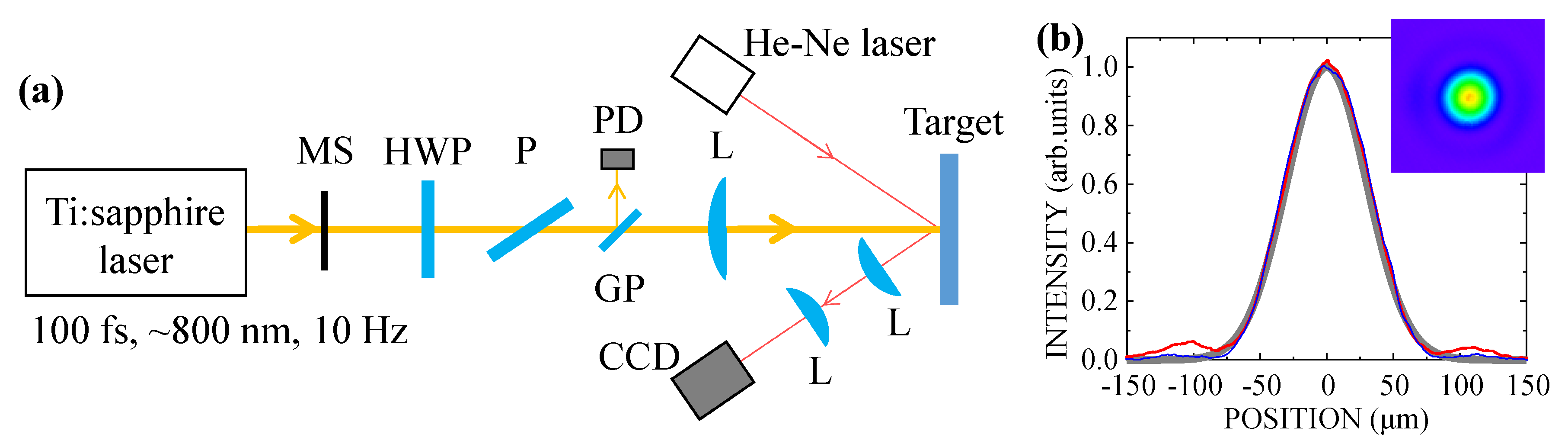
2. Experimental
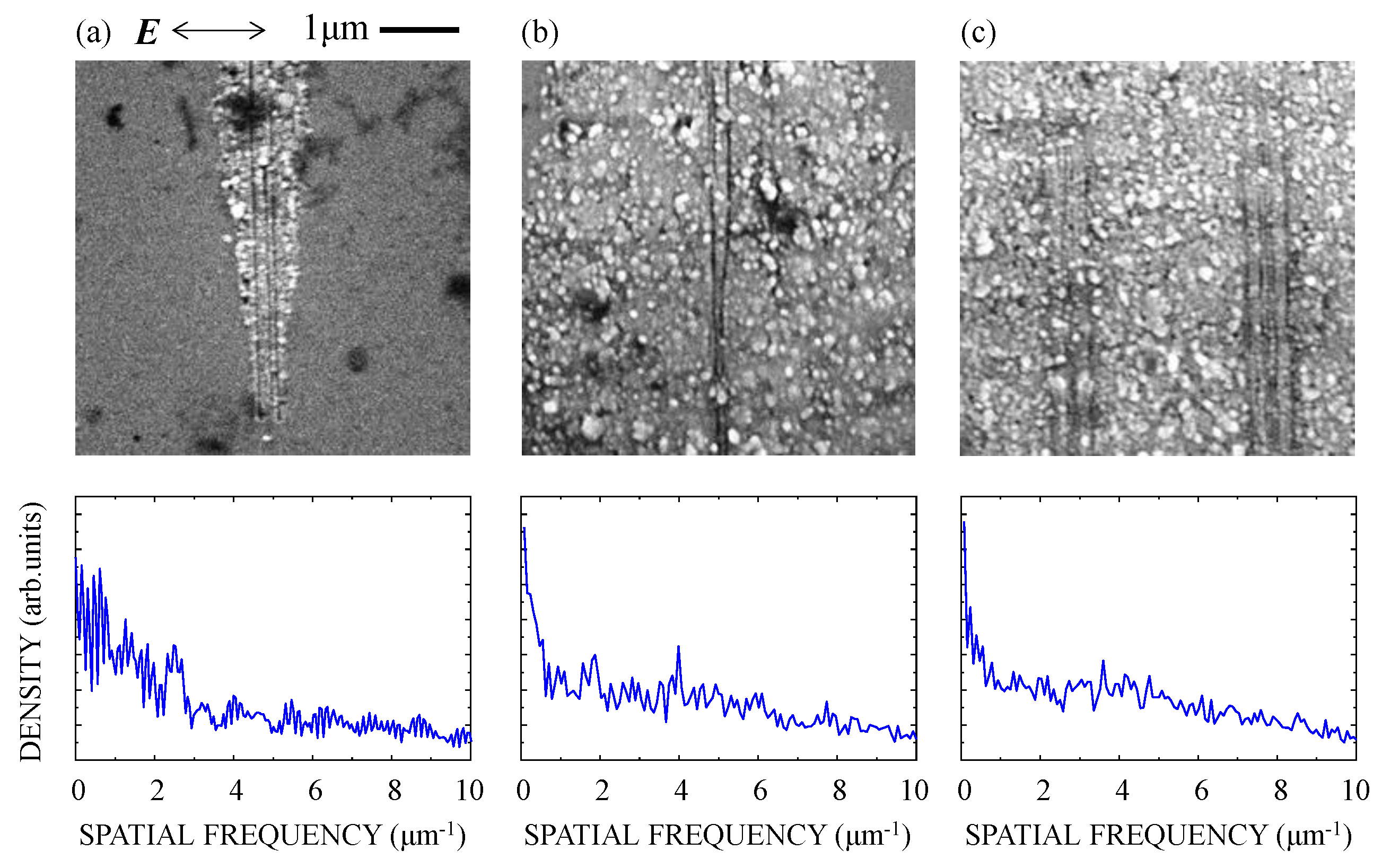
3. Results and Discussion
4. Conclusions
Author Contributions
Funding
Acknowledgments
Conflicts of Interest
References
- Yariv, A.; Yeh, P. Optical Waves in Crystals: Propagation and Control of Laser Radiation; Wiley: New York, NY, USA, 2003; pp. 69–154. [Google Scholar]
- Bohren, C.F.; Huffman, D.R. Absorption and Scattering of Light by Small Particles; Wiley-VCH Verlag: Weinheim, Germany, 1998; pp. 82–129. [Google Scholar]
- Cai, W.; Chettiar, U.K.; Kildishev, A.V.; Shalaev, V.M. Optical cloaking with metamaterials. Nat. Photo. 2007, 1, 224–227. [Google Scholar] [CrossRef] [Green Version]
- Valentine, J.; Li, J.; Zentgraf, T.; Bartal, G.; Zhang, X. An optical cloak made of dielectrics. Nat. Mat. 2009, 8, 568–571. [Google Scholar] [CrossRef] [PubMed] [Green Version]
- Yablonovitch, E. Photonic band-gap structures. J. Opt. Soc. Am. B 1993, 10, 283–295. [Google Scholar] [CrossRef]
- Noda, S.; Chutinan, A.; Imada, M. Trapping and emission of photons by a single defect in a photonic bandgap structure. Nature 2000, 407, 608–610. [Google Scholar] [CrossRef] [PubMed]
- Yu, N.; Genevet, P.; Kats, M.A.; Aieta, F.; Tetienne, J.-P.; Capasso, F.; Gaburro, Z. Light Propagation with Phase Discontinuities: Generalized Laws of Reflection and Refraction. Science 2011, 334, 333–337. [Google Scholar] [CrossRef] [Green Version]
- Yu, N.; Capasso, F. Flat optics with designer metasurfaces. Nat Mater. 2014, 13, 139–150. [Google Scholar] [CrossRef]
- Shimotsuma, Y.; Kazansky, P.G.; Qiu, J.; Hirao, K. Self-Organized Nanogratings in Glass Irradiated by Ultrashort Light Pulses. Phys. Rev. Lett. 2003, 91, 247405. [Google Scholar] [CrossRef] [Green Version]
- Bhardwaj, V.R.; Simova, E.; Rajeev, P.P.; Hnatovsky, C.; Taylor, R.S.; Rayner, D.M.; Corkum, P.B. Optically Produced Arrays of Planar Nanostructures inside Fused Silica. Phys. Rev. Lett. 2006, 96, 057404. [Google Scholar] [CrossRef]
- Wagner, R.; Gottmann, J.; Horn, A.; Kreutz, E.W. Subwavelength ripple formation induced by tightly focused femtosecond laser radiation. Appl. Surf. Sci. 2006, 252, 8576–8579. [Google Scholar] [CrossRef]
- Beresna, M.; Gecevičius, M.; Kazansky, P.G.; Gertus, T. Radially polarized optical vortex converter created by femtosecond laser nanostructuring of glass. Appl. Phys. Lett. 2011, 98, 201101. [Google Scholar] [CrossRef]
- Ion, J.C. Laser Processing of Engineering Materials; Elsevier Butterworth-Heinemann: Oxford, UK, 2005; pp. 104–138. [Google Scholar]
- Kannatey-Asibu, E., Jr. Principles of Laser Materials Processing; John Wiley & Sons: Hoboken, NJ, USA, 2008; pp. 409–430. [Google Scholar]
- Phillip, H.R. Optical properties of non-crystalline Si, SiO, SiOx and SiO2. J. Phys. Chem. Solids 1971, 32, 1935–1945. [Google Scholar] [CrossRef]
- Hernández, S.; Pellegrino, P.; Martínez, A.; Lebour, Y.; Garrido, B.; Spano, R.; Cazzanelli, M.; Daldosso, N.; Pavesi, L.; Jordana, E.; et al. Linear and nonlinear optical properties of Si nanocrystals in SiO2 deposited by plasma-enhanced chemical-vapor deposition. J. Appl. Phys. 2008, 103, 064309. [Google Scholar] [CrossRef] [Green Version]
- Minissale, S.; Yerci, S.; Dal Negro, L. Nonlinear optical properties of low temperature annealed silicon-rich oxide and silicon-rich nitride materials for silicon photonics. Appl. Phys. Lett. 2012, 100, 021109. [Google Scholar] [CrossRef]
- Fricke-Begemann, T.; Meinertz, J.; Weichenhain-Schriever, R.; Ihlemann, J. Silicon suboxide (SiOx): Laser processing and applications. Appl. Phys. A Mater. Sci. Process. 2014, 117, 13–18. [Google Scholar] [CrossRef]
- Kahler, U.; Hofmeister, H. Size evolution and photoluminescence of silicon nanocrystallites in evaporated SiOx thin films upon thermal processing. Appl. Phys. A 2002, 74, 13–17. [Google Scholar] [CrossRef]
- Friz, M.; Waibel, F. Coating Material. In Optical Interference Coatings; Kaiser, N., Pulker, H.K., Eds.; Springer-Verlag: Berlin, Germany, 2003; pp. 105–130. [Google Scholar]
- Roschuk, T.; Li, J.; Wojcik, J.; Mascher, P.; Calder, I.D. Lighting Applications of Rare Earth-Doped Silicon Oxides. In Silicon Nanocrystals: Fundamentals, Synthesis and Applications; Pavesi, L., Turan, R., Eds.; Wiley-VCH Verlag: Weinheim, Germany, 2010; pp. 487–506. [Google Scholar]
- Sirleto, L.; Ferrara, M.A.; Nikitin, T.; Novikov, S.; Khriachtchev, L. Giant Raman gain in silicon nanocrystals. Nat. Commun. 2012, 3, 1220. [Google Scholar] [CrossRef] [Green Version]
- Schulz-Ruhtenberg, M.; Ihlemann, J.; Heber, J. Laser patterning of SiOx-layers for the fabrication of UV diffractive phase elements. Appl. Surf. Sci. 2005, 248, 190–195. [Google Scholar] [CrossRef]
- Takaya, T.; Miyaji, G.; Richter, L.J. Ihlemann, Nanostructure Formation on Silicon Suboxide with Plasmonic Near-Field Ablation Induced by Femtosecond Laser Pulses. In Proceedings of the 2019 Conference on Lasers and Electro-Optics Europe & European Quantum Electronics Conference (CLEO/Europe-EQEC), Munich, Germany, 23–27 June 2019. [Google Scholar]
- Miyazaki, K.; Miyaji, G. Mechanism and control of periodic surface nanostructure formation with femtosecond laser pulses. Appl. Phys. A 2014, 114, 177–185. [Google Scholar] [CrossRef] [Green Version]
- Gamaly, E.G.; Juodkazis, S.; Nishimura, K.; Misawa, H.; Luther-Davies, B.; Hallo, L.; Nicolai, P.; Tikhonchuk, V.T. Laser-matter interaction in the bulk of a transparent solid: Confined microexplosion and void formation. Phys. Rev. B-Condens. Matter Mater. Phys. 2006, 73, 1–15. [Google Scholar] [CrossRef]
- Gräf, S.; Kunz, C.; Müller, F.A. Formation and Properties of Laser-Induced Periodic Surface Structures on 254 Different Glasses. Materials 2017, 10, 933. [Google Scholar] [CrossRef] [Green Version]
- Juodkazis, S.; Nishi, Y.; Misawa, H.; Mizeikis, V.; Schecker, O.; Waitz, R.; Leiderer, P.; Scheer, E. Optical transmission and laser structuring of silicon membranes. Opt. Express 2009, 15308–15317. [Google Scholar] [CrossRef] [PubMed]
- Bonse, J.; Rudolph, P.; Krüger, J.; Baudach, S.; Kautek, W. Femtosecond pulse laser processing of TiN on silicon. Appl. Surf. Sci. 2000, 154, 659–663. [Google Scholar] [CrossRef]
- Yasumaru, N.; Miyazaki, K.; Kiuchi, J. Glassy carbon layer formed in diamond-like carbon films with femtosecond laser pulses. Appl. Phys. A 2004, 79, 425–427. [Google Scholar] [CrossRef]
- Žemaitis, A.; Gaidys, M.; Brikas, M.; Gečys, P.; Račiukaitis, G.; Gedvilas, M. Advanced laser scanning for highly-efficient ablation and ultrafast surface structuring: Experiment and model. Sci. Rep. 2018, 8, 1–14. [Google Scholar] [CrossRef]
- Miyaji, G.; Miyazaki, K. Origin of periodicity in nanostructuring on thin film surfaces ablated with femtosecond laser pulses. Opt. Express 2008, 16, 16265–16271. [Google Scholar] [CrossRef] [PubMed]
- Miyaji, G.; Miyazaki, K.; Zhang, K.; Yoshifuji, T.; Fujita, J. Mechanism of femtosecond-laser-induced periodic nanostructure formation on crystalline silicon surface immersed in water. Opt. Express 2012, 20, 14848–14856. [Google Scholar] [CrossRef] [PubMed]
- Puerto, D.; Gawelda, W.; Siegel, J.; Bonse, J.; Bachelier, G.; Solis, J. Transient reflectivity and transmission changes during plasma formation and ablation in fused silica induced by femtosecond laser pulses. Appl. Phys. A 2008, 92, 803–808. [Google Scholar] [CrossRef] [Green Version]
- Ibach, H.; Lüth, H. Solid-State Physics, An Introduction to Principles of Materials Science, 4th ed.; Springer: Berlin/Heidelberg, Germany, 2009; pp. 371–403. [Google Scholar]
- Wang, S. Solid-State Electronics; McGraw-Hill: New York, NY, USA, 1966; pp. 262–308. [Google Scholar]
- Shah, J.; Leheny, R.F.; Lin, C. Dynamic Burstein shift in GaAs. Solid State Commun. 1976, 18, 1035–1037. [Google Scholar] [CrossRef]
- Oudar, J.L.; Hulin, D.; Migus, A.; Antonetti, A.; Alexandre, F. Subpicosecond spectral hole burning due to nonthermalized photoexcited carriers in GaAs. Phys. Rev. Lett. 1985, 55, 2074–2077. [Google Scholar] [CrossRef]
- Wolff, P.A. Theory of the Band Structure of Very Degenerate Semiconductors. Phys. Rev. 1962, 126, 405–412. [Google Scholar] [CrossRef]
- Berggren, K.-F.; Sernelius, B.E. Band-gap narrowing in heavily doped many-valley semiconductors. Phys. Rev. B 1981, 24, 1971–1986. [Google Scholar] [CrossRef]
- Abram, R.A.; Childs, G.N.; Saunderson, P.A. Band gap narrowing due to many-body effects in silicon and gallium arsenide. J. Phys. C 1984, 17, 6105–6125. [Google Scholar] [CrossRef]
- Raether, H. Surface Plasmons on Smooth and Rough Surfaces and on Gratings; Springer-Verlag: Heidelberg, Germany, 1988; pp. 4–7. [Google Scholar]
- Sipe, J.E.; Young, J.F.; Preston, J.S.; Van Driel, H.M. Laser-induced periodic surface structure. I. Theory. Phys. Rev. B 1983, 27, 1141–1154. [Google Scholar] [CrossRef]
- Bonse, J.; Rosenfeld, A.; Krüger, J. On the role of surface plasmon polaritons in the formation of laser-induced periodic surface structures upon irradiation of silicon by femtosecond-laser pulses. J. Appl. Phys. 2009, 106, 104910. [Google Scholar] [CrossRef]
- Garrelie, F.; Colombier, J.-P.; Pigeon, F.; Tonchev, S.; Faure, N.; Bounhalli, M.; Reynaud, S.; Parriaux, O. Evidence of surface plasmon resonance in ultrafast laser-induced ripples. Opt. Express 2011, 19, 9035–9043. [Google Scholar] [CrossRef]
- Novotny, L.; Hecht, B.; Pohl, D.W. Interference of locally excited surface plasmons. J. Appl. Phys. 1997, 81, 1798–1806. [Google Scholar] [CrossRef]
- Liu, Z.; Wei, Q.; Zhang, X. Surface Plasmon Interference Nanolithography. Nano Lett. 2005, 5, 957–961. [Google Scholar] [CrossRef]
- Vorobyev, A.Y.; Guo, C. Direct femtosecond laser surface nano/microstructuring and its applications. Laser Photonics Rev. 2013, 7, 385–407. [Google Scholar] [CrossRef]
- Buividas, R.; Mikutis, M.; Juodkazis, S. Surface and bulk structuring of materials by ripples with long and short laser pulses: Recent advances. Prog. Quantum Electron. 2014, 38, 119–156. [Google Scholar] [CrossRef]
- Stankevič, V.; Račiukaitis, G.; Bragheri, F.; Wang, X.; Gamaly, E.G.; Osellame, R.; Juodkazis, S. Laser printed nano-gratings: Orientation and period peculiarities. Sci. Rep. 2017, 7, 1–8. [Google Scholar] [CrossRef] [Green Version]
- Wang, L.; Chen, Q.-D.; Cao, X.-W.; Buividas, R.; Wang, X.; Juodkazis, S.; Sun, H.-B. Plasmonic nano-printing: Large-area nanoscale energy deposition for efficient surface texturing. Light Sci. Appl. 2017, 6, e17112. [Google Scholar] [CrossRef] [PubMed]
- Arnold, D.; Cartier, E.; Dimaria, D.J. Acoustic-phonon runaway and impact ionization by hot electrons in silicon dioxide. Phys. Rev. B 1992, 45, 1477–1480. [Google Scholar] [CrossRef]
- Sun, Q.; Jiang, H.; Liu, Y.; Wu, Z.; Yang, H.; Gong, Q. Measurement of the collision time of dense electronic plasma induced by a femtosecond laser in fused silica. Opt. Lett. 2005, 30, 320. [Google Scholar] [CrossRef]
- Shank, C.V.; Yen, R.; Hirlimann, C. Time-resolved reflectivity measurements of femtosecond-optical-pulse- induced phase transitions in silicon. Phys. Rev. Lett. 1983, 454–457. [Google Scholar] [CrossRef]
- Voisiat, B.; Gedvilas, M.; Indrišiunas, S.; Raciukaitis, G. Flexible microstructuring of thin films using multi-beam interference: Ablation with ultrashort lasers. J. Laser Micro Nanoeng. 2011, 6, 185–190. [Google Scholar] [CrossRef]


© 2020 by the authors. Licensee MDPI, Basel, Switzerland. This article is an open access article distributed under the terms and conditions of the Creative Commons Attribution (CC BY) license (http://creativecommons.org/licenses/by/4.0/).
Share and Cite
Takaya, T.; Miyaji, G.; Takahashi, I.; Richter, L.J.; Ihlemann, J. Fabrication of Periodic Nanostructures on Silicon Suboxide Films with Plasmonic Near-Field Ablation Induced by Low-Fluence Femtosecond Laser Pulses. Nanomaterials 2020, 10, 1495. https://doi.org/10.3390/nano10081495
Takaya T, Miyaji G, Takahashi I, Richter LJ, Ihlemann J. Fabrication of Periodic Nanostructures on Silicon Suboxide Films with Plasmonic Near-Field Ablation Induced by Low-Fluence Femtosecond Laser Pulses. Nanomaterials. 2020; 10(8):1495. https://doi.org/10.3390/nano10081495
Chicago/Turabian StyleTakaya, Tatsuyoshi, Godai Miyaji, Issei Takahashi, Lukas Janos Richter, and Jürgen Ihlemann. 2020. "Fabrication of Periodic Nanostructures on Silicon Suboxide Films with Plasmonic Near-Field Ablation Induced by Low-Fluence Femtosecond Laser Pulses" Nanomaterials 10, no. 8: 1495. https://doi.org/10.3390/nano10081495