Article

Mitigating the Impact of Mask Absorber Error on Lithographic Performance by Lithography System Holistic Optimization

Key Laboratory of Photoelectronic Imaging Technology and System of Ministry of Education of China, School of Optics and Photonics, Beijing Institute of Technology, Beijing 100081, China
*
Author to whom correspondence should be addressed.
Appl. Sci. 2019, 9(7), 1275; https://doi.org/10.3390/app9071275
Submission received: 5 March 2019 / Revised: 19 March 2019 / Accepted: 22 March 2019 / Published: 27 March 2019

Abstract

:
The non-ideal mask absorber can cause an increase in critical dimension error (CDE) and decrease in process window (PW). However, the random mask absorber errors induced during mask fabricating and measuring are not considered in computational lithography. The problem cannot be neglected as the continuous scaling of lithography technology node. In this work, for the first time to our knowledge, a source, numerical aperture (NA), and process parameters co-optimization (SNPCO) method is developed to reduce the CDE induced by absorber errors and improve the PW. First, the source is represented by Zernike polynomials to balance computational burden and flexibility of source. Then a weighted cost function containing CDE and PW that incorporates the influences of absorber errors is created. Finally, a statistical optimization method is used to optimize the lithographic system parameters. Simulations of 1D mask pattern show that for the system with extreme absorber errors, the pattern errors of the proposed method are reduced by 62.1% and 58.9%, and the PWs are increased by 40.3% and 36.4%, respectively. The results illustrate that this method is effective in mitigating the CDE caused absorber errors and improving process robustness.

1. Introduction

With the continuous scaling in the feature size of lithography technology node, the deep ultraviolet (DUV) lithography steps into the ultra-low k 1 regime [1]. As the feature’s sizes on a mask are smaller than the scanner exposure wavelength, the 3D mask effects must be taken into account in computational lithography [2,3]. The 3D mask effects are mainly subject to the morphology of the mask absorber including mask absorber thickness and absorber profile. Related research has indicated that mask absorber thickness (MAT) and the absorber sidewall angle (SWA) have a big impact on critical dimension (CD), best focus (BF), and depth of focus (DOF) [4,5,6,7,8,9]. However, mask absorber errors are inevitably introduced by the imperfect etching process in mask fabrication and measurement [10,11]. In addition, the MAT error and tapered SWA deformation of the absorber are increased by repeated mask cleaning process [12,13]. Recently, Sturtevant et al. and Rudolph et al. studied the impact of photomask uncertainties on computational lithography [4,14,15]. The results revealed that the variations of MAT and SWA cause significant CD errors (CDEs) that cannot be ignored. The research of Wisdom et al. [16] and Ko et al. [17] indicated that the SWA variations of the mask absorber also have great influence on the lithography patterning result. Therefore, it is very necessary to mitigate the impacts of mask absorber errors on lithography performance in computational lithography.
Various advanced computational lithography techniques have been proposed to compensate for the 3D mask effects. Sears et al. proposed a genetic algorithm-based pupil wavefront optimization (PWO) method to compensate for the wavefront phase error introduced by the mask topography effects [18]. Fühner et al. developed a combined source, mask, and projector pupil optimization (SMPO) procedure to maximize the common process window (PW) [19]. Li et al. presented a conjugate gradient method-based source mask optimization (SMO) approach incorporating pupil wavefront aberrations to improve the usable DOF by compensating for mask topography effects [20]. Han et al. developed an inverse PWO method to improve image fidelity by compensating for thick mask induced aberration including 37 Zernike terms [21]. However, the computational lithography techniques mentioned above are established for an ideal lithography system without taking into account of the impacts of random mask absorber errors on lithography imaging performance.
To mitigate the impact of mask absorber errors on lithographic imaging performance, this paper develops a source, numerical aperture (NA), process parameters co-optimization (SNPCO) method for the DUV lithography system. To achieve this, an effective alternate optimization procedure based on a statistical method is built, which treats the mask absorber errors as random variables and takes their statistical properties into account. In our prior work, we had proposed a mask, process, and lithography-tool parameters co-optimization (MPLCO) method to improve the PW [22]. However, that method adopted a parametric source represented by only three parameters (including inner radius, outer radius, and opening angle) with limited flexibility, and it was established with a 2D mask model without considering the impacts of random mask absorber error on lithography performance. To solve this problem, we first use the Zernike polynomials to represent the source patterns in view of their capacity in fitting arbitrary form wavefront [23,24,25]. The even, symmetric Zernike polynomials are selected as the basis functions based on the symmetry of the DUV lithography illumination source. Thus, a freeform source is created by the linear superposition of these basis functions. In this way, the flexibility of the source pattern is improved, and the computational burden of a pixelated source along with the 3D mask model is avoided. Then, for source optimization, a weighted cost function, which is the superposition of the CDE and normalized image log slopes (NILS) incorporating the impacts of random MAT errors and SWA variations, is innovated to improve image fidelity and process stability. The stochastic gradient (SGD) algorithm is applied to optimize the source. Next, to further increase the PW, the cost function for the NA and process parameters optimization is the DOF at a specific exposure latitude (EL). As these parameters are not of the same order of magnitude, the large-scale parameters are likely to be obstructed by small-scale parameters during the optimization procedure. We employ the normalized stochastic gradient (NSGD) algorithm to optimize the NA and process parameters. Finally, in consideration of the interaction of source, NA, and process parameters on lithography performance, the optimization procedures are implemented alternately to get better performance. The SNPCO method is tested on two types of layouts at 14 nm technology node. Simulations of 1D mask pattern demonstrate that for the system with extreme mask absorber errors, the CDEs of the proposed method are reduced by 62.1% and 58.9%, respectively. In such cases, the corresponding DOFs at EL = 5% are increased by 40.3% and 36.4%, respectively. The results indicate that the proposed method mitigates the CDEs caused by mask absorber errors and improves the process robustness effectively in the DUV lithography system.
The remainder of the paper is organized as follows. In Section 2, the source pattern representation, weighted cost function definition, and inverse optimization problem formulation are described. In Section 3, the gradient-based inverse DUV lithography optimization algorithm is developed. Simulation results are presented in Section 4. Finally, conclusions are provided in Section 5.

2. Modeling of DUV Lithography

It is known that source pattern representation and cost function play an important role in computational lithography. To balance the computational burden and flexibility in the optimization procedure, we need to create a suitable freeform source to minimize the CDE caused by the random mask absorber errors and increase the PW. In addition, we build an effective weighted cost function that incorporates the impacts of the absorber errors.

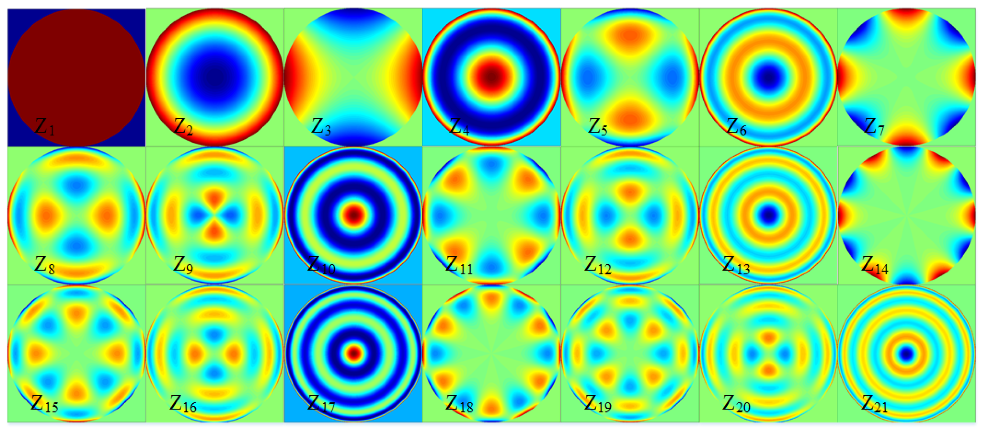
2.1. Source Pattern Representation

For DUV lithography partially coherent imaging systems, the source pattern is limited to a unit circle. In view of the ability of Zernike polynomials in fitting the wavefront of projection objective, we use the Zernike polynomials to represent the source pattern whose form is similar to the wavefront. For ease of calculation, we use a normalized source. Thus, the source pattern is
0 s ( f , g ) 1 , f 2 + g 2 1
where f and g are space frequency coordinates, and s ( f , g ) represents the source pattern.
According to the above constraints, the source pattern is expressed as
s ( f , g ) = T { i = 1 n c i Z i ( f , g ) } ,
where Z i ( f , g ) is the i th Zernike polynomial, c i is its corresponding coefficient, and T { } is an operator to keep the source intensity to meet the requirements of Equation (1). Thus, we set the operator to
T { x } = 1 + cos ( x ) 2 , .
We denote the Zernike coefficients c i as a coefficient vector c:
c = [ c 1 , c 2 , , c n ] , .
Thus, a freeform source pattern can be obtained by changing the Zernike coefficient vector c.
To obtain a symmetric source, we select some suitable, even symmetric Zernike polynomials as the basis functions. The well-chosen 21 basis functions selected from the Zernike polynomials to represent the source pattern are presented in Figure 1.

2.2. Mathematical Modeling

To mitigate the impacts of mask absorber errors and increase the PW, an alternate optimization framework of the source, NA, and process parameters are built to improve the optimization performance. Consequently, we develop different cost functions for the alternate optimization procedure. We evaluate the lithographic imaging performance by measuring both the image fidelity and the process robustness.
The cost function for source optimization consists of two parts: the CDE for the lithography system with random MAT error and SWA error to evaluate the image fidelity, and NILS to improve the PW. Thus, the weighted cost function is formulated as
F S = ε { α 1 P C D E ( c ; M A T , S W A ) α 2 P N I L S ( c ; M A T , S W A ) } ,
where ε { } is the expectation operator to the random absorber errors including the MAT and SWA error which follow the Gaussian distribution; P C D E ( c ; M A T , S W A ) and P N I L S ( c ; M A T , S W A ) represent the absolute value of resist image CDE and aerial image NILS with random mask MAT and SWA error, respectively; α 1 and α 2 are the corresponding weighting coefficients; M A T and S W A represent the value of mask absorber thickness error and absorber sidewall angle error, respectively.
To lighten the computation burden, we calculate F S by discretizing M A T and S W A to a set of values M A T i and S W A j with corresponding probabilities ξ i and η j , that is,
F S = i j ξ i η j { α 1 P C D E ( c ; M A T i , S W A j ) α 2 P N I L S ( c ; M A T i , S W A j ) } , .
Then we denote the NA and process parameter to be optimized as vector x:
x = [ x 1 , x 2 , , x n ] , .
The cost function for NA and process parameters optimization consists of the DOF at a specific exposure latitude (EL) with random MAT and SWA errors to further increase the PW. Thus, the cost function is formulated as
F N P = ε { P D O F ( x ; M A T , S W A ) } ,
where P D O F ( x ; M A T , S W A ) represents the absolute value of the DOF with random MAT and SWA error.
Similarly, the F N P is calculated by discretizing M A T and S W A to a set of values M A T i and S W A j with the corresponding probabilities ξ i and η j , that is,
F N P = i j ξ i η j P D O F ( x ; M A T i , S W A j ) , .
Therefore, the source optimization problem is formulated as searching for the coefficient vector c to minimize the cost function F S . It can be expressed as
c ^ = arg min F S ( c ) ,
where c ^ is the optimum result of c.
The NA and process parameters optimization problem is formulated as seeking the parameter vector x to minimize the cost function F N P . This can be expressed as
x ^ = arg min F N P ( x ) ,
where x ^ is the optimum result of x.

3. SNPCO Method for DUV Lithography System

In this section, we develop a gradient-based SNPCO method to comprehensively optimize the source, NA, and process parameters for mitigating the impacts of mask absorber errors on lithographic imaging performance. For the statistical optimization problem described in Equations (10) and (11), the SGD algorithm is adept in solving such problem [26,27]. Thus, we use the SGD algorithm to optimize the source. And the NSGD algorithm is applied to optimize the NA and process parameters of different scales to improve convergence of algorithm. The optimization procedures are carried out alternately.
The pseudocode in Table 1 explains the procedure of the SNPCO method, and the supplementary explanations are detailed in the following context.
As the NA and process parameters are not of the same order of magnitude, the large-scale parameters are likely to be obstructed by small-scale parameters in the optimization. Hence, we normalize the different scale process parameters in the same range of 0 to 1. The normalization is expressed as
x ¯ = x x min x max x min ,
where parameter vector x min and x max are the minimum and maximum values of x.
Since the SGD method is applied to optimize source, we need to calculate the search direction at the k t h Zernike coefficients iteration point. The search direction is
d S ( k ) = F S ( c ( k ) ) , .
The NSGD method is used to optimize the NA and process parameters. The search direction at the k t h optimization parameters iteration point is
d N P ( k ) = F N P ( x ¯ ( k ) ) , .
As the optimization of lithography process parameters and mask topography effects are involved, there are no explicit analytical relations between the cost function and the optimization parameters. We use a numerical approximation of the gradient instead of calculating the derivative of the cost function.
The gradient of Zernike coefficients vector is expressed as
F S ( c ( k ) ) = F S ( c ( k ) ) F S ( c ( k ) c ) c , .
The gradient of normalized NA and process parameters vector is expressed as
F N P ( x ¯ ( k ) ) = F N P ( x ¯ ( k ) ) F N P ( x ¯ ( k ) x ¯ ) x ¯ ,
where c and x ¯ are the small increments between the current iteration point and its neighboring point.

4. Optimization Results

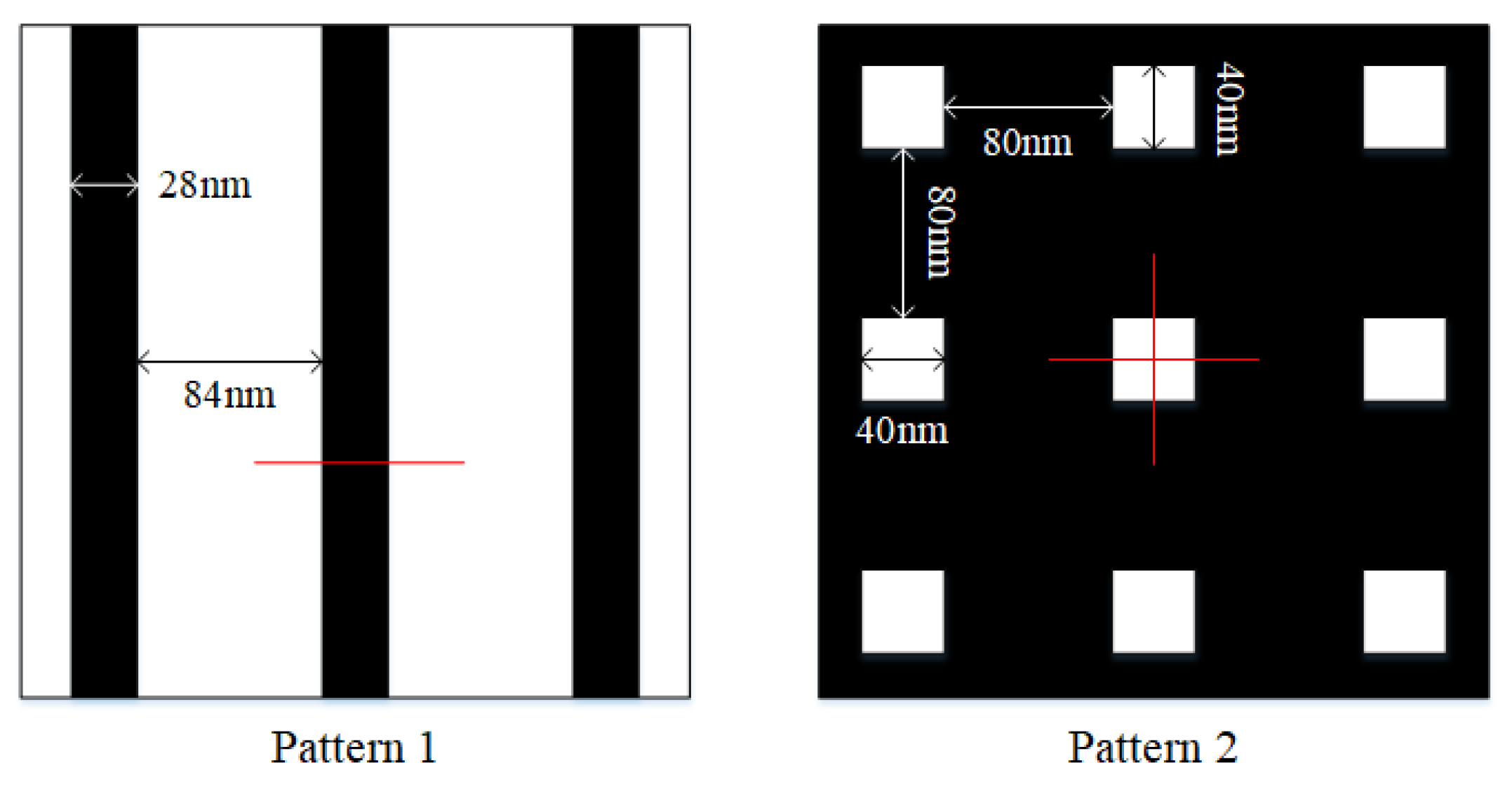
4.1. Simulation Conditions

PROLITH X6.0 software is used to evaluate the lithography imaging performance. A water immersion lithography system with a reduction ratio R = 4 is used. The wavelength is set to 193.368 nm. The illumination is Y-polarized for the line-space mask pattern and TE-polarized for the contact hole mask pattern. The mask absorber of the line-space mask is composed of molybdenum silicide layer (refractive index = 2.343, extinction coefficient = −0.586), and the mask absorber of the contact hole mask is chrome (refractive index = 0.844, extinction coefficient = −1.654). The rigorous coupled wave analysis (RCWA) method is used to calculate the mask diffraction spectrum. The well-calibrated JSR ARX2895JN photoresist is used. Dual bottom antireflective coatings (BARCs) are applied to reduce the substrate reflectivity. The thicknesses of BARCs are 33 nm and 43 nm for the line-space pattern and 24 nm and 43 nm for the contact hole pattern.
A full physical photoresist model and 3-stage post exposure bake (PEB) model are used to simulate the process conditions accurately. The full physical photoresist model is capable of simulating the reaction and diffusion of a chemically amplified photoresist accurately. The 3-stage PEB model describes the temperature variation when the wafer is placed on a hotplate or chill plate and the wafer transition time between the two plates. Four process parameters are selected for optimization, including hotplate duration, transition duration, chill plate duration, and photoresist development time. The NA of the imaging system is chosen for optimization. To ensure the values of these parameters are realizable in lithography, these parameters are set in reasonable ranges. The minimum value and the maximum value are listed in Table 2.
The weighting coefficients α 1 and α 2 in the cost function Equation (6) are set to 0.5 and 0.5, respectively.

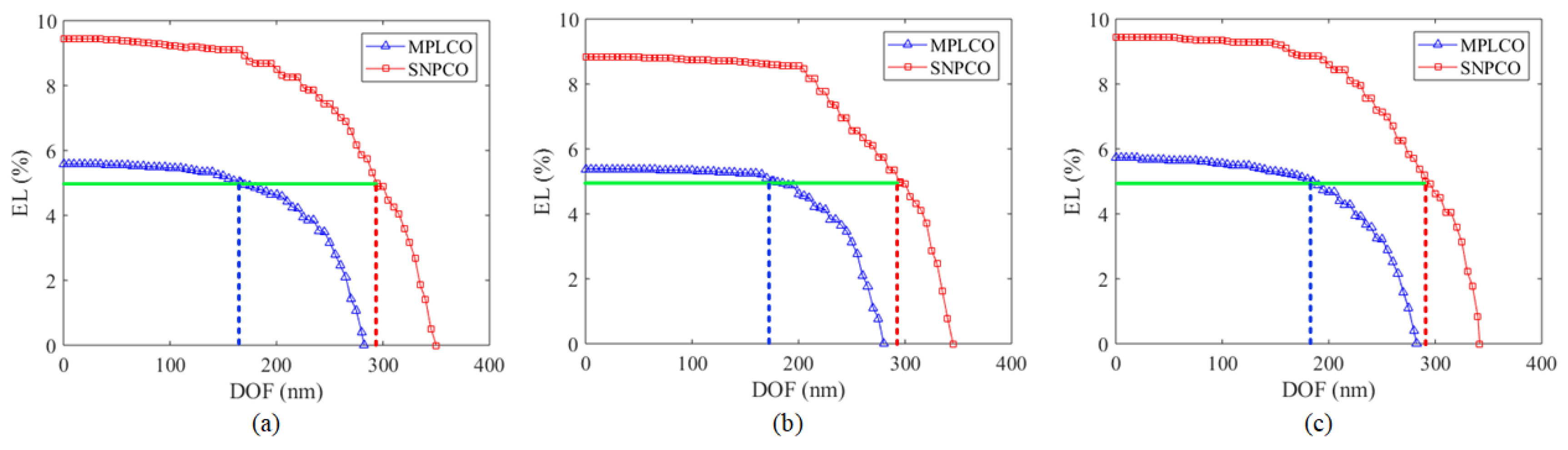
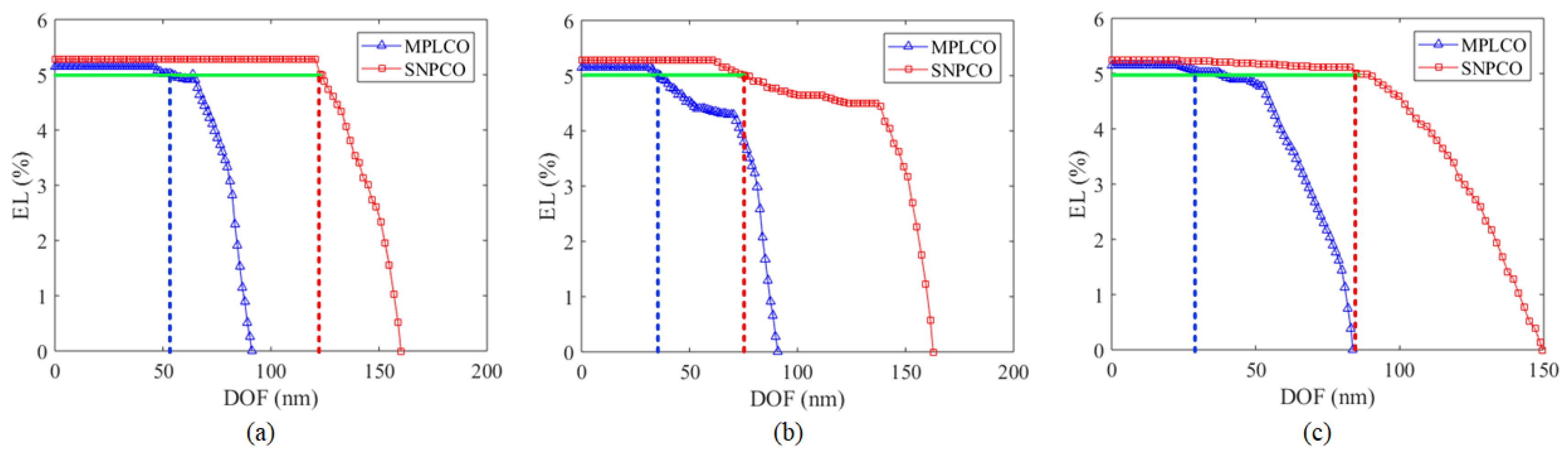
4.2. Simulation Results

This section demonstrates the simulations of the proposed SNPCO method with two types of test patterns at 14 nm technology node. The two types of test patterns are shown in Figure 2, the 1D line space pattern with target CD = 28 nm is referred to as “Pattern 1”, and the 2D contact hole pattern with target CD = 40 nm is referred to as “Pattern 2”, respectively [28,29]. We evaluate the lithographic performance by measuring both the image fidelity and the robustness of process. The image fidelity is evaluated by computing the absolute value of CDE caused by a random mask absorber error. The robustness of process is evaluated by simulating the common PW at critical locations marked by the red lines of the test patterns, and all the measurements are in wafer dimensions.

4.2.1. Line Space Pattern

The validity of the proposed SNPCO method is first demonstrated for pattern 1. The ideal MAT is 68 nm and the ideal SWA is 90°. Figure 3 presents the simulation results of the MPLCO and the SNPCO in the case of pattern 1. From top to bottom, Figure 3 shows the corresponding simulation results of the MPLCO and the SNPCO. From left to right, Figure 3 exhibits the optimized source patterns, mask patterns, resist profiles for the ideal system, and the system with MAT = 63 nm and SWA = 95°. The corresponding NA and process parameters optimization results are listed in Table 3. From the comparison results, it can be seen that the optimized SNPCO source is obviously different from the MPLCO source. The PEB durations, development time, and NA of the SNPCO are all smaller than that of the MPLCO. For the ideal system, the CDEs of the two methods are −0.04 nm and 0.01 nm, respectively. In this case, the image fidelities of the two methods are very close. However, for the system with the MAT = 63 nm, the CDEs of the two cases are −3.43 nm and −1.30 nm. In this case, the CDEs of the SNPCO is 62.1% smaller than that of the MPLCO. For the system with the SWA = 95°, the CDEs of the two cases are 5.35 nm and 2.20 nm. In such circumstance, the CDEs of the SNPCO is 58.9% lower than that of the MPLCO.
Figure 4 shows the exposure latitude (EL) versus DOF curves of the MPLCO and the SNPCO method. Figure 4a–c are the EL versus DOF curves for the ideal system, the system with MAT = 63 nm, and the system with SWA = 95°, respectively. We use the dashed lines to indicate the DOF at EL = 5% in the figure. For the ideal system, the DOFs at EL = 5% of the MPLCO and SNPCO methods are 166 nm and 294 nm, respectively. The DOF of the proposed SNPCO method is 43.5% larger than that of the MPLCO. For the system with MAT = 63 nm, the DOFs at EL = 5% of the MPLCO and SNPCO are 176 nm and 295 nm. In this case, the DOF of the SNPCO is 40.3% larger than that of the MPLCO, and for the system with SWA = 95°, the DOFs at EL = 5% of the MPLCO and SNPCO are 185 nm and 291 nm, respectively. In such circumstance, the DOF of the proposed method is 36.4% larger than that of the MPLCO.
Figure 5 illustrates the mask absorber errors dependencies of the CDEs of the two methods for pattern 1. The MAT and SWA dependencies of the CDEs are presented in Figure 5a,b, respectively. In Figure 5a, it can be observed that the CDE of the proposed SNPCO method is generally smaller than that of the MPLCO with the same MAT error. When the MAT error is less than −4.25 nm, the corresponding CDE of the MPLCO exceeds 2.8 nm. It does not meet the requirements of the current lithography technology node (within 10% CD). Under the same circumstance, the CDE of the SNPCO is always less than 2.8 nm. As can be seen from Figure 5b, the CDE of the SNPCO is also smaller than that of the MPLCO with the same SWA error. When the SWA error is larger than 2.5°, the corresponding CDE of the MPLCO is larger than 2.8 nm. In the corresponding situation, the CDE of the SNPCO is still less than 2.8 nm. This means that the pattern fidelity of the proposed SNPCO is more robust with regards the mask absorber errors than that of the MPLCO for pattern 1.
Comparisons between the simulation results of the two methods for pattern 1 clearly demonstrate that the proposed SNPCO method improves the image fidelity and increases the PW of the lithography system with random mask absorber errors effectively. It indicates that the impacts of the mask absorber errors on lithography performance are mitigated by our SNPCO method. This can be attributed to the application of higher flexibility source along with the alternate optimization of source, NA, and process parameters, which incorporate the impact of random mask absorber errors.

4.2.2. Contact Hole Pattern

To demonstrate the universality of the SNPCO method, another set of simulations for pattern 2 are provided in Figure 6. The ideal MAT is 80 nm and the ideal SWA is 90°. From top to bottom, Figure 6 shows the corresponding simulation results of the MPLCO and the SNPCO method. From left to right, Figure 6 exhibits the optimized source patterns, mask patterns, resist profiles for the ideal system and the system with MAT = 75 nm and SWA = 94°. The corresponding NA and process parameters optimization results are listed in Table 4. It is observed that the optimized SNPCO source is different from the MPLCO source. The optimized NA and process parameters of the SNPCO are all smaller than that of the MPLCO. For the ideal system, the CDEs of the two methods are 0.02 nm and 0.03 nm, respectively. In this case, the image fidelities of the two methods are still very close. However, for the system with MAT = 75 nm, the CDEs of the two cases are 5.53 nm and 4.42 nm. In this case, the CDEs of the SNPCO is 20.1% smaller than that of the MPLCO. For the system with SWA = 94°, the CDEs of the two cases are −11.34 nm and −6.95 nm. In such circumstance, the CDEs of the SNPCO are 38.7% lower than that of the MPLCO.
Figure 7 shows the exposure latitude (EL) versus DOF curves of the MPLCO and the SNPCO method for pattern 2. Figure 7a–c are the EL versus DOF curves for the ideal system, the system with MAT = 75 nm and the system with SWA = 94°, respectively. We use the dashed lines to indicate the DOF at EL = 5% in the figure. For the ideal system, the DOFs at EL = 5% of the MPLCO and SNPCO methods are 64 nm and 124 nm, respectively. The DOF of the proposed SNPCO method is 48.4% larger than that of the MPLCO. For the system with MAT = 75 nm, the DOFs at EL = 5% of the MPLCO and SNPCO are 36 nm and 76 nm. In this case, the DOF of the SNPCO is 52.6% larger than that of the MPLCO, and for the system with SWA = 94°, the DOFs at EL = 5% of the MPLCO and SNPCO are 37 nm and 85 nm, respectively. In such circumstance, the DOF of the proposed method is 56.5% larger than that of the MPLCO.
Figure 8 illustrates the mask absorber errors dependencies of the CDEs of the two methods for pattern 2. The MAT and SWA dependencies of the CDEs are presented in Figure 8a,b, respectively. In Figure 8a, it is observed that the CDE of the proposed SNPCO method is generally smaller than that of the MPLCO with same MAT error. When the MAT error is less than -2.77 nm or greater than 2.50 nm, the corresponding CDE of the MPLCO exceeds 4.00 nm. It does not meet the requirements of the current lithography technology node (within 10% CD). Under the same circumstance, the CDEs of the SNPCO are 2.47 nm and-2.29 nm, respectively. As can be seen in Figure 8b, the CDE of the SNPCO is also smaller than that of the MPLCO with the same SWA error. When the SWA error is larger than 2.0°, the corresponding CDE of the MPLCO is less than −4.00 nm. In the corresponding situation, the CDE of the SNPCO is −2.87 nm. This means that the pattern fidelity of the proposed SNPCO is also more robust with regards the mask absorber errors than that of the MPLCO for pattern 2.
Similarly, the comparisons between the simulation results of the two methods for pattern 2 further prove the validity of the proposed method in reducing the impact of random absorber errors on image fidelity and extending the PW.

5. Discussion and Conclusions

In this paper, as far as we know, it is the first time a SNPCO method is proposed for mitigating the impacts of random mask absorber errors on lithography performance. First, the freeform source is represented by the linear superposition of Zernike polynomials to balance the source flexibility and computation burden. Then, a weighted cost functions consisting of PAE and PW which incorporates the impacts of random absorber errors is created. In view of the distribution laws of random absorber errors, a gradient-based statistical optimization algorithm is used to optimize the lithographic system parameters. The optimization procedures are carried out alternately. Simulations of 1D mask pattern at 14 nm technology node demonstrate that for the system with extreme absorber errors, the CDEs of the proposed method are reduced by 62.1% and 58.9%, respectively. In addition, the corresponding DOFs at EL = 5% are increased by 40.3% and 36.4%, respectively. The results manifest that the proposed method is effective in mitigating the CDEs induced by absorber errors and improving the PW.

Author Contributions

Conceptualization, N.S. and Y.L.; methodology, N.S. and E.L.; software, Y.S. and P.W.; validation, N.S. and T.L.; formal analysis, N.S. and Y.L.; investigation, Y.L. and L.L.; resources, L.L.; data curation, N.S. and Y.S.; writing—original draft preparation, N.S. and Y.L.; writing—review and editing, N.S. and Y.L.; visualization, E.L. and T.L.; supervision, Y.L.; project administration, Y.L. and L.L.; funding acquisition, Y.L.

Funding

This research was funded by the General Program of National Natural Science Foundation of China (Grant No.61675026) and National Science and Technology Major Project (Grant No. 2017ZX02101006-001).

Acknowledgments

We gratefully acknowledge KLA-Tencor Corporation for providing academic use of PROLITH. We thank Mentor Graphics Corporation for providing academic use of Calibre.

Conflicts of Interest

The authors declare no conflict interest.

References

  1. Rothschild, M. A roadmap for optical lithography. Opt. Photonic News 2010, 21, 26–31. [Google Scholar] [CrossRef]
  2. Azpiroz, J.T.; Burchard, P.; Yablonovitch, E. Boundary layer model to account for thick mask effects in photolithography. In Proceedings of the SPIE 5040, Optical Microlithography XVI, Santa Clara, CA, USA, 26 June 2003. [Google Scholar]
  3. Bai, M.; Melvin, L.S., III; Yan, Q.; Shiely, J.P.; Falch, B.J.; Fu, C.; Wang, R. Approximation of three dimensional mask effects with two dimensional features. In Proceedings of the SPIE 5751, Emerging Lithographic Technologies IX, Bellingham, WA, USA, 6 May 2005. [Google Scholar]
  4. Sturtevant, J.; Tejnil, E.; Lin, T.; Schulze, S. Impact of 14-nm photomask uncertainties on computation lithography solutions. J. Micro/Nanolithogr. MEMS MOMES 2014, 13, 011004. [Google Scholar] [CrossRef]
  5. Yoshizawa, M.; Philipsen, V.; Leunissen, L. Optimizing absorber thickness of attenuating phase shifting Masks for Hyper-NA Lithography. In Proceedings of the SPIE 6154, Optical Microlithography XIX, San Jose, CA, USA, 13 March 2006. [Google Scholar]
  6. Liu, P. Accurate prediction of 3D mask topography induced best focus variation in full-chip photolithography applications. In Proceedings of the SPIE 8166, Photomask Technology, Monterey, CA, USA, 13 October 2011. [Google Scholar]
  7. Yu, T.; Lio, E.; Chen, P.; Wei, C.; Chen, Y.; Peng, M.; Chou, W.; Yu, C. UDOF direct improvement by modulating mask absorber thickness. In Proceedings of the SPIE 9985, Photomask Technology, San Jose, CA, USA, 3 October 2016. [Google Scholar]
  8. Finders, J.; Winter, L.; Last, T. Mitigation of mask three-dimensional induced phase effects by absorber optimization in ArFi and extreme ultraviolet lithography. J. Micro/Nanolithogr. MEMS MOMES 2016, 15, 021408. [Google Scholar] [CrossRef]
  9. Bouma, A.; Miyazaki, J.; Veen, M.V.; Finders, J. Impact of mask absorber and quartz over-etch on mask 3D induced best focus shifts. In Proceedings of the SPIE 9231, 30th European Mask and Lithography Conference, Dresden, Germany, 17 October 2014. [Google Scholar]
  10. Cho, J.; Baek, S.; Nam, K. Fogging and pattern loading effect by writing strategy. In Proceedings of the SPIE 4754, Photomask and Next Generation Lithography Mask Technology IX, Yokohama, Japan, 1 August 2002. [Google Scholar]
  11. Jia, N.; Yang, S.-H.; Kim, S.; Choi, J. Study of lens heating behavior and thick mask effects with a computational method. In Proceedings of the SPIE 9052, Optical Microlithography XXVII, San Jose, CA, USA, 31 March 2014. [Google Scholar]
  12. Plumhoff, J.; Constantine, C.; Shin, J.; Rausa, E. Improvements in MoSi EAPSM CD bias and iso-dense linearity plasma etch results utilizing design of experiments process optimization of Gen III ICP plasma source. In Proceedings of the SPIE 4754, Photomask and Next-Generation Lithography Mask Technology IX, Yokohama, Japan, 1 August 2002. [Google Scholar]
  13. Mueller, M.; Komarov, S.; Baik, K.-H. High-Resolution Etching of MoSi using Electron Beam patterned chemically amplified resist. In Proceedings of the SPIE 5130, Photomask and Next Generation Lithography Mask Technology X, Yokohama, Japan, 28 August 2003. [Google Scholar]
  14. Sturtevant, J.; Buck, P.; Schulze, S.; Fryer, D. 14-nm photomask simulation sensitivity. In Proceedings of the SPIE 9231, 30th European Mask and Lithography Conference, Dresden, Germany, 17 October 2014. [Google Scholar]
  15. Rudolph, O.H.; Evanschitzky, P.; Erdmann, A.; Bär, E.; Lorenz, J. Rigorous electromagnetic field simulation of the impact of photomask line-edge and line-width roughness on lithographic processes. J. Micro/Nanolithogr. MEMS MOMES 2012, 11, 013004. [Google Scholar] [CrossRef]
  16. Wistrom, R.; Sakamoto, Y.; Panton, J.; Faure, T.; Isogawa, T.; McGuire, A. Controlling the sidewall angle of advanced attenuated phase-shift photomasks for 14nm and 10nm lithography. In Proceedings of the SPIE 8880, Photomask Technology, Monterey, CA, USA, 9 September 2013. [Google Scholar]
  17. Ko, K.; Moon, Y.; Jeong, C.; Kim, H.; Jeon, C.; Oh, H. Influence of a non-ideal sidewall angle of extreme ultra-violet mask absorber for 1×-nm patterning in isomorphic and anamorphic lithography. Microelectron. Eng. 2017, 181, 1–9. [Google Scholar] [CrossRef]
  18. Sears, M.K.; Bekaert, J.; Smith, B.W. Lens wavefront compensation for 3D photomask effects in subwavelength optical lithography. Appl. Opt. 2013, 52, 314–322. [Google Scholar] [CrossRef] [PubMed]
  19. Fühner, T.; Evanschitzky, P.; Erdmann, A. Mutual source, mask and projector pupil optimization. In Proceedings of the SPIE 8326, Optical Microlithography XXV, San Jose, CA, USA, 13 March 2012. [Google Scholar]
  20. Li, J.; Lam, E.Y. Robust source and mask optimization compensating for mask topography effects in computational lithography. Opt. Express 2014, 22, 9471–9485. [Google Scholar] [CrossRef] [PubMed]
  21. Han, C.; Li, Y.; Dong, L.; Ma, X.; Guo, X. Inverse pupil wavefront optimization for immersion lithography. Appl. Opt. 2014, 53, 6861–6871. [Google Scholar] [CrossRef] [PubMed]
  22. Guo, X.; Li, Y.; Dong, L.; Liu, L. Co-optimization of the mask, process, and lithography-tool parameters to extend the process window. J. Micro/Nanolithogr. MEMS MOMES 2014, 13, 013015. [Google Scholar] [CrossRef] [Green Version]
  23. Aluizio Prata, J.; Rusch, W.V.T. Algorithm for computation of Zernike polynomials expansion coefficients. Appl. Opt. 1989, 28, 749–754. [Google Scholar] [CrossRef] [PubMed]
  24. Wu, X.; Liu, S.; Li, J.; Lam, E. Efficient source mask optimization with Zernike polynomial functions for source representation. Opt. Express 2014, 22, 3925–3937. [Google Scholar] [CrossRef] [PubMed]
  25. Lv, W.; Liu, S.; Wu, X.; Lam, E. Illumination source optimization in optical lithography via derivative-free optimization. J. Opt. Soc. Am. A 2014, 31, B19–B26. [Google Scholar] [CrossRef] [PubMed]
  26. Plagianakos, V.P.; Magoulas, G.D.; Vrahatis, M.N. Learning rate adaptation in stochastic gradient descent. In Advances in Convex Analysis and Global Optimization, Nonconvex Optimization and Its Applications; Hadjisavvas, N., Pardalos, P.M., Eds.; Springer: Boston, MA, USA, 2001; Volume 54, pp. 433–444. [Google Scholar]
  27. Han, C.; Li, Y.; Ma, X.; Liu, L. Robust hybrid source and mask optimization to lithography source blur and flare. Appl. Opt. 2015, 54, 5291–5302. [Google Scholar] [CrossRef] [PubMed]
  28. International Technology Roadmap for Semiconductors. Available online: http://www.itrs2.net/ (accessed on 4 March 2019).
  29. Owa, S.; Wakamoto, S.; Murayama, M.; Yaegashi, H.; Oyama, K. Immersion lithography extension to sub-10 nm nodes with multiple patterning. In Proceedings of the SPIE 9052, Optical Microlithography XXVII, San Jose, CA, USA, 31 March 2014. [Google Scholar]
Figure 1. The 21 basis functions for representing the source pattern.
Applsci 09 01275 g001
Figure 2. Two test patterns used in the simulation. Pattern 1 represents the 1D line space mask pattern, and pattern 2 represents the 2D contact hole mask pattern.
Applsci 09 01275 g002
Figure 3. Simulation results of the mask, process, and lithography-tool parameters co-optimization (MPLCO) and the SNPCO method in the case of pattern 1. Top to bottom: simulations for the MPLCO and the SNPCO. Left to right: optimized source, mask, resist profile for the ideal system, and the system with mask absorber thickness (MAT) = 63 nm and sidewall angle (SWA) = 95°.
Applsci 09 01275 g003
Figure 4. Exposure latitude (EL) versus depth of focus (DOF) curves of the MPLCO (blue curve) and the SNPCO (red curve) in the case of pattern 1. (a) the ideal system; (b) the system with MAT = 63 nm; (c) the system with SWA = 95°.
Applsci 09 01275 g004
Figure 5. The mask absorber errors dependencies of the critical dimension errors (CDEs) of the MPLCO (blue curve) and the SNPCO (red curve) in the case of pattern 1. (a) The MAT error dependencies of the CDEs; (b) the SWA error dependencies of the CDEs.
Applsci 09 01275 g005
Figure 6. Simulation results of the MPLCO and the SNPCO in the case of pattern 2. Top to bottom: Simulations for the MPLCO and the SNPCO. Left to right: optimized source, mask, resist profile for the ideal system and the system with MAT = 75 nm and SWA = 94°.
Applsci 09 01275 g006
Figure 7. EL versus DOF curves of the MPLCO (blue curve) and the SNPCO (red curve) in the case of pattern 2. (a) The ideal system; (b) the system with MAT = 75 nm; (c) the system with SWA = 94°.
Applsci 09 01275 g007
Figure 8. The mask absorber errors dependencies of the CDEs of the MPLCO (blue curve) and the SNPCO (red curve) in the case of pattern 2. (a) The MAT error dependencies of the CDEs; (b) the SWA error dependencies of the CDEs.
Applsci 09 01275 g008
Table 1. Pseudocode of the source, numerical aperture, process parameters co-optimization (SNPCO) method.
Source optimization procedure
1. Initialization: Assign the coefficient vector c of the starting source, source optimization step size Λ S = 0.1 , the increment of c for derivative calculation, the weighting coefficients of the objective functions, maximum source iteration number n S = 50 , initial source iteration number k S = 0 , initial alternate loop count k S N P = 0 , and the maximum alternate loop count n S N P = 10 .
2. Update the source pattern:
If k S N P n S N P
   k S N P = k S N P + 1 ;
  While k S n S
   k S = k S + 1 ;
  Randomly generate the absorber errors M A T i and S W A j ;
  Calculate the search direction d S at the current iteration point using the Equation (13);
  Update the Zernike coefficient vector:
   c ( k S ) = c ( k S 1 ) + Λ S d S ( k S 1 ) .
  end
Else: Terminate the SNPCO method, and output the source pattern and the numerical aperture (NA) and process parameters.
3. Output the optimized source pattern into the NA and process parameters optimization procedure.
NA and process parameters optimization procedure
1. Initialization: Assign the NA and process parameters vector x, the parameters optimization step size Λ N P = 0.5 , the increment of x for derivative calculation x ¯ = 0.1 , maximum NA and process parameters iteration number n N P = 40 , initial process and lithography-tool iteration number k N P = 0 .
2. Normalize the optimization parameters using Equation (12);
3. Update the NA and process parameters:
  While k N P n N P
   k N P = k N P + 1 ;
  Randomly generate the absorber errors M A T i and S W A j ;
  Calculate the search direction d N P at the current iteration point using Equation (14);
  Update the NA and process parameters vector:
   x ¯ ( k N P ) = x ¯ ( k N P 1 ) + Λ N P d N P ( k N P 1 ) .
  End
4. Return the optimized NA and process parameters to the source optimization procedure.
Table 2. The ranges of the NA and process parameters.
ParametersMin.Max.
Hotplate duration (s)10100
Transition duration (s)220
Chill plate duration (s)1060
Development time (s)560
NA11.35
Table 3. NA and process parameters optimization results of pattern 1.
PatternParametersMPLCO ResultsSNPCO Results
Line spaceHotplate duration (s)6231
Transition duration (s)1210
Chill plate duration (s)2821
Development time (s)3446
NA1.341.23
Table 4. NA and process parameters optimization results of pattern 2.
PatternParametersMPLCO ResultsSNPCO Results
Contact holeHotplate duration (s)6461
Transition duration (s)129
Chill plate duration (s)3529
Development time (s)4032
NA1.351.24

