Fabrication of Multiscale-Structure Wafer-Level Microlens Array Mold

1
Engineering Research Center of Optical Instrument and System, The Ministry of Education, University of Shanghai for Science and Technology, Shanghai 200093, China
2
Shanghai Key Laboratory of Modern Optical System, University of Shanghai for Science and Technology, Shanghai 200093, China
*
Author to whom correspondence should be addressed.
Appl. Sci. 2019, 9(3), 487; https://doi.org/10.3390/app9030487
Submission received: 3 January 2019
/
Revised: 25 January 2019
/
Accepted: 28 January 2019
/
Published: 31 January 2019
(This article belongs to the Special Issue Micro/Nano Manufacturing)
Abstract
:The design and manufacture of cost-effective miniaturized optics at wafer level, using advanced semiconductor-like techniques, enables the production of reduced form-factor camera modules for optical devices. However, suppressing the Fresnel reflection of wafer-level microlenses is a major challenge. Moth-eye nanostructures not only satisfy the antireflection requirement of microlens arrays, but also overcome the problem of coating fracture. This novel fabrication process, based on a precision wafer-level microlens array mold, is designed to meet the demand for small form factors, high resolution, and cost effectiveness. In this study, three different kinds of aluminum material, namely 6061-T6 aluminum alloy, high-purity polycrystalline aluminum, and pure nanocrystalline aluminum were used to fabricate microlens array molds with uniform nanostructures. Of these three materials, the pure nanocrystalline aluminum microlens array mold exhibited a uniform nanostructure and met the optical requirements. This study lays a solid foundation for the industrial acceptation of novel and functional multiscale-structure wafer-level microlens arrays and provides a practical method for the low-cost manufacture of large, high-quality wafer-level molds.
1. Introduction
Microlens arrays (MLA) are fundamental micro-optical elements composed of a series of lenslets, with diameters ranging from several micrometers to several millimeters, that are arranged in a certain configuration. They are used in diverse applications, such as micro-optical collimation, diffusion lighting, three-dimensional (3D) imaging, light homogenization, and wavefront sensing [1,2,3,4,5,6]. Wafer-level MLA fabrication is of special interest in the manufacture of mobile phone or augmented reality eye-tracking cameras, in which the wafer-stacking process is used to achieve the parallel fabrication of thousands of compact camera modules [7,8]. However, Fresnel surface reflection loss is still an issue in wafer-level MLA applications. Various antireflection (AR) technologies have been used to suppress surface reflection, including single or multilayer dielectric coatings and subwavelength textured surfaces [9]. Dielectric coatings are currently used in wafer-level MLAs; however, 4−8” diameter wafer-level MLAs are only several hundred microns thick, giving a high probability of wafer warpage during the coating deposition process [10]. Wafer warpage may have a considerable negative impact on wafer registration. Moreover, microcamera modules are required to withstand high-temperature reflow processes for subsequent soldering onto circuit boards. Dielectric AR coatings are unsuitable for this process, since the coefficient of thermal expansion (CTE) mismatch between the AR coating and the base microlens material can lead to coating fracture [6,9,10]. There are previous studies that report the fabrication of AR moth-eye nanostructures on a single lens or on flexible material-based samples [11,12,13]. In this paper, we have proposed the fabrication of AR moth-eye nanostructures onto wafer-level MLAs; these nanostructures not only satisfy the AR requirement of the wafer MLA, but also overcome the problem of coating fracture during thermal reflow processes.
For economic reasons, MLAs are usually manufactured by melting photoresist, ultraviolet (UV) imprinting, injection molding, two-photon polymerization, or other batch processes [14,15,16,17,18,19]. Melting of the photoresist layer provides a simple and practical method for MLA fabrication, but this conventional process is limited by the high relief depth of the MLA. In addition, it is difficult to control the surface-shape error of microlenses [20]. In contrast, a high-precision MLA mold is used in the UV-imprinting process, which is followed by UV-curing the photoresist layer [16], and in the injection-molding process, in which soft optical resin material is injected into the mold to obtain MLAs with the desired optical properties. Since the width to thickness ratio of the wafer MLA is very large, the mold-based UV-imprint process is currently used in industrial wafer MLA manufacturing. Using high-precision MLA molds provides simple-processing, low-cost, and easier mass production of complex aspherical MLAs. Ultraprecision machining is capable of directly producing metal optical surface molds [21,22,23,24,25] in the different shapes that are required for various wafer-level MLA applications, such as spherical, aspherical, or freeform microlens surfaces.
In order to combine moth-eye nanostructures with the wafer-level MLA-mold fabrication method, a multiscale-structure wafer-level MLA mold is proposed, which encompasses hundreds of nanometer-level structured arrays for AR construction, hundreds of micrometer-level MLAs for camera imaging, and finally hundreds of millimeter-level wafer substrates for wafer-level camera manufacture.
In this study, three different materials, namely 6061-T6 aluminum alloy, high-purity polycrystalline aluminum, and pure nanocrystalline aluminum were used as substrates to fabricate MLA molds with an aspherical design, using ultraprecision machining. Then, each mold was treated with a self-assembly process based on anodic aluminum oxidation (AAO) to generate nanostructures over the mold surface. Optical and scanning electron microscopy (SEM) measurements were performed on the three types of multiscale molds. The multiscale mold fabricated using pure nanocrystalline aluminum material exhibited uniform nanostructures, and the optical measurements demonstrated that both the profile peak-to-valley (PV) error of the lenslet and the surface roughness met the optical requirements.
2. Materials and Methods
2.1. Fabrication Process
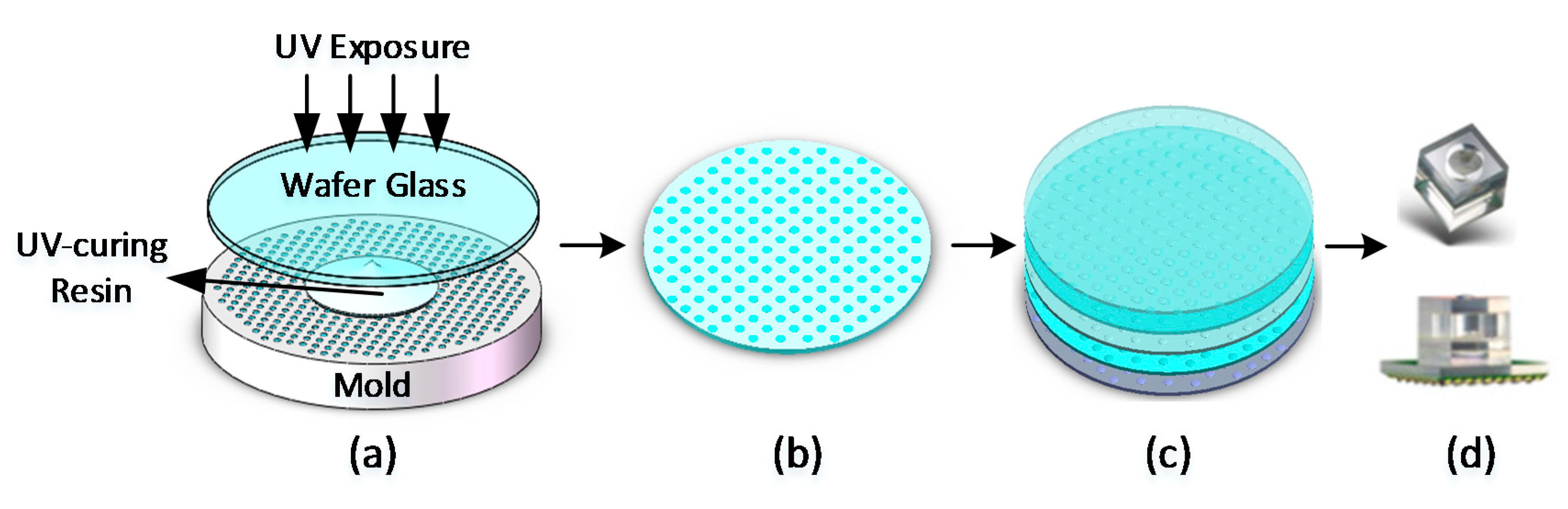
The wafer-level MLA is a thin, 4–8” diameter wafer, distributed with thousands of microlenses. As shown in Figure 1, the UV-curable resin-based imprint process transfers the microlens shape on the metal mold to a glass wafer substrate, which is free of high pressure, and then the wafer-level microlens array is released from the mold after curing. Several MLA wafers can be stack-assembled and cut into thousands of multisurface lens modules, resulting in very compact microcameras or camera arrays [26]. Currently, the wafer-level MLA process is mainly used to fabricate compact lens modules for low-resolution near-infrared (NIR) eye-ball tracking cameras or disposable endoscope modules. The general requirements of MLA surface characteristics are a PV error <0.5 μm with a sharp edge, a surface roughness (Sa) <20 nm, and a Fresnel reflectivity <1% to increase sensitivity and avoid ghost images. The wafer-level MLA mold is one of the core components in the whole process. Here, the fabrication of wafer-level MLA molds is followed by an AAO-based self-assembly process to provide periodically arranged nanostructuring.
The common ultraprecision machining methods used to generate precision MLA metal molds include fast tool servo (FTS), micromilling, and slow slide servo (SSS) processes [21,22,27]. In this study, micromilling and SSS diamond-machining processes were adopted to fabricate the MLA metal molds, using an ultraprecision machine (350FG, Moore Nanotechnology, Swanzey, NH, USA). For low-density arrays, the SSS-machining process was selected, as its implementation requires only 3 axes of freedom. For high-density MLA molds, the micromilling process was selected, as it allows more flexibility in large-slope microlens design.
The key factors that decide the quality of the MLA mold include the lenslet profile accuracy, mold surface roughness, and the lenslet positioning accuracy, which are closely related to the metal mold material, the diamond-machining performance, the machine-tool lifetime, and the machining process parameters. The mold material is the most crucial influencing factor. Metal materials that are used conventionally in diamond machining are usually high-ductility metals, such as aluminum and its alloys, copper alloys, and electroless nickel. Here, considering the further fabrication of nanostructures, various aluminum materials were selected as candidates for mold materials, namely 6061-T6 aluminum alloy, high-purity polycrystalline aluminum, and pure nanocrystalline aluminum.
Wafer-level MLA trial molds based on these aluminum materials were diamond-machined and evaluated according to the mold requirements. For the following machining tests, we designed the MLA aspherical shape with the cavity aperture at 1.0 mm and the sag at 85 μm. 6061-T6 aluminum alloy is the most widely diamond-machined material owing to its relatively high ductility and strength. A 6061-T6 4” MLA mold with a 20 × 20 array was machined via the SSS process. The nose radius of the single-point diamond tool was 0.3 mm, the spindle rotational speed was ~100 rpm, and the diamond tool traveled from the periphery to the center of the mold at a speed of 1 mm/min. The depth of the cut for a rough cut was 70 μm, the semifinished depth of the cut was 8 μm, and the finished depth of the cut was 2 μm. Next a high-purity polycrystalline aluminum pin mold was machined via the traditional diamond-turning method. Finally, we adopted the micromilling process for the 2” pure nanocrystalline aluminum MLA mold to create a dense lenslet array.
To generate a uniform layer of nanostructures on the MLA mold, we adopted the two-step AAO process, which is widely used for nanoporous template applications [28,29]. In the AAO experiments, we investigated characteristics, such as pore size, interpore distance, and nanolayer thickness, by varying the applied voltage, electrolyte concentration, and reaction time. In the first anodization step, the clean MLA mold was anodized in oxalic acid solution at 25 °C, the voltage was set at 40−50 V, and then a mixed solution of H3PO4 and H2CrO4 was used to remove the oxidized layer. Then, a pore-widening process was carried out using H3PO4 for 30 min. After optimizing the parameters of the anodization process, the nanostructured mold was finally fabricated with an average pore diameter of ~100 nm and a spatial period of ~120 nm. However, it needs to be clarified whether the AAO process is effective on curved array surfaces and whether the process will destroy the surface accuracy and roughness of mirror-quality precision molds.
2.2. Characterization
The proposed multiscale wafer-level MLA mold needed to satisfy the requirements for the lens mold profile, the surface roughness, and the nanostructure quality of the curved lens mold. The surface profiles of the MLA mold trial samples were obtained using a phase grating interferometer (PGI) Dimension stylus profiler (Taylor Hobson, Leicester, UK). The surface roughness was measured using a white light interference microscope (GTK-contour, Bruker, Billica, MA, USA), based on regional topography (Sa). Finally, the surface nanostructure morphology of the molds was characterized using a Zeiss SEM (Carl Zeiss Microscopy GmbH, Jena, Germany), after the AAO process.
3. Results and Discussion
3.1. 6061-T6 Aluminum Alloy MLA Mold
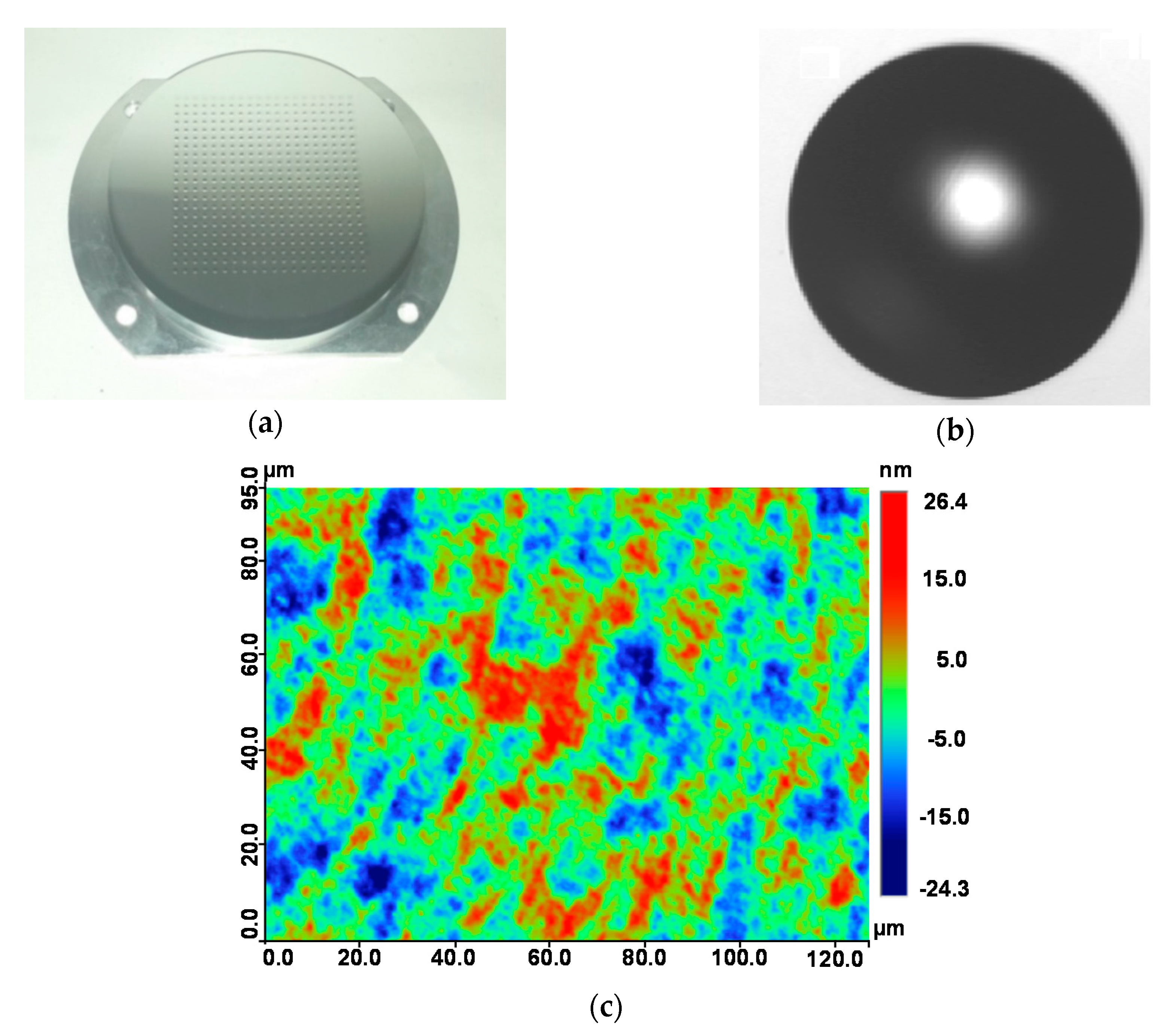
Figure 2a shows a photograph of the MLA mold fabricated with 6061-T6 aluminum alloy. Visual inspection did not indicate any surface artifacts, such as tool marks or haze, indicating that a true optical surface finish was achieved. Figure 2b demonstrates that the boundary of the lenslet has a sharp appearance with neither tool marks nor a tool tracking error. Figure 2c shows the surface 3D microtopology of the lenslet apex region. Curvature and tilt were removed from the measurement results to better represent the high spatial frequency of the surface texture. The surface roughness of the mold was 4.932 nm—this value meets the requirements for optical surface applications.
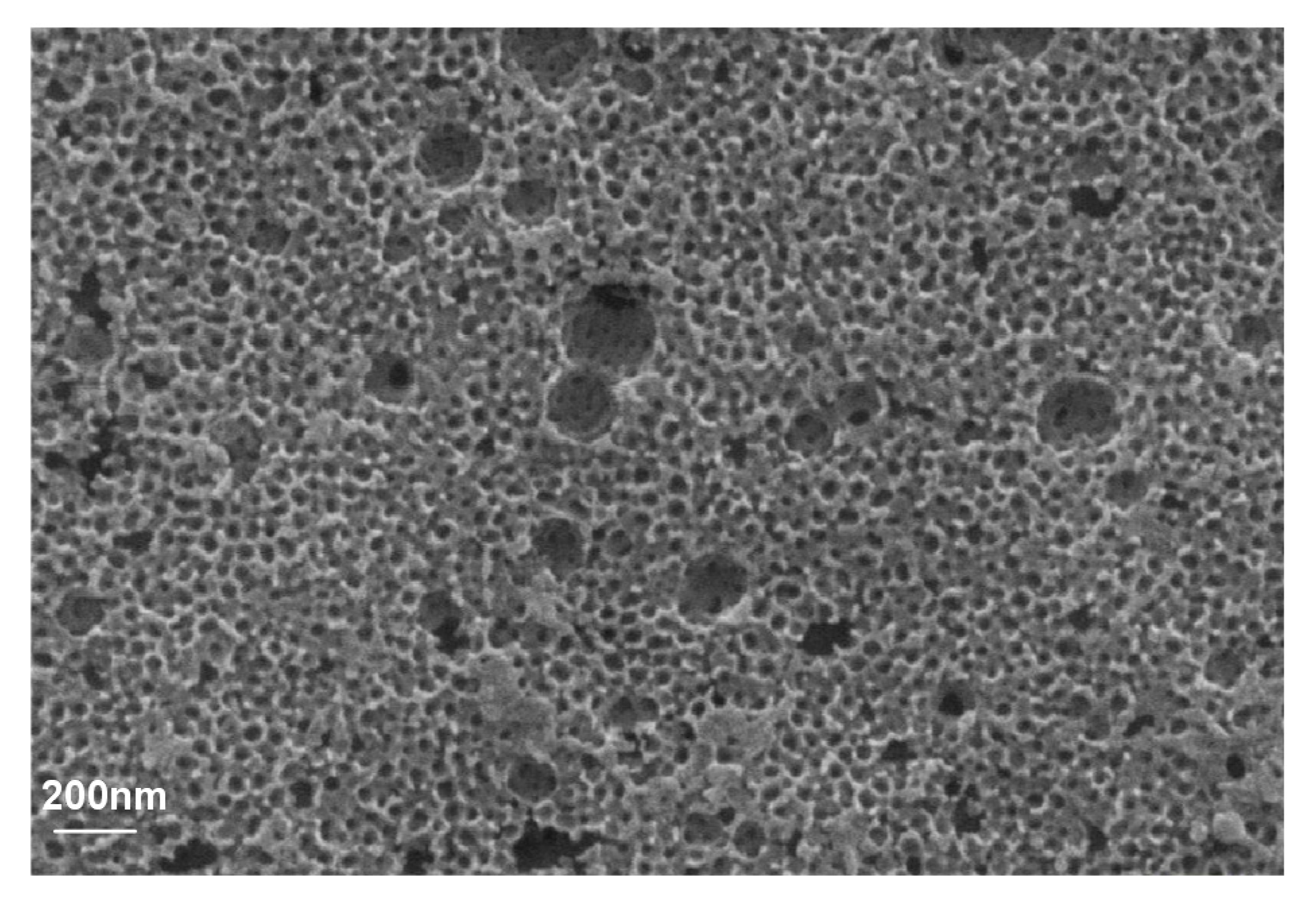
We then applied the AAO process to generate a uniform layer of nanostructures on the aluminum alloy MLA mold, as mentioned above. 6061-T6 aluminum alloy contains a variety of alloying elements, including magnesium and silicon. During the anodizing process, these alloying elements react to form nonuniform random nanopores and partial defects, as shown in Figure 3. At the same time, the nanopores are not uniform in either shape or depth. The nanostructured surface thus turns into a nonspecular surface. Therefore, the 6061-T6 MLA mold can meet the requirements of an optical mold, but it is not suitable for fabricating nanostructured MLAs.
3.2. High-Purity Polycrystalline Aluminum Pin Mold
To avoid the formation of nonuniform nanostructures due to alloy impurities, high-purity polycrystalline aluminum (with a purity of over 99.99%) was used as the mold material in the subsequent experiment. However, during the single-point diamond SSS-turning process, the cutting edge of the diamond tool was severely damaged, because the pure polycrystalline aluminum was too soft for single-point SSS turning. Hence, a wafer-level MLA mold meeting the optical requirements could not be obtained. Therefore, a pure polycrystalline aluminum optical mold was fabricated via the pin-mold mode, as shown in Figure 4a. Pin molds can be used to fabricate wafer MLAs via a slower step and flash process. Since each pin mold contains only a single lens cavity, the traditional high-speed single-point diamond-turning method can be used. Figure 4b shows the edge profile of the pin mold—it has a sharp appearance. The surface roughness of the lenslet region was 3.632 nm (Figure 4c), which meets the requirements for optical applications.
The high-purity polycrystalline aluminum pin mold was treated with the AAO process. Figure 5a shows a SEM image of the lenslet apex region. A hexagonal lattice with well-defined nanopores was formed as desired, exhibiting a fundamental pitch of 120 nm and a pore diameter of ~90 nm. The results of the surface roughness measurements are shown in Figure 5b, which demonstrate that the pin mold meets the requirements for optical applications (Sa = 9.161 nm). However, it also indicates that the polycrystalline aluminum surface is composed of multiple microsized grains. Figure 5c shows the 3D microtopology of the lens mold after one replication, which clearly indicates a surface profile deformation due to grain interfacial sliding under the demolding force. Consequently, the poor strength and shape stability of the pure crystalline pin mold restrict its application in wafer MLA manufacturing.
3.3. Pure Nanocrystalline Aluminum MLA Mold with Dense Array
After numerous trials to identify the right material, such as single crystal/polycrystalline pure aluminum and different aluminum alloys, an aluminum alloy (6061-T6) substrate electroplated with ~0.3 mm-thick pure aluminum consisting of nanosized grains (AlumiPlate, Coon Rapids, MN, US) was finally selected as the mold material, by considering the requirements of both the ultraprecision machining process and the subsequent AAO process. The strength of the 6061-T6 alloy substrate assures the shape stability of the mold, while the pure nanocrystalline-plated layer simultaneously supports the generation of a uniform nanopore layer without impurity defects. A 2” wafer mold was fabricated to validate the process. First, a flat optical surface was created on the aluminum substrate by a diamond-turning process, as shown in Figure 6a. Next, a concave MLA with a dense array was machined by micromilling using a high-speed air-bearing spindle. The measured results demonstrated that the boundary of the lenslets had a sharp appearance, as shown in Figure 6b. The surface roughness of the lenslet was 3.362 nm, as shown in Figure 6c. We then adopted the AAO process to obtain the pure nanocrystalline aluminum-dense MLA mold with nanostructures, as shown in Figure 6d.
The SEM images of the mold nanostructure, in Figure 7, show the uniformity of the nanoporous layer on the MLA mold cavity, both at the apex flat region and the lens boundary region. Cross-sectional SEM images of the thick metal mold were difficult to record, so Figure 7d shows a SEM image of a nanostructured sheet plate sample that was fabricated using the same process parameters as those of the metal mold. The nanostructures exhibited a V-shaped cross section with an average pore diameter of ~100 nm and a spatial period of ~120 nm, as shown in Figure 7d. Figure 8a shows the lens profile error of the lenslet mold with AR nanostructures—the PV error is ~0.098 μm, which indicates that the AAO process has little negative impact on the mold profile. The surface roughness of the nanostructured mold was measured to be 15.683 nm, as shown in Figure 8b, and the mold surface displays almost the same visual mirror quality as before the AAO treatment. The results of the surface profile and the surface roughness measurements showed that the MLA mold of pure nanocrystalline aluminum meets the optical requirements even after the nanostructuring treatment, and it paves the way for a further study to replicate a multiscale wafer-level MLA with an inherent AR capability.
4. Conclusions
In this study, three different aluminum materials were selected to fabricate multiscale wafer-level MLA molds with uniform nanostructures. After the trials with different materials, a 6061-T6 substrate, electroplated with pure aluminum consisting of nanosized grains (US proprietary), was identified to satisfy the requirements of both lens mold quality and uniform nanostructure. We demonstrated the fabrication of a high-quality, multiscale-structure wafer-level MLA mold using ultraprecision machining and self-assembling AAO processes, which produced hundreds of accurate aspherical microlens cavities and a uniform layer of AR nanostructures on the mold surface. The surface measurements indicated that the fabricated mold met the requirements for precision optical applications.
Compared with the former reports of AR nanostructured planar or flexible material molds, for the first time, this study generated AR nanostructures on a hard mold with densely arrayed lens surfaces and quantitatively evaluated its quality based on lens requirements. This study is expected to benefit the industrial production of novel and functional multiscale-structure wafer-level MLAs, as it provides a practical method for the manufacture of large wafer-level molds with high-quality and uniform nanostructures.
Author Contributions
Conceptualization and design of experiments, S.X., X.W. (Xinjun Wan), and X.W. (Xiaoxiao Wei); fabrication, S.X.; scanning electron microscopy (SEM) measurements, S.X.; data analysis, S.X., X.W. (Xinjun Wan), and X.W. (Xiaoxiao Wei); writing—original draft preparation, S.X.; writing—review and editing, X.W. (Xinjun Wan).
Funding
This work was funded by the National Natural Science Foundation of China under 61505107, the Capacity Building of Local Institutions of Shanghai Science and Technology Commission under 18060502500 and the National Key Scientific Instrument and Equipment Development Projects under 2012YQ170004.
Acknowledgments
The authors gratefully acknowledge the assistance of Yun Zhu from Shangmu Tech. who participated in the fabrication of the nanostructures.
Conflicts of Interest
The authors declare no conflict of interest.
References
- Cho, M.; Daneshpanah, M.; Moon, I.; Javidi, B. Three-Dimensional Optical Sensing and Visualization Using Integral Imaging. Proc. IEEE 2011, 99, 556–575. [Google Scholar]
- Tanida, J.; Kitamura, Y.; Yamada, K.; Miyatake, S.; Miyamoto, M.; Morimoto, T.; Masaki, Y.; Kondou, N.; Miyazaki, D.; Ichioka, Y. Compact image capturing system based on compound imaging and digital reconstruction. Proc. SPIE 2001, 4455, 34–41. [Google Scholar]
- Aldalali, B.; Li, C.; Zhang, L.; Jiang, H. Micro Cameras Capable of Multiple Viewpoint Imaging Utilizing Photoresist Microlens Arrays. J. Microelectromech. Syst. 2012, 21, 945–952. [Google Scholar] [CrossRef]
- Buettner, A.; Zeitner, U.D. Wave optical analysis of light-emitting diode beam shaping using microlens arrays. Opt. Eng. 2002, 41, 2393–2401. [Google Scholar] [CrossRef]
- Seifert, L.; Liesener, J.; Tiziani, H.J. The adaptive Shack–Hartmann sensor. Opt. Commun. 2003, 216, 313–319. [Google Scholar] [CrossRef]
- Wippermann, F.; Zeitner, U.D.; Dannberg, P.; Bräuer, A.; Sinzinger, S. Beam homogenizers based on chirped microlens arrays. Opt. Express 2007, 15, 6218–6231. [Google Scholar] [CrossRef] [PubMed]
- Buschbeck, E.; Ehmer, B.; Hoy, R. Chunk versus point sampling: Visual imaging in a small insect. Science 1999, 286, 1178–1180. [Google Scholar] [CrossRef]
- Andreas, B.; Jacques, D.; Robert, L.; Peter, D.; Andreas, B.U.; Andreas, T. Thin wafer-level camera lenses inspired by insect compound eyes. Opt. Express 2010, 18, 24379–24394. [Google Scholar]
- Raut, H.K.; Ganesh, V.A.; Nair, A.S.; Ramakrishna, S. Anti-Reflective Coatings: A Critical, In-Depth Review. Energy Environ. Sci. 2011, 4, 3779–3804. [Google Scholar] [CrossRef]
- Walheim, S.; Schäffer, E.; Mlynek, J.; Steiner, U. Nanophase-Separated Polymer Films as High-Performance Antireflection Coatings. Science 1999, 283, 520–522. [Google Scholar] [CrossRef]
- Mano, I.; Uchida, T.; Taniguchi, J. Fabrication of the antireflection structure on aspheric lens surface and lens holder. Microelectron. Eng. 2018, 191, 97–103. [Google Scholar] [CrossRef]
- Bae, B.J.; Hong, S.H.; Kwak, S.U.; Lee, H. Fabrication of Moth-Eye Pattern on a Lens Using Nano Imprint Lithography and PVA Template. J. Korean Inst. Surf. Eng. 2009, 42, 41–173. [Google Scholar] [CrossRef]
- Tan, G.; Lee, J.H.; Lan, Y.H.; Wei, M.K.; Peng, L.H.; Cheng, I.; Wu, S.T. Broadband antireflection film with moth-eye-like structure for flexible display applications. Optica 2017, 4, 678. [Google Scholar] [CrossRef]
- Hung, S.Y.; Chang, T.Y.; Shen, M.H.; Yang, H. Tilted microlens fabrication method using two photoresists with different melting temperatures. J. Micromech. Microeng. 2014, 24, 68–75. [Google Scholar] [CrossRef]
- Kim, S.; Kim, H.; Kang, S. Development of an ultraviolet imprinting process for integrating a microlens array onto an image sensor. Opt. Lett. 2006, 31, 2710–2712. [Google Scholar] [CrossRef] [PubMed]
- Chen, L.; Kirchberg, S.; Jiang, B.Y.; Xie, L.; Jia, Y.L.; Sun, L.L. Fabrication of long-focal-length plano-convex microlens array by combining the micro-milling and injection molding processes. Appl. Opt. 2014, 53, 7369–7380. [Google Scholar] [CrossRef] [PubMed]
- Zhang, J.; Shen, S.; Dong, X.X.; Chen, L.S. Low-cost fabrication of large area sub-wavelength anti-reflective structures on polymer film using a soft PUA mold. Opt. Express 2014, 22, 1842–1851. [Google Scholar] [CrossRef]
- Chidambaram, N.; Kirchner, R.; Altana, M.; Schift, H. High fidelity 3D thermal nanoimprint with UV curable polydimethyl siloxane stamps. J. Vac. Sci. Technol. B 2016, 34, 6K401. [Google Scholar] [CrossRef]
- Guo, R.; Xiao, S.; Zhai, X.; Li, J.; Xia, A.; Huang, W. Micro lens fabrication by means of femtosecond two photon photopolymerization. Opt. Express 2006, 14, 810–816. [Google Scholar] [CrossRef]
- Yan, J.H.; Ou, W.; Ou, Y.; Zhao, L.J. Design and fabrication of novel microlens–micromirrors array for infrared focal plane array. Microw. Opt. Technol. Lett. 2012, 54, 879–884. [Google Scholar]
- Yi, A.Y.; Li, L. Design and fabrication of a microlens array by use of a slow tool servo. Opt. Lett. 2005, 30, 1707–1709. [Google Scholar] [CrossRef] [PubMed]
- Yi, A.Y.; Huang, C.; Klocke, F.; Brecher, C.; Pongs, G.; Winterschladen, M.; Demmer, A.; Lange, S.; Bergs, T.; Merz, M.; et al. Development of a compression molding process for three-dimensional tailored free-form glass optics. Appl. Opt. 2006, 45, 6511–6518. [Google Scholar] [CrossRef] [PubMed]
- Mukaida, M.; Yan, J. Fabrication of Hexagonal Microlens Arrays on Single-Crystal Silicon Using the Tool-Servo Driven Segment Turning Method. Micromachines 2017, 8, 323. [Google Scholar] [CrossRef] [PubMed]
- Chang, X.; Xu, K.; Xie, D.; Luo, S.; Shu, X.; Ding, H.; Zheng, K.; Li, B. Microforging technique for fabrication of spherical lens array mold. Int. J. Adv. Manuf. Technol. 2018, 96, 3843–3850. [Google Scholar] [CrossRef]
- Gao, P.; Liang, Z.; Wang, X.; Zhou, T.; Xie, J.; Li, S.; Shen, W. Fabrication of a Micro-Lens Array Mold by Micro Ball End-Milling and Its Hot Embossing. Micromachines 2018, 9, 96. [Google Scholar] [CrossRef] [PubMed]
- Feldman, M.; America, T.N. Wafer-Level Camera Technologies Shrink Camera Phone Handsets. Photonic Spectra 2009, 41, 58–60. [Google Scholar]
- Zhan, Z.; Liang, N.; Bian, R.; Zhao, M. Design and Manufacturing of Ultra-Hard Micro-Milling Tool. Trans. Tianjin Univ. 2014, 20, 415–421. [Google Scholar] [CrossRef]
- Huangfu, Y.; Zhan, W.; Hong, X.; Fang, X.; Ding, G.; Ye, H. Heteroepitaxy of Ge on Si(001) with pits and windows transferred from free-standing porous alumina mask. Nanotechnology 2013, 24, 185302. [Google Scholar] [CrossRef] [PubMed]
- Ding, J.; Zhu, Y.; Yuan, N.; Ding, G. Reduction of nanoparticle deposition during fabrication of porous anodic alumina. Thin Solid Film 2012, 520, 4321–4325. [Google Scholar] [CrossRef]
Figure 1.
Wafer-level camera fabrication and assembly process, which creates extremely thin camera modules: (a) replication of microlens array using a mold, (b) wafer-level microlens array, (c) wafer-to-wafer bonding, and (d) dicing of wafer stack and bonding of the lens module to the sensor. UV: ultraviolet.

Figure 2.
Finished 6061-T6 aluminum alloy mold: (a) photograph of the processed sample of the dense microlens array (MLA) mold (20 × 20 array), (b) edge profile of the processed sample, and (c) surface roughness of the aluminum alloy MLA mold (Sa = 4.932 nm).
Figure 2.
Finished 6061-T6 aluminum alloy mold: (a) photograph of the processed sample of the dense microlens array (MLA) mold (20 × 20 array), (b) edge profile of the processed sample, and (c) surface roughness of the aluminum alloy MLA mold (Sa = 4.932 nm).

Figure 3.
Scanning electron microscopy (SEM) image of the nanostructured 6061-T6 MLA mold.

Figure 4.
Finished high-purity polycrystalline aluminum pin mold: (a) photograph of the processed sample of the pin mold, (b) edge profile of the processed sample, and (c) surface roughness of the polycrystalline aluminum pin mold (Sa = 3.632 nm).
Figure 4.
Finished high-purity polycrystalline aluminum pin mold: (a) photograph of the processed sample of the pin mold, (b) edge profile of the processed sample, and (c) surface roughness of the polycrystalline aluminum pin mold (Sa = 3.632 nm).


Figure 5.
(a) SEM image of the lenslet mold apex region. (b) Surface roughness of the nanostructured pin mold (Sa = 9.161 nm). (c) The lens mold 3D microtopology after one replication (Sa = 48.939 nm).
Figure 5.
(a) SEM image of the lenslet mold apex region. (b) Surface roughness of the nanostructured pin mold (Sa = 9.161 nm). (c) The lens mold 3D microtopology after one replication (Sa = 48.939 nm).

Figure 6.
Different stages in the fabrication of the hybrid-structure microlens array (MLA) metal wafer mold: photographs of (a) the flat mirror surface obtained by diamond-turning and (b) the micromilled MLA mold cavities on the substrate and edge profile of the processed sample, (c) the MLA mold 3D surface finish of the lenslet apex region without nanostructures (Sa = 3.362 nm), and (d) the final MLA mold with antireflection nanostructures, which was fabricated using the anodic aluminum oxidation (AAO) process.

Figure 7.
(a) SEM images of the nanostructured MLA mold. (b) High-magnification SEM image of the lenslet apex region. (c) High-magnification SEM image of the lenslet boundary region, with the boundary being indicated by the dashed line. (d) Cross-sectional SEM image of the nanopores.
Figure 7.
(a) SEM images of the nanostructured MLA mold. (b) High-magnification SEM image of the lenslet apex region. (c) High-magnification SEM image of the lenslet boundary region, with the boundary being indicated by the dashed line. (d) Cross-sectional SEM image of the nanopores.

Figure 8.
(a) Stylus profile measurement results of the lenslet mold with nanostructures (peak-to-valley (PV) error = 0.0985 μm). (b) Surface roughness of the MLA mold with nanostructures (Sa = 15.683 nm).
Figure 8.
(a) Stylus profile measurement results of the lenslet mold with nanostructures (peak-to-valley (PV) error = 0.0985 μm). (b) Surface roughness of the MLA mold with nanostructures (Sa = 15.683 nm).

© 2019 by the authors. Licensee MDPI, Basel, Switzerland. This article is an open access article distributed under the terms and conditions of the Creative Commons Attribution (CC BY) license (http://creativecommons.org/licenses/by/4.0/).
Share and Cite
MDPI and ACS Style
Xie, S.; Wan, X.; Wei, X. Fabrication of Multiscale-Structure Wafer-Level Microlens Array Mold. Appl. Sci. 2019, 9, 487. https://doi.org/10.3390/app9030487
AMA Style
Xie S, Wan X, Wei X. Fabrication of Multiscale-Structure Wafer-Level Microlens Array Mold. Applied Sciences. 2019; 9(3):487. https://doi.org/10.3390/app9030487
Chicago/Turabian StyleXie, Shuping, Xinjun Wan, and Xiaoxiao Wei. 2019. "Fabrication of Multiscale-Structure Wafer-Level Microlens Array Mold" Applied Sciences 9, no. 3: 487. https://doi.org/10.3390/app9030487
Note that from the first issue of 2016, this journal uses article numbers instead of page numbers. See further details here.