Effect of 0.05 wt.% Pr Addition on Microstructure and Shear Strength of Sn-0.3Ag-0.7Cu/Cu Solder Joint during the Thermal Aging Process


1
College of Materials Science and Technology, Nanjing University of Aeronautics and Astronautics, Nanjing 210016, China
2
Department of Mechanical, Aerospace and Biomedical Engineering, University of Tennessee Knoxville, Knoxville, TN 37996, USA
*
Author to whom correspondence should be addressed.
Appl. Sci. 2019, 9(17), 3590; https://doi.org/10.3390/app9173590
Submission received: 1 August 2019
/
Revised: 21 August 2019
/
Accepted: 22 August 2019
/
Published: 2 September 2019
(This article belongs to the Special Issue Metal Matrix Composite)
Abstract
:The evolution of interfacial morphology and shear strengths of the joints soldered with Sn-0.3Ag-0.7Cu (SAC0307) and SAC0307-0.05Pr aged at 150 °C for different times (h; up to 840 h) were investigated. The experiments showed the electronic joint soldered with SAC0307-0.05Pr has a much higher shear strength than that soldered with SAC0307 after each period of the aging process. This contributes to the doping of Pr atoms, “vitamins in alloys”, which tend to be adsorbed on the grain surface of interfacial Cu6Sn5 IMCs, inhibiting the growth of IMCs. Theoretical analysis indicates that doping 0.05 wt.% Pr can evidently lower the growth constant of Cu6Sn5 (DCu6), while the growth constant of Cu3Sn (DCu3) decreased slightly. In addition, the electronic joint soldered with SAC0307-0.05Pr still has better ductility than that soldered with SAC0307, even after a 840-h aging process.

1. Introduction
In microelectronic packaging, solder joints play an electrical, mechanical, and thermal role between electronic devices and conductive substrates [1,2]. With miniaturized trends of integrated circuits in electronic devices, the reliability of solder joints becomes particularly important, especially in severe environments, such as high-temperature aging, thermal cycling, drop reliability, and so on [3,4,5].
In consideration of close relationship between microstructures and properties, interfacial microstructure at the solder–substrate interface should be studied to enhance the mechanical reliability of the joint. Numerous studies [6,7,8] have already demonstrated that one solder with more refined microstructures and thinner interfacial intermetallic compound (IMC) layers usually has a better joint reliability. To achieve this, several research groups are focused on developing composite materials doped with different types of micro- and nano-scale metallic e.g., Ag [9], Ni [10], In [11], Al [12], Co [13]; ceramic e.g., TiO2, ZrO2, Al2O3, and TiO2 etc. [9,14,15,16] and rare earth (RE) elements [17,18,19]. This is because most of these reinforcements are surface-active and prone to have adsorptions on the surfaces of the grain. Therefore, a pinning effect was exerted by them on grain growth. Sadiq et al. [20] studied the effect of RE La on the microstructures and mechanical properties of SAC alloy at a temperature of 150 °C. Corresponding results showed that the average grain size of IMCs distributed in La-doped solder was refined by up to 40% and the coarsening rate of the IMCs is slowed by 70% when compared with those in the non-doped solder. Corresponding yield stress and tensile strength are enhanced by 20% by minute lanthanum doping. In addition, the aging of nanoparticle-doped solder was also investigated, such as SAC387 solder doped with Co nanoparticle aging at 150 °C for up to 1200 h. It was found that Co nanoparticles effectively suppressed the growth of interfacial Cu3Sn IMCs but contribute to the growth of Cu6Sn5. Co nanoparticles will also experience surface dissolution during reflow processes [21]. Although nanoparticles are the research hotspot presently, doping technology and agglomeration are still key issues that remain to be resolved, especially for the economically and easily available ceramic nanoparticles [22,23,24]. Hence, in this study, RE Pr was taken to modify microstructure and properties of solders based on previous research on solders modified by RE alloys [17,18]. For solder selection, lead-free solder has been adopted in this study according to the directives of Waste Electrical and Electronic Equipment (WEEE) and Restriction of Hazardous Substances (RoHS) [25]. Among the alternative lead-free Sn-based solder alloys such as Sn-9Zn (198 °C), Sn-58Bi (138 °C), Sn-3.5Ag (221 °C), Sn-0.7Cu (221 °C), and Sn-3.0Ag-0.5Cu (217 °C) [26,27,28,29], Sn-Ag-Cu has received wide acceptance due to its superior comprehensive properties. However, for fear of plate-like Ag3Sn IMCs in Sn-Ag-Cu high-Ag solder ruining its drop reliability [7], the content of Ag was decreased to 0.3 wt.% in this study.
Lots of previous research has only focused on studying RE alloys on the microstructure of solder matrixes and solid–liquid reactions during soldering processes, whereas the reaction mechanism during solid–solid processes should also be given attention. This could help researchers to better understand the detailed failure mechanism of electronic device in service. Hence, this work is devoted to investigating the evolution of interfacial microstructures and the shear strength of SAC0307/Cu and SAC0307-0.05Pr/Cu solder under isothermal aging treatment (150 °C; up to 840 h). In addition, the effect of 0.05 wt.% Pr on the detailed growth kinetics of interfacial morphology at SAC0307 solder/Cu substrate interface during solid–solid reactions were also analyzed.
2. Materials and Methods
SAC0307 alloy was prepared by fusing Sn, Ag, and Cu (Purity: 99.95 wt.%) at 900 °C ± 10 °C. For fear of RE oxidation, RE Pr was doped in the Sn-Ag-Cu alloy mixture in the form of Sn-10Pr and the melting temperature was adjusted to 550 ± 1 °C. Finally, SAC0307-0.05Pr was obtained by diluting the above alloy mixture and then was shaped into bars.
Specimens for high-temperature aging were sliced from a cast sample. Interfacial specimens were made by soldering the examined solders (SAC0307; SAC0307-0.05Pr) onto Cu substrate. The aging temperature and time was selected as 150 °C and 840 h, respectively. For microstructure observation, specimens were polished with 0.3 μm Al2O3 suspension and then etched with the corrosion liquid (4% HNO3-alcohol). Microstructure observation was conducted by optical microscope, Scanning electron microscope (SEM), and Energy dispersive spectrum (EDS) analysis. In addition, Image Pro-Plus software was used to calculate IMC layer’s thickness.
The shear strengths of corresponding joints after each aging period were measured by a joint strength tester (Mode: STR-1000). The joint specimens made through soldering ceramic resistors (0805) on Cu substrates were put into a high-temperature environment. After shear loading, the fractographs of shear joints were studied by SEM and EDS.
3. Results and Discussion
3.1. Microstructure Evolution after Isothermal Aging
Figure 1 provided the microstructure of SAC0307, SAC0307-0.05Pr, and their aged samples (up to 840 h). As can be seen, solder doped with 0.05 wt.% Pr has a much more refined microstructure (Figure 1b) when compared with the original SAC0307 solder (Figure 1a). Obviously, IMCs in the eutectic area distributing on the Sn matrix in SAC0307-0.05Pr solder were much more refined than those in SAC0307 solder. In addition, the amount of eutectic areas was also increased after doping 0.05 wt.% Pr. After an 840-h aging treatment, IMCs in the eutectic area whether in the aged SAC0307 solder or in the aged SAC0307-0.05Pr solder grew larger (Figure 1c,d). However, the average size of the related IMCs in the aged SAC0307 were still larger in the aged SAC0307-0.05Pr and the amount of eutectic areas was also smaller than those in SAC0307-0.05Pr. It should be noted that PrSn3 phase with flower shape [30] emerged in the aged SAC0307-0.05Pr solder. Figure 1e shows the SEM image of the microstructure of aged SAC0307-0.05Pr. Also, PrSn3 phase with the similar shape as that in Figure 1d can be clearly seen, which was demonstrated by the EDS analysis of Point 1, shown in Table 1. It was largely because RE Pr is a Sn-affinity element. With aging treatment, Sn and Pr atom diffusion were accelerated and finally they were reacted as PrSn3. In addition, IMCs in the eutectic area was also analyzed by EDS technique and the results showed the darker ones are mainly Cu6Sn5 and the bright ones are Ag3Sn IMCs. Figure 2 gives the detailed illustration of changes in IMCs in both SAC0307 and SAC0307-0.05Pr solders during aging process. Usually, IMCs in SAC0307 grow larger with a certain rate depending on Sn, Ag, and Cu atom diffusion rates, as can be seen from Figure 2(aI–III). For SAC0307 with 0.05 wt.% Pr doped, the growth of IMCs in the eutectic area with aging process was hindered since the surface-active Pr atoms tend to adsorb on the grain surface of IMCs. Hence, the diffusion of Sn, Ag, and Cu atoms were inhibited, as shown in Figure 2(bI–III).
Figure 3 and Figure 4 show changes of interfacial microstructures of SAC0307/Cu and SAC0307-0.05Pr/Cu joint subjected to different length of time of aging process. For the interfacial microstructure of SAC0307/Cu solder, a continuous hill-like Cu6Sn5 interfacial IMC layer [31] with sharp protrusions emerged after initial 72-h aging (Figure 3a). Moreover, a darker interfacial IMC layer, as identified to be Cu3Sn [32] also grew near the Cu substrate. As aging time prolongs to 840 h, the radius of Cu6Sn5 increased with the number decreasing (Figure 3b–d). In addition, the thickness of Cu3Sn also increased, and a detailed calculation is conducted in next section. In contrast to interfacial IMCs’ growth at SAC0307/Cu interface with aging, Cu6Sn5 IMCs at SAC0307-0.05Pr/Cu interface were developed without any sharp Cu6Sn5 protrusions and the interfacial IMC layer was much more flat than the original aged one, even with aging treatment (Figure 4a–d). In addition, the growth of Cu3Sn was also much slower than that at the SAC0307-0.05Pr/Cu interface. Figure 5 provides the changes in interfacial IMCs at both SAC0307 solder/Cu interface and SAC0307-0.05Pr solder/Cu interface during the aging process. Without Pr addition, the interfacial IMCs grows at a certain rate depending on the diffusions of Sn atoms from solder and Cu atoms from Cu substrate to the solder/Cu6Sn5 or Cu6Sn5/Cu3Sn and Cu3Sn/Cu interface. Hence, the shape of interfacial Cu6Sn5 IMCs varied with aging due to different diffusion rate of atoms (Figure 5(aI–III)). However, with a minute amount of Pr addition, the interfacial Cu6Sn5 IMCs became flatter due to the Pr atoms adsorbing on the surface of Cu6Sn5 IMCs, hindering their growth, as shown in Figure 5(bI). With aging going on, the diffusion of Sn and Cu atoms were largely affected by RE Pr atoms and the shape of interfacial IMC layer remains flat, as illustrated in Figure 5(bII,III).
3.2. Thickness Changes of Interfacial IMC Layer during Isothermal Aging
For interfacial IMC layers at both interfaces of SAC0307/Cu and SAC0307-0.05Pr/Cu, the thickness of Cu6Sn5 and Cu3Sn IMC layers raised with aging time, as summarized in Table 2. With 840 h aging, the total interfacial IMC layer thickness at SAC0307/Cu interface grew to 10.2 μm, whereas that at the SAC0307-0.05Pr/Cu increased only to 6.5 μm. In addition, Cu3Sn IMC layers’ thicknesses at these two types of interfaces reached 4.9 μm and 3.9 μm, respectively. Obviously, a minute amount of Pr effectively hindered the growth of interfacial IMCs. Commonly, the growth and development of interfacial IMC layer is diffusion-controlled. The relationship between interfacial IMC layer thickness and aging time meets the following classic diffusion formula [16]:
where xt is interfacial IMC layer’s thickness change after one period of aging time t, x0 is its initial thickness, D is the growth coefficient, as calculated from the slope of the fitted curve of interfacial IMC layer thickness with aging time, as shown in Figure 6. The following lists the final results.
It can be calculated that the growth constant of total interfacial IMC layer (DT), Cu6Sn5 (DCu6), Cu3Sn (DCu3) for the SAC0307/Cu joint was 3.11 × 10⁻¹⁰ cm2/s, 0.12 × 10⁻¹⁰ cm2/s and 2.02 × 10⁻¹⁰ cm2/s, respectively, while that for SAC0307-0.05Pr/Cu joint was 1.65 × 10⁻¹⁰ cm2/s, 0.0021 × 10⁻¹⁰ cm2/s (approximate to 0), and 1.53 × 10⁻¹⁰ cm2/s, respectively. Obviously, doping 0.05 wt.% Pr can evidently lower the growth constant of Cu6Sn5 (DCu6), while the growth constant of Cu3Sn (DCu3) was decreased slightly. The decreased growth constant of Cu6Sn5 (DCu6) was mainly due to Pr atoms pinning on the growth of Cu6Sn5. The suppressed mechanism for interfacial Cu3Sn was mainly associated with a decreased gradient of Sn atom concentration at Cu6Sn5/Cu3Sn interface. In addition, it can be observed that the decreased level for the growth constant of interfacial Cu6Sn5 (DCu6) is much larger than that of DCu3. This can be explained as follows. Generally, there are two ways to form interfacial Cu6Sn5. One is forming directly through Sn and Cu atom diffusion.
6Cu + 5Sn→Cu6Sn5
The other is through sacrificing interfacial Cu3Sn,
2Cu3Sn + 3Sn→Cu6Sn5
For producing interfacial Cu3Sn IMCs, two approaches also can be reached. One is also forming directly:
3Cu + Sn→Cu3Sn
The other is developing through consuming interfacial Cu6Sn5 IMCs:
Cu6Sn5 + 9Cu→5Cu3Sn
It can be seen that for directly forming interfacial Cu6Sn5 and Cu3Sn IMCs (Equations (4) and (6)), per unit of Cu6Sn5 requires more Sn atoms than per unit of Cu3Sn. For indirectly forming them (Equations (5) and (7)), Cu3Sn just needs abundant supply of Cu atoms, whereas that of Cu6Sn5 still needs the supply of Sn atoms. Therefore, it can be concluded that what controls Cu6Sn5 IMCs’ growth is the Sn atom diffusion and the solder/Cu6Sn5 interface state, while Cu atom diffusion determines the interface state of Cu3Sn/Cu6Sn5 and determines the development of Cu3Sn. Obviously, most Sn source comes from Sn-based solder, while most Cu source is from Cu substrate. Although most Pr atoms were adsorbed on the Cu substrate, hindering Cu diffusion in the initial reaction period, its inhibition effect was mainly on Sn atom diffusion with the growth of Cu6Sn5. Therefore, the interfacial Cu6Sn5 IMC growth was affected more than Cu3Sn IMCs.
3.3. Shear Strength and Fracture Morphology after Aging Process
Figure 7a provides the corresponding illustration of shearing process and Figure 7b is the detailed plot between shear strength and aging time. Clearly, it can be observed that the shear strength of SAC0307-0.05Pr/Cu decreases with aging time at a certain rate, while the shear strength of SAC0307/Cu decreases also with a certain rate first but at a rapid decrease with aging time. After 840 h aging, the shear strengths of SAC0307/Cu and SAC0307-0.05Pr/Cu were declined to 9.5 MPa and 7.5 MPa, respectively. In addition, the shear strength of SAC0307-0.05Pr/Cu solder joint was larger than that of SAC0307/Cu solder joint after each aging process. This was mainly associated with their interfacial IMC layer’ growth, as explained above.
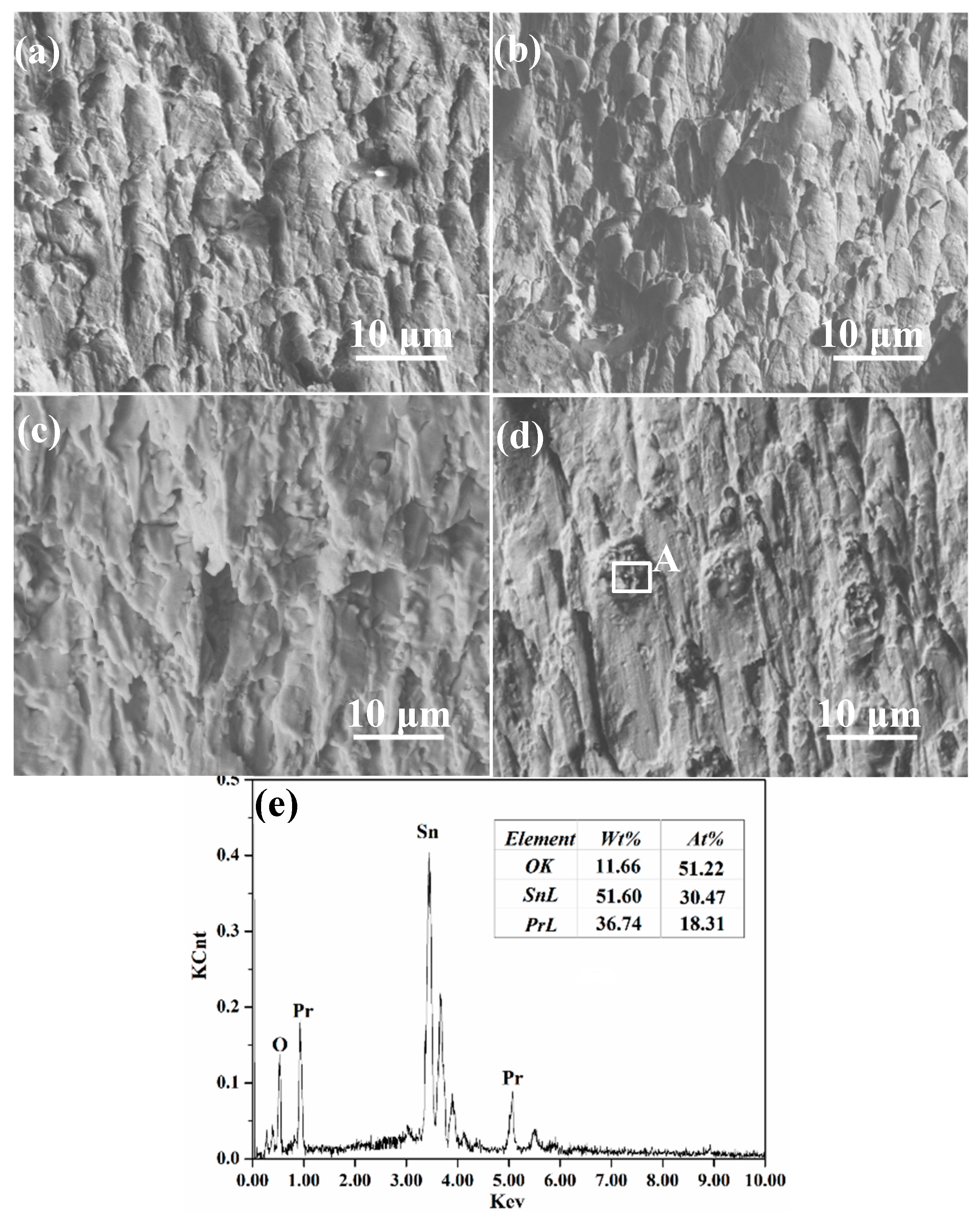
Figure 8 provides SEM images of corresponding fracture morphology at SAC0307/Cu, SAC0307-0.05Pr/Cu interfaces and the aged samples. Clearly, elongated dimples parallel to shear direction can be observed on the surface of fractured SAC0307/Cu shear joint, indicative of a distinct ductile fracture. For a fractograph of SAC0307-0.05Pr/Cu shear joint, dimples with smaller size emerge, indicating better ductility. After 840 h aging treatment, the dimples of these two types of joints became larger and more superficial, indicating the decrease in ductility with aging treatment. However, the average size of dimples on surface of fractured SAC0307-0.05Pr/Cu shear joint was still a bit larger than those on the fracture surface of SAC0307/Cu shear joint. It means the ductility of SAC0307-0.05Pr was still better than SAC0307/Cu solder even with 840 h aging. However, it should be noted that Pr oxides emerges on the fracture surface of SAC0307-0.05Pr/Cu shear joint after 840 h aging, possibly due to the appearance of PrSn3 in the aged SAC0307-0.05Pr solder microstructure (Figure 1d).
4. Conclusions
The effect of 0.05 wt.% Pr on high-temperature microstructure and shear strength of Sn-0.3Ag-0.7Cu/Cu low-Ag solder joint was studied and the following conclusions were obtained:
- SAC0307-0.05Pr solder has a more refined microstructure with smaller size of Cu6Sn5 IMCs distributed on Sn matrix after 840 h aging when compared to Sn-0.3Ag-0.7Cu solder. This is because of the inhibiting effect on IMCs’ growth by Pr atoms adsorbing on their grain surfaces.
- During aging process, two types of interfacial IMC layers (Cu6Sn5 + Cu3Sn) were gradually developed at solder/Cu interfaces and the thicknesses of them also increased with aging time. Theoretical analysis indicated that doping 0.05 wt.% Pr evidently lowered the growth constant of Cu6Sn5(DCu6), while the growth constant of Cu3Sn (DCu3) decreased slightly.
- SAC0307-0.05Pr/Cu solder joint has a higher shear strength than SAC0307/Cu solder joint even after 840 h aging. In this case, SAC0307-0.05Pr/Cu solder joint still has a better ductility than SAC0307/Cu.
Author Contributions
Investigation, J.W. (Jie Wu); Writing Original Draft Preparation, J.W. (Jie Wu); Writing, Review & Editing, S.X.; J.W. (Jingwen Wang); Supervision, S.X.; G.H.; Project Administration, J.W. (Jingwen Wang); Funding Acquisition, S.X.
Funding
This research was funded by [Songbai Xue] grant number [No. 51675269], by [Songbai Xue] grant number [No. 61605045] and by [Jie Wu] grant number [PAPD].
Acknowledgments
This project is supported by National Natural Science Foundation of China (Grant No. 51675269), National Natural Science Foundation of China (No. 61605045) and the Priority Academic Program Development of Jiangsu Higher Education Institutions (PAPD).
Conflicts of Interest
We declare no conflict of interest.
References
- Zhang, L.; Han, J.-G.; Guo, Y.; He, C.-W. Anand model and FEM analysis of SnAgCuZn lead-free solder joints in wafer level chip scale packaging devices. Microelectron. Reliab. 2014, 54, 281–286. [Google Scholar] [CrossRef]
- Tu, P.; Chan, Y.; Hung, K.; Lai, J.; Lai, J.K.L. Growth kinetics of intermetallic compounds in chip scale package solder joint. Scr. Mater. 2001, 44, 317–323. [Google Scholar] [CrossRef] [Green Version]
- Cheng, B.; Wang, L.; Zhang, Q.; Gao, X.; Xia, X.; Kempe, W. Flip chip solder joint reliability under harsh environment. Solder. Surf. Mt. Technol. 2003, 15, 15–20. [Google Scholar]
- Wu, J.; Xue, S.; Wang, J.-W.; Wang, J.-X.; Deng, Y. Enhancement on the high-temperature joint reliability and corrosion resistance of Sn-0.3Ag-0.7Cu low-Ag solder contributed by Al2O3 Nanoparticles (0.12 wt%). J. Mater. Sci. Mater. Electron. 2018, 29, 19663–19677. [Google Scholar]
- Chen, W.-H.; Yu, C.-F.; Cheng, H.-C.; Tsai, Y.-M.; Lu, S.-T. IMC growth reaction and its effects on solder joint thermal cycling reliability of 3D chip stacking packaging. Microelectron. Reliab. 2013, 53, 30–40. [Google Scholar] [CrossRef]
- Wu, J.; Xue, S.-B.; Wang, J.-W.; Liu, S.; Han, Y.-L.; Wang, L.-J. Recent progress of Sn–Ag–Cu lead-free solders bearing alloy elements and nanoparticles in electronic packaging. J. Mater. Sci. Mater. Electron. 2016, 27, 12729–12763. [Google Scholar] [CrossRef]
- Huang, M.-L.; Zhao, N.; Liu, S.; He, Y.-Q. Drop failure modes of Sn–3.0Ag–0.5Cu solder joints in wafer level chip scale package. Trans. Nonferrous Met. Soc. China 2016, 26, 1663–1669. [Google Scholar] [CrossRef]
- Mi, J.; Li, Y.-F.; Yang, Y.-J.; Peng, W.; Huang, H.-Z. Thermal Cycling Life Prediction of Sn-3.0Ag-0.5Cu Solder Joint Using Type-I Censored Data. Sci. World J. 2014, 2014. [Google Scholar] [CrossRef]
- Zhang, L.; Tu, K. Structure and properties of lead-free solders bearing micro and nano particles. Mater. Sci. Eng. R Rep. 2014, 82, 1–32. [Google Scholar] [CrossRef]
- Gain, A.K.; Zhang, L. Interfacial microstructure, wettability and material properties of nickel (Ni) nanoparticle doped tin-bismuth-silver (Sn-Bi-Ag) solder on copper (Cu) substrate. J. Mater. Sci. Mater. Electron. 2016, 27, 3982–3994. [Google Scholar] [CrossRef]
- Gnecco, F.; Ricci, E.; Amore, S.; Giuranno, D.; Borzone, G.; Zanicchi, G.; Novakovic, R. Wetting behaviour and reactivity of lead free Au-In-Sn and Bi-In-Sn alloys on copper substrates. Int. J. Adhes. Adhes. 2007, 27, 409–416. [Google Scholar] [CrossRef]
- Gain, A.K.; Zhang, L. Harsh service environment effects on the microstructure and mechanical properties of Sn–Ag–Cu-1 wt% nano-Al solder alloy. J. Mater. Sci. Mater. Electron. 2016, 27, 11273–11283. [Google Scholar] [CrossRef]
- Wang, Y.; Lin, Y.; Tu, C.; Kao, C. Effects of minor Fe, Co, and Ni additions on the reaction between SnAgCu solder and Cu. J. Alloys Compd. 2009, 478, 121–127. [Google Scholar] [CrossRef]
- Gain, A.K.; Zhang, L. Microstructure, mechanical and electrical performances of zirconia nanoparticles-doped tin-silver-copper solder alloys. J. Mater. Sci. Mater. Electron. 2016, 27, 7524–7533. [Google Scholar] [CrossRef]
- Gain, A.K.; Zhang, L.; Chan, Y.C. Microstructure, elastic modulus and shear strength of alumina (Al2O3) nanoparticles-doped tin-silver-copper (Sn-Ag-Cu) solders on copper (Cu) and gold/nickel (Au/Ni)-plated Cu substrates. J. Mater. Sci. Mater. Electron. 2015, 26, 7039–7048. [Google Scholar] [CrossRef]
- Tsao, L.C.; Chang, S.Y. Effects of Nano-TiO2 additions on thermal analysis, microstructure and tensile properties of Sn3.5Ag0.25Cu solder. J. Mater. Sci. Mater Electron. 2015, 26, 7039–7048. [Google Scholar] [CrossRef]
- Li, B.; Shi, Y.; Lei, Y.; Guo, F.; Xia, Z.; Zong, B. Effect of rare earth element addition on the microstructure of Sn-Ag-Cu solder joint. J. Electron. Mater. 2015, 34, 217–224. [Google Scholar] [CrossRef]
- Xiao, W.; Shi, Y.; Xu, G.; Ren, R.; Guo, F.; Xia, Z.; Lei, Y. Effect of rare earth on mechanical creep–fatigue property of SnAgCu solder joint. J. Alloys Compd. 2009, 472, 198–202. [Google Scholar] [CrossRef]
- Wu, J.; Xue, S.; Wang, J.; Wang, J.; Liu, S. Effect of Pr addition on properties and Sn whisker growth of Sn–0.3Ag–0.7Cu low-Ag solder for electronic packaging. J. Mater. Sci. Mater. Electron. 2017, 37, 1640–10244. [Google Scholar] [CrossRef]
- Sadiq, M.; Pesci, R.; Cherkaoui, M. Impact of Thermal Aging on the Microstructure Evolution and Mechanical Properties of Lanthanum-Doped Tin-Silver-Copper Lead-Free Solders. J. Electron. Mater. 2013, 42, 492–501. [Google Scholar] [CrossRef] [Green Version]
- Haseeb, A.; Leng, T.S. Effects of Co nanoparticle addition to Sn–3.8Ag–0.7Cu solder on interfacial structure after reflow and ageing. Intermetallics 2011, 19, 707–712. [Google Scholar] [CrossRef]
- Gu, Y.; Zhao, X.; Li, Y.; Liu, Y.; Wang, Y.; Li, Z. Effect of nano-Fe2O3 additions on wettability and interfacial intermetallic growth of low-Ag content Sn–Ag–Cu solders on Cu substrates. J. Alloys Compd. 2015, 627, 39–47. [Google Scholar] [CrossRef]
- Wu, J.; Xue, S.; Wang, J.; Wu, M.; Wang, J. Effects of α-Al2O3 nanoparticles-doped on microstructure and properties of Sn–0.3Ag–0.7Cu low-Ag solder. J. Mater. Sci. Mater. Electron. 2018, 29, 7372–7387. [Google Scholar] [CrossRef]
- Wu, J.; Xue, S.; Wang, J.; Wu, M. Coupling effects of rare-earth Pr and Al2O3 nanoparticles on the microstructure and properties of Sn-0.3Ag-0.7Cu low-Ag solder. J. Alloys Compd. 2019, 784, 471–487. [Google Scholar] [CrossRef]
- Yu, J.; Welford, R.; Hills, P. Industry responses to EU WEEE and ROHS directives: Perspectives from China. Corp. Soc. Responsib. Environ. Manag. 2012, 13, 286–299. [Google Scholar] [CrossRef]
- Kotadia, H.R.; Howes, P.D.; Mannan, S.H. A review: On the development of low melting temperature Pb-free solders. Microelectron. Reliab. 2014, 54, 1253–1273. [Google Scholar] [CrossRef]
- Gain, A.K.; Zhang, L. High-temperature and humidity change the microstructure and degrade the material properties of tin-silver interconnect material. Microelectron. Reliab. 2018, 83, 101–110. [Google Scholar] [CrossRef]
- Cheng, S.; Huang, C.-M.; Pecht, M. A review of lead-free solders for electronics applications. Microelectron. Reliab. 2017, 75, 77–95. [Google Scholar] [CrossRef]
- Gain, A.K.; Zhang, L. Growth nature of in-situ Cu6Sn5-phase and their influence on creep anddamping characteristics of Sn-Cu material under high-temperature and humidity. Microelectron. Reliab. 2018, 87, 278–285. [Google Scholar] [CrossRef]
- Chuang, T.; Lin, H. Size Effect of Rare-Earth Intermetallics in Sn-9Zn-0.5Ce and Sn-3Ag-0.5Cu-0.5Ce Solders on the Growth of Tin Whiskers. Met. Mater. Trans. A 2008, 39, 2862–2866. [Google Scholar] [CrossRef]
- Huang, J.Q.; Zhou, M.B.; Liang, S.B.; Zhang, X.P. Size effects on the interfacial reaction and microstructural evolution of Sn-ball/Sn3.0Ag0.5Cu-paste/Cu joints in board-level hybrid BGA interconnection at critical reflowing temperature. J. Mater. Sci. Mater. Electron. 2018, 29, 7651–7660. [Google Scholar] [CrossRef]
- Yao, P.; Li, X.; Liang, X.; Yu, B. Investigation of soldering process and interfacial microstructure evolution for the formation of full Cu3Sn joints in electronic packaging. Mater. Sci. Semicond. Process. 2017, 58, 39–50. [Google Scholar] [CrossRef]
Figure 1.
OM Microstructure of (a) SAC0307 solder; (b) SAC0307-0.05Pr solder; (c) aged SAC0307 solder at 150 °C for 840 h; (d) aged SAC0307-0.05Pr solder at 150 °C for 840 h, (e) SEM image of aged SAC0307-0.05Pr solder at 150 °C for 840 h.
Figure 1.
OM Microstructure of (a) SAC0307 solder; (b) SAC0307-0.05Pr solder; (c) aged SAC0307 solder at 150 °C for 840 h; (d) aged SAC0307-0.05Pr solder at 150 °C for 840 h, (e) SEM image of aged SAC0307-0.05Pr solder at 150 °C for 840 h.
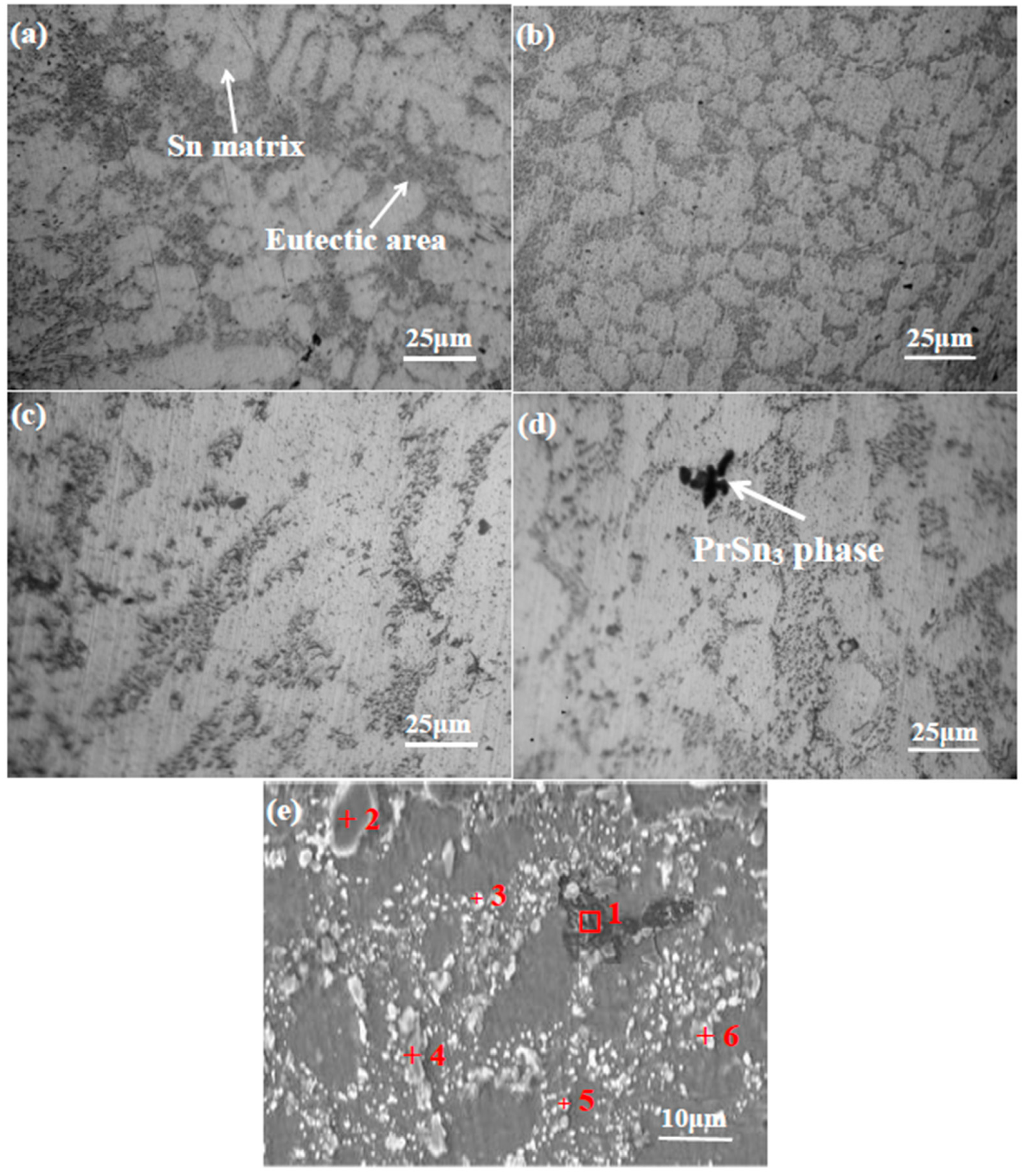
Figure 2.
Illustration of changes in IMCs in (a) SAC0307 solder and (b) SAC0307-0.05Pr solder during aging process.
Figure 2.
Illustration of changes in IMCs in (a) SAC0307 solder and (b) SAC0307-0.05Pr solder during aging process.
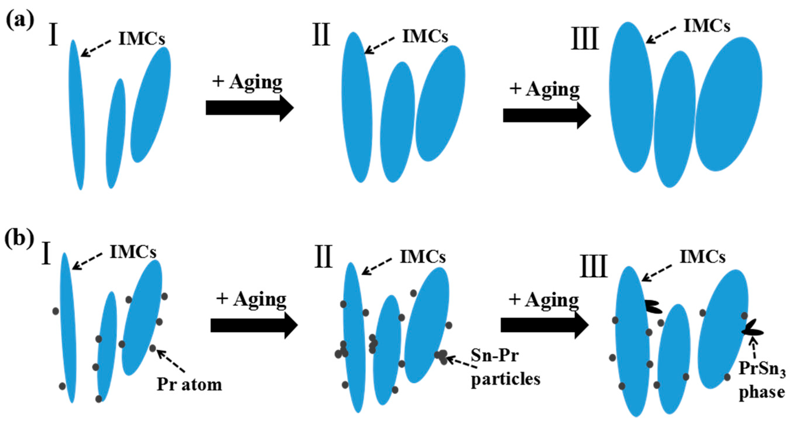
Figure 3.
SEM images of the interfacial morphology at SAC0307 solder/Cu interfaces aged at 150 °C for different hrs: (a) 72 h; (b) 240 h; (c) 528 h; (d) 840 h.
Figure 3.
SEM images of the interfacial morphology at SAC0307 solder/Cu interfaces aged at 150 °C for different hrs: (a) 72 h; (b) 240 h; (c) 528 h; (d) 840 h.
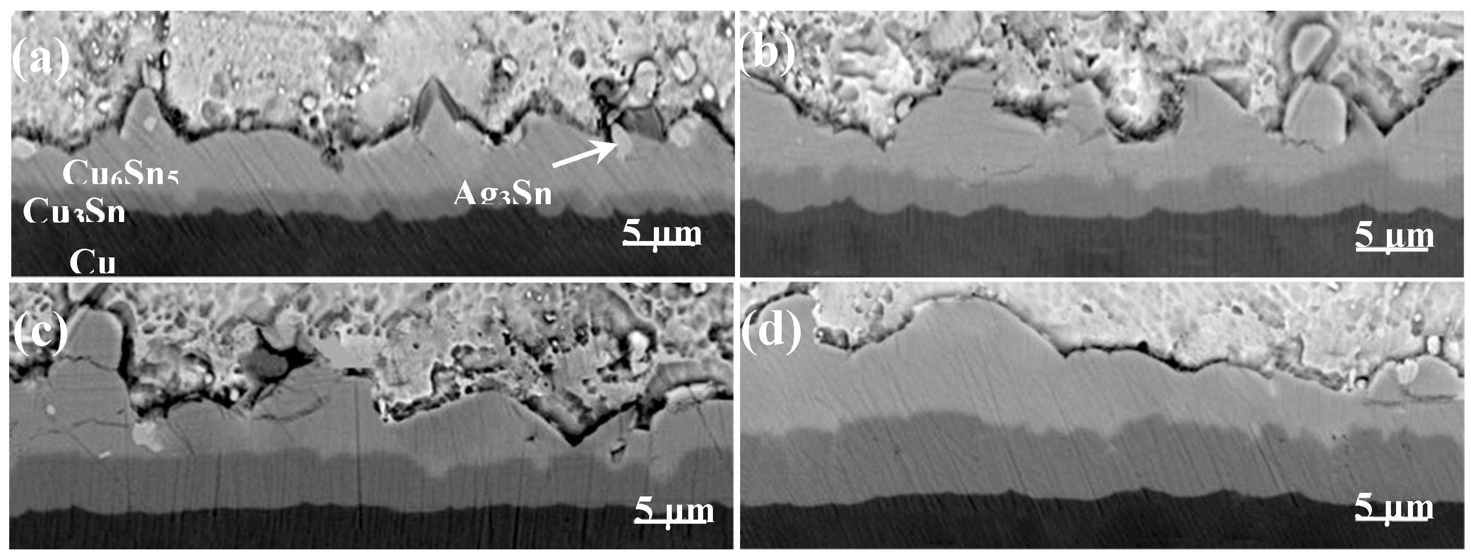
Figure 4.
SEM images of the interfacial morphology at SAC0307-0.05Pr solder/Cu interfaces aged at 150 °C for different hrs: (a) 72 h; (b) 240 h; (c) 528 h; (d) 840 h.
Figure 4.
SEM images of the interfacial morphology at SAC0307-0.05Pr solder/Cu interfaces aged at 150 °C for different hrs: (a) 72 h; (b) 240 h; (c) 528 h; (d) 840 h.
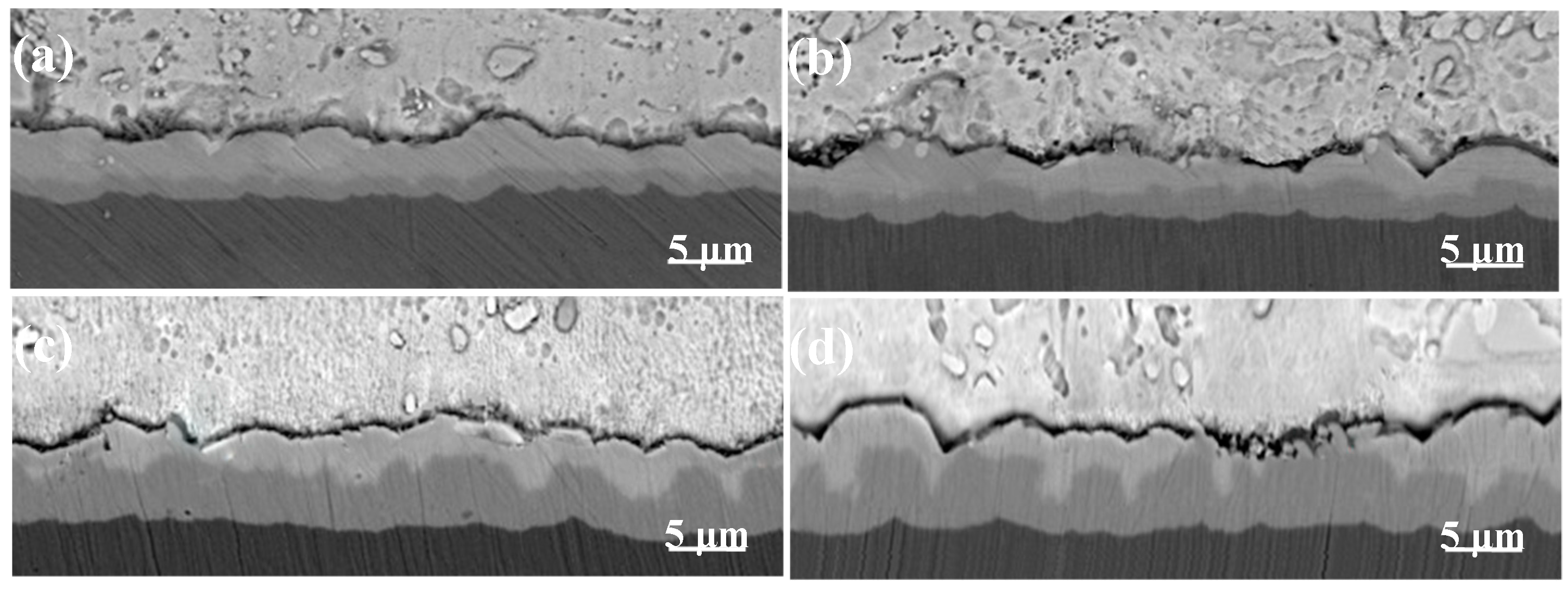
Figure 5.
Illustration of changes in interfacial IMCs at (a) SAC0307 solder/Cu interface and (b) SAC0307-0.05Pr solder/Cu interface during aging process.
Figure 5.
Illustration of changes in interfacial IMCs at (a) SAC0307 solder/Cu interface and (b) SAC0307-0.05Pr solder/Cu interface during aging process.
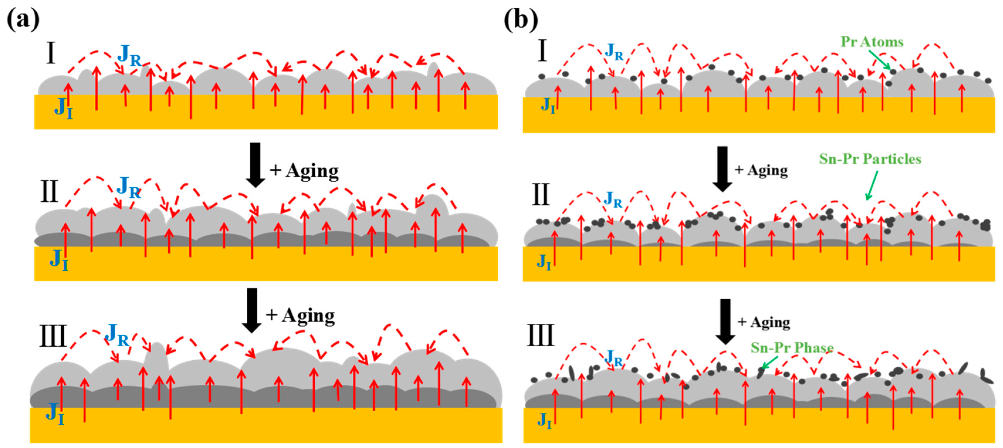
Figure 6.
Thickness of the (a) total interfacial IMC layers (IMLs) and (b) Cu3Sn IML at (a) SAC0307 solder/Cu interface and (b) SAC0307-0.05Pr solder/Cu interface aged at 150 °C for different hrs.
Figure 6.
Thickness of the (a) total interfacial IMC layers (IMLs) and (b) Cu3Sn IML at (a) SAC0307 solder/Cu interface and (b) SAC0307-0.05Pr solder/Cu interface aged at 150 °C for different hrs.
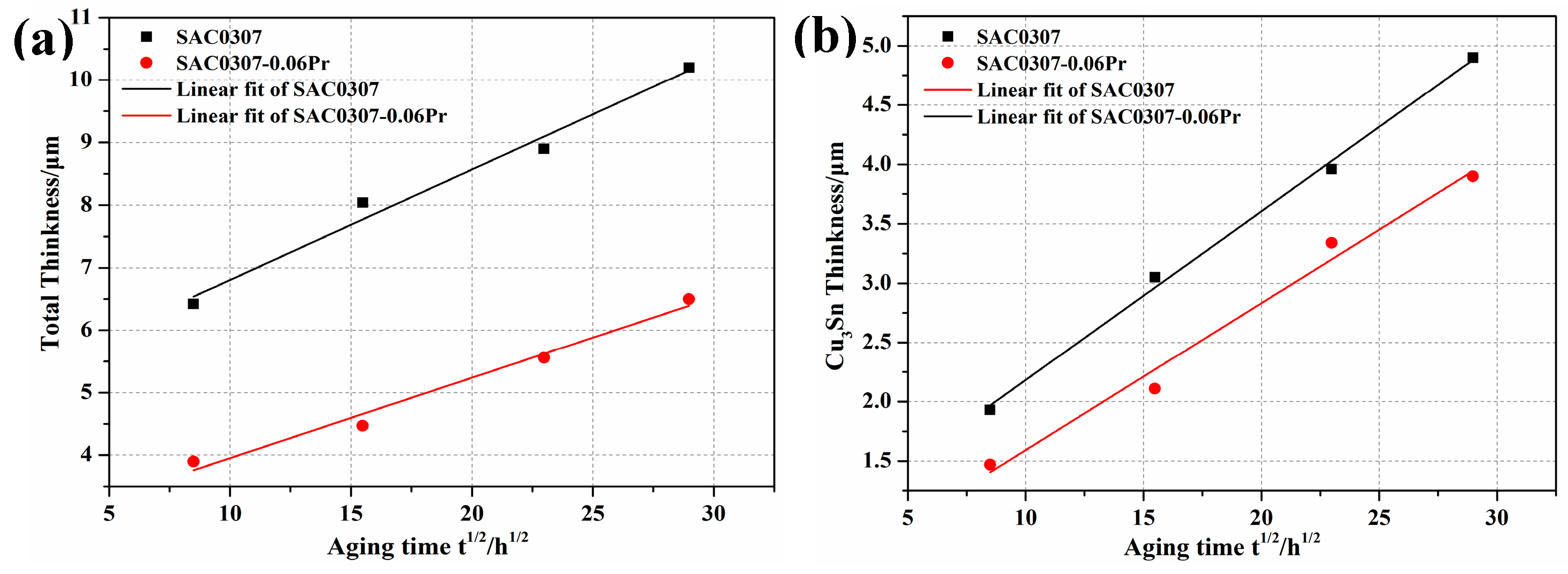
Figure 7.
(a) Illustration of shearing process; (b) Changes in shear strength at Sn-0.3Ag-0.7Cu solder/Cu and Sn-0.3Ag-0.7Cu-0.05Pr/Cu solder aged for different hrs.
Figure 7.
(a) Illustration of shearing process; (b) Changes in shear strength at Sn-0.3Ag-0.7Cu solder/Cu and Sn-0.3Ag-0.7Cu-0.05Pr/Cu solder aged for different hrs.

Figure 8.
Fracture morphology on the surface of (a) SAC0307/Cu, (b) SAC0307-0.05Pr/Cu interface, and (c) aged SAC0307/Cu interface at 150 °C for 840 h, (d) aged SAC0307-0.05Pr/Cu interface for 840 h, (e) EDS data of area A in Figure 8d.
Figure 8.
Fracture morphology on the surface of (a) SAC0307/Cu, (b) SAC0307-0.05Pr/Cu interface, and (c) aged SAC0307/Cu interface at 150 °C for 840 h, (d) aged SAC0307-0.05Pr/Cu interface for 840 h, (e) EDS data of area A in Figure 8d.

Table 1.
EDS analyzed results of related IMCs formed in the aged SAC0307-0.05Pr solder.
| Element Position | Sn | Ag | Cu | O | Pr | |||||
|---|---|---|---|---|---|---|---|---|---|---|
| Unit | wt.% | At.% | wt.% | At.% | wt.% | At.% | wt.% | At.% | wt.% | At.% |
| Point 1 | 35.68 | 22.35 | / | / | / | / | 10.57 | 49.23 | 53.75 | 28.42 |
| Point 2 | 58.40 | 42.26 | 2.41 | 1.92 | 38.43 | 51.71 | 0.76 | 4.11 | / | / |
| Point 3 | 26.80 | 23.8 | 71.98 | 70.43 | 0.45 | 0.75 | 0.77 | 5.02 | / | / |
| Point 4 | 55.95 | 40.11 | 2.80 | 2.21 | 40.57 | 54.08 | 0.68 | 3.6 | / | / |
| Point 5 | 30.68 | 27.69 | 68.59 | 68.21 | 0.15 | 0.26 | 0.58 | 3.84 | / | / |
| Point 6 | 31.03 | 28.44 | 68.32 | 69.01 | 0.37 | 0.63 | 0.28 | 1.92 | / | / |
Table 2.
Detailed thickness change with aged time at the interfaces of solders/Cu.
| Aging Hour (h) | 72 | 240 | 528 | 840 | |
|---|---|---|---|---|---|
| Solder | Interfacial IMC Layer | Thickness (μm) | |||
| SAC0307 | Total (Cu6Sn5+Cu3Sn) | 6.42 | 8.04 | 8.9 | 10.2 |
| Cu3Sn | 1.93 | 3.05 | 3.96 | 4.9 | |
| Cu6Sn5 | 4.49 | 4.99 | 4.94 | 5.3 | |
| SAC0307-0.05Pr | Total (Cu6Sn5+Cu3Sn) | 3.9 | 4.47 | 5.56 | 6.5 |
| Cu3Sn | 1.47 | 2.11 | 3.34 | 3.9 | |
| Cu6Sn5 | 2.43 | 2.36 | 2.22 | 2.6 | |
© 2019 by the authors. Licensee MDPI, Basel, Switzerland. This article is an open access article distributed under the terms and conditions of the Creative Commons Attribution (CC BY) license (http://creativecommons.org/licenses/by/4.0/).
Share and Cite
MDPI and ACS Style
Wu, J.; Xue, S.; Wang, J.; Huang, G. Effect of 0.05 wt.% Pr Addition on Microstructure and Shear Strength of Sn-0.3Ag-0.7Cu/Cu Solder Joint during the Thermal Aging Process. Appl. Sci. 2019, 9, 3590. https://doi.org/10.3390/app9173590
AMA Style
Wu J, Xue S, Wang J, Huang G. Effect of 0.05 wt.% Pr Addition on Microstructure and Shear Strength of Sn-0.3Ag-0.7Cu/Cu Solder Joint during the Thermal Aging Process. Applied Sciences. 2019; 9(17):3590. https://doi.org/10.3390/app9173590
Chicago/Turabian StyleWu, Jie, Songbai Xue, Jingwen Wang, and Guoqiang Huang. 2019. "Effect of 0.05 wt.% Pr Addition on Microstructure and Shear Strength of Sn-0.3Ag-0.7Cu/Cu Solder Joint during the Thermal Aging Process" Applied Sciences 9, no. 17: 3590. https://doi.org/10.3390/app9173590
Note that from the first issue of 2016, this journal uses article numbers instead of page numbers. See further details here.