Design and Experiment of Wideband Filters Based on Double-Layered Square-Loop Arrays in the F-Band
by
 , ,
, ,
Jun Yang
1 ,
,
Yang Yang
1,
Peng Wang
1,
Guangsheng Deng
1,
Fei Cai
1,
Hongbo Lu
1,2 and
Zhiping Yin
1,* 1
National Key Laboratory of Advanced Display Technology, Academy of Photoelectric Technology, Hefei University of Technology, Hefei 230009, China
2
Key Laboratory of Advanced Functional Materials and Devices of Anhui Province, School of Chemistry and Chemical Engineering, Hefei University of Technology, Hefei 230009, China
*
Author to whom correspondence should be addressed.
Appl. Sci. 2018, 8(9), 1669; https://doi.org/10.3390/app8091669
Submission received: 14 August 2018
/
Revised: 5 September 2018
/
Accepted: 12 September 2018
/
Published: 15 September 2018
Abstract
:Featured Application
The proposed filter in the article can be used in short millimeter wave communication system.
Abstract
We present a wideband metamaterial (MM) filter based on a metal-dielectric-metal (MDM) structure. The proposed structure consists of a quartz dielectric substrate and two metallic square-loop arrays, which were deposited on both surfaces of the substrate. The performance of the proposed design was numerically simulated by considering the angle of incidence. The surface current and electric field distributions were calculated for the two resonant frequencies to examine the intrinsic mechanism of the proposed filter. The transmittance of the structure for various oblique angles of incidence was also analyzed. It is generally challenging to completely align the two metallic layers due to limitations in the manufacturing process. Hence, the influence of periodic misalignment on wave propagation was studied. Furthermore, a prototype of the proposed structure was fabricated and the transmission spectra were measured. Simulation and experimental results reveal that our proposed filter can achieve wideband transmission in the F-band. This work is valuable for the design of broadband filters in millimeter and terahertz waves.
1. Introduction
In recent years, electromagnetic (EM) metamaterials have gained significant attention due to their unique physical properties, which are not commonly observed in natural materials. The unusual physical characteristics of metamaterials (MMs) lead to a variety of special electromagnetic effects, such as negative refractive index [1,2] and applications in invisible cloaks [3,4]. Other applications include filters [5,6], absorbers [7,8], modulators [9,10], and a number of others. As a basic wave control device, filters are widely used in imaging [11,12], sensing [13,14], and other fields [15]. Compared to traditional filters, a metamaterial filter has advantages of being ultra-thin, low cost, and light weight. Moreover, the operating frequencies of MM filters have been expanded from the microwave frequency range [16,17] to the THz range [18,19] and even to the optical range [20,21].
EM metamaterials typically consist of periodically patterned sub-wavelength metallic elements embedded within or on top of a dielectric substrate. The transmittance of subwavelength elements in a metal film is enhanced when the film is placed in a periodic array. Many kinds of MMs in single and multiple configurations have been proposed and studied in recent years. For example, transmittance and reflectance response of single layer consisted with a split-ring resonator (SRR) pair is studied at optical frequencies [22]. In one study [23], transmission spectra of terahertz pulses through periodic array of subwavelength holes with various hole widths are presented. However, the bandwidth and maximum transmission of the MMs with a single layer is restricted. Woo et al. [24] proposed a THz filter integrated with a subwavelength structured antireflection coating to reduce surface reflection loss and increase the bandwidth at frequencies ranging from 0.2 THz to 1.4 THz. Xiong et al. [25] proposed a thin, low-cost bandpass filter composed of double-layer tin foil with a hexagonal lattice array of circular holes and a 3-dB bandwidth is 0.20 THz from 0.81 to 1.01 THz. Bandpass filters were reported based on double-stacked metamaterial layers separated by an air gap with a 3-dB bandwidth of 78 GHz and 0.5 THz center frequency [26].
In this paper, we report a theoretical and experimental study on the transmission characteristics of continuous short millimeter waves through a metal-dielectric-metal (MDM) structure sandwiched between subwavelength periodic air square-loops. The normalized transmittance spectra through the two different structures were analyzed to explain the formation of two resonant peaks, f1 and f2. The surface current and electric field distributions of these resonant peaks were calculated to further understand the transmission mechanism. In addition, transmission of oblique incident waves through the structure and periodic misalignment were studied. A prototype of the proposed MDM structure was fabricated and the transmission spectra can be obtained with a vector network analyzer. The results from both simulations and experiments show that the proposed structure has a potential application as a wideband passband filter.
2. Design and Simulation
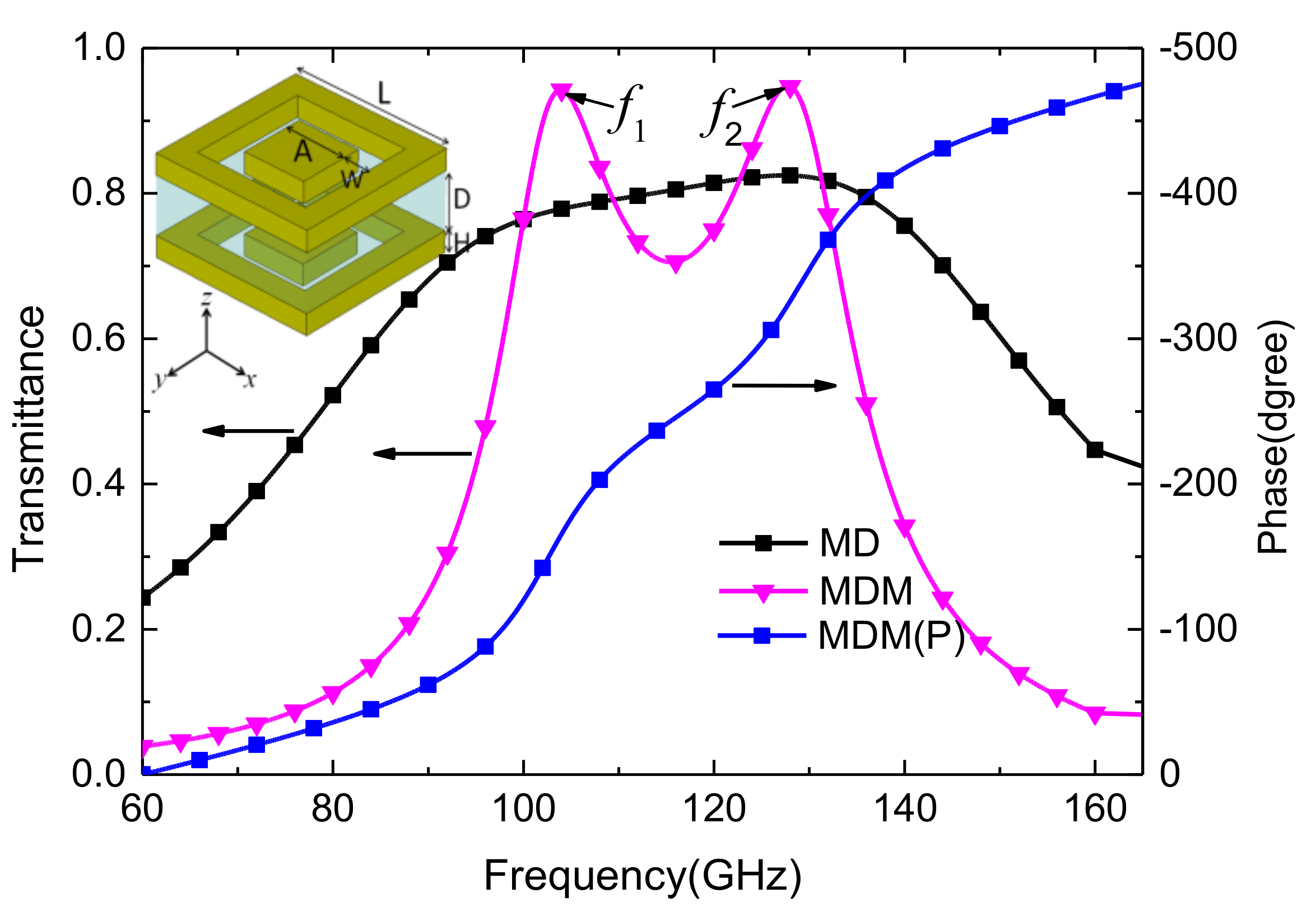
The unit cell of the proposed MDM structure is presented in Figure 1. The structure is composed of a dielectric layer and two metallic layers, which are deposited on both surfaces of the dielectric. The metallic layers are patterned with the same periodic subwavelength air square-loops. The specific parameters of the model are as follows: The lattice period L is 900 µm, internal square length A is 470 µm, loop width W is 40 µm, dielectric thickness D is 350 µm and metal thickness H is 1.5 µm. The electromagnetic performance of these structures has been analyzed and optimized using numerical finite-difference time-domain (FDTD) simulations while considering a conductivity of σ = 5.8 × 10⁷ S/m for copper. The substrates are formed on a 350 µm thick quartz plate with a relative dielectric constant and loss tangent of εQL = 3.78 and tanδQL = 0.002, respectively. A plane wave linearly polarized along the y-axis is normally incident on the structures and propagates along the negative z-axis direction. To better illustrate the performance, a metal-dielectric (MD) structure with only one metallic layer was also considered.
Figure 1 shows the transmittance spectra through the two proposed structures. For the MD structure, a maximum transmittance of 0.825 was obtained when an electromagnetic wave linearly polarized along the y-axis interacts with the structure. The phase changes on transmission of MDM structures also were shown in Figure 1. It is widely accepted that surface plasmons (SP) play crucial roles in the transmission of resonant electromagnetic waves [27]. The SP resonance originates from the excitation of collective oscillations of free electrons at the metal/dielectric interface termed as propagating surface plasmon (PSP) and localized surface plasmon (LSP). In the F-band, metals are regarded as almost perfect conductors and most energy of the SPs is owing to the electromagnetic wave localized at the air side. Thus, we call them surface waves (SWs) in this paper. For an array with a relatively thin metallic layer, SWs reside on both sides of the metal layer, which then couple via evanescent waves, thus leading to the formation of a transmission mode. For the MDM structure, when two metal interfaces are brought together (, where δ is the attenuation length of the SW), SWs around each interface couple together to produce two resonant peaks at f1 = 103.8 GHz and f2 = 127.45 GHz. It is evident that adding another metallic layer makes both resonant peaks more pronounced. The maximum in transmission is observed at the resonant frequencies for the MDM structure is formed by two complementary metasurfaces. The 3-dB bandwidth of proposed structure is 33.6 GHz in the 99.28–132.88 GHz frequency range, and both resonance peaks have maximum transmittance of approximately 0.945. Such a high transmittance indicates that the proposed structures possess potential in millimeter wave communication.
3. Analysis and Discussion
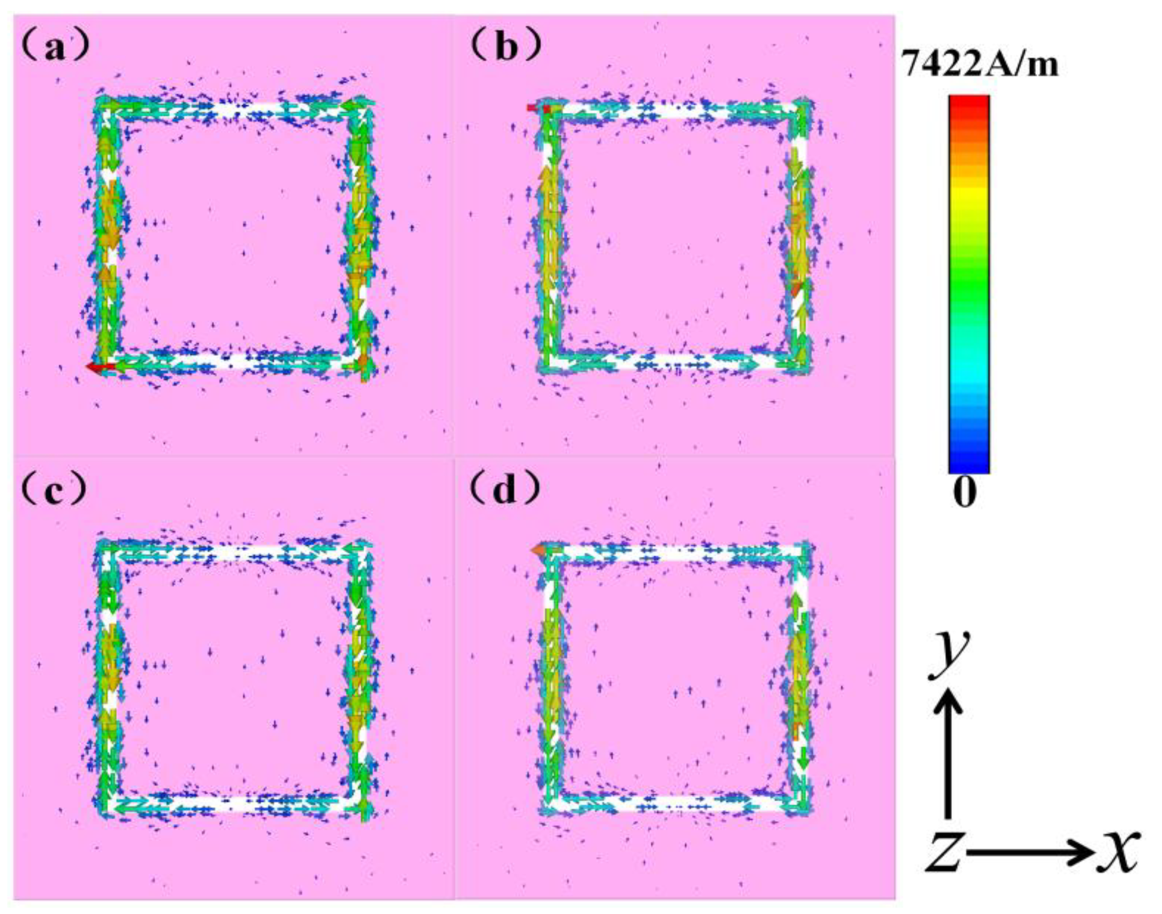
In order to examine the intrinsic mechanism of the MDM structure, the surface current and electric field distributions were calculated for the two resonant frequencies f1 and f2, and the obtained results are shown in Figure 2 and Figure 3. Figure 2 shows the surface current distributions in the first and second metal layers in f1 and f2, respectively. The surface currents along the square-loop mainly distribute at the edge of internal patch and external metal loop and flow parallel to the direction of the electric field vector of the incident wave, which excites a dipole response. One can see that the same resonant mode was excited from the surface current distribution of the two resonant frequencies in the first metal layer and excites two different resonant modes in the second metal layer with surface currents flowing in opposite directions.
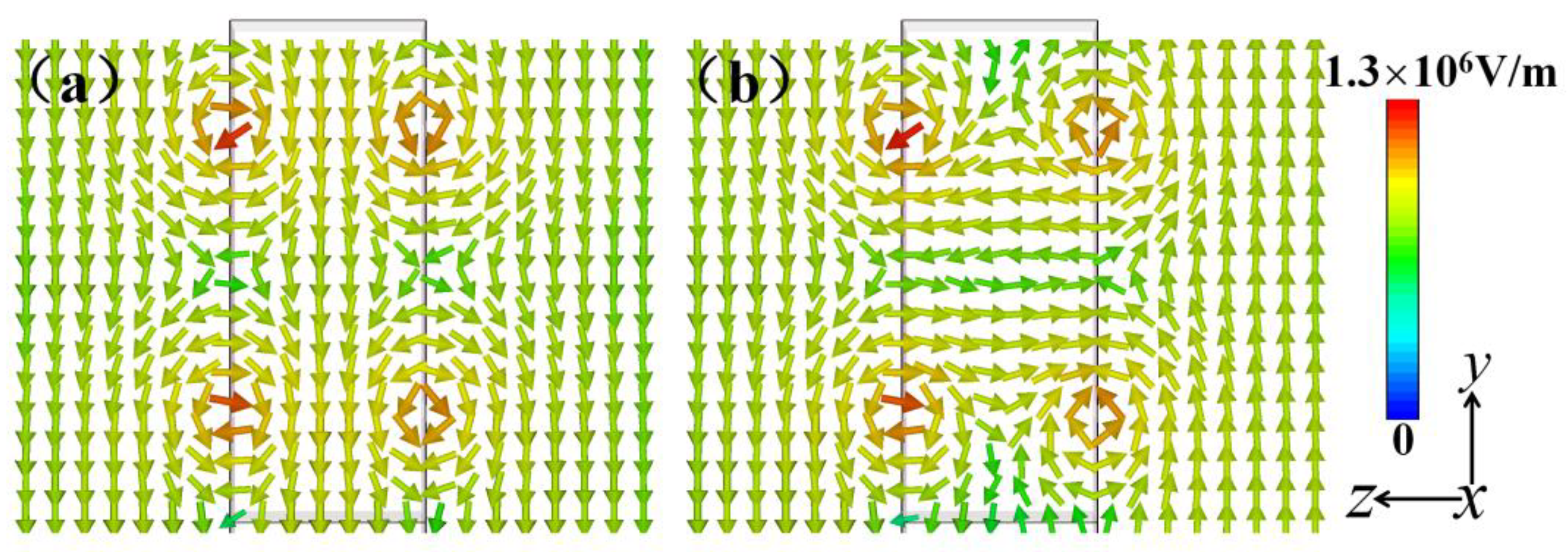
Figure 3 shows the electric field distributions in the y-z plane (x = L/2) for the two resonant frequencies f1 and f2. It is evident from Figure 3 that the incident electromagnetic wave propagates through the first metal layer and subsequently excites two different resonant modes with different electric field distributions in the second metal layer. However, the electric field intensity of the transmitted wave is approximately equal to the incident wave, indicating that the MDM structure possesses great transmission characteristics at both resonant frequencies.
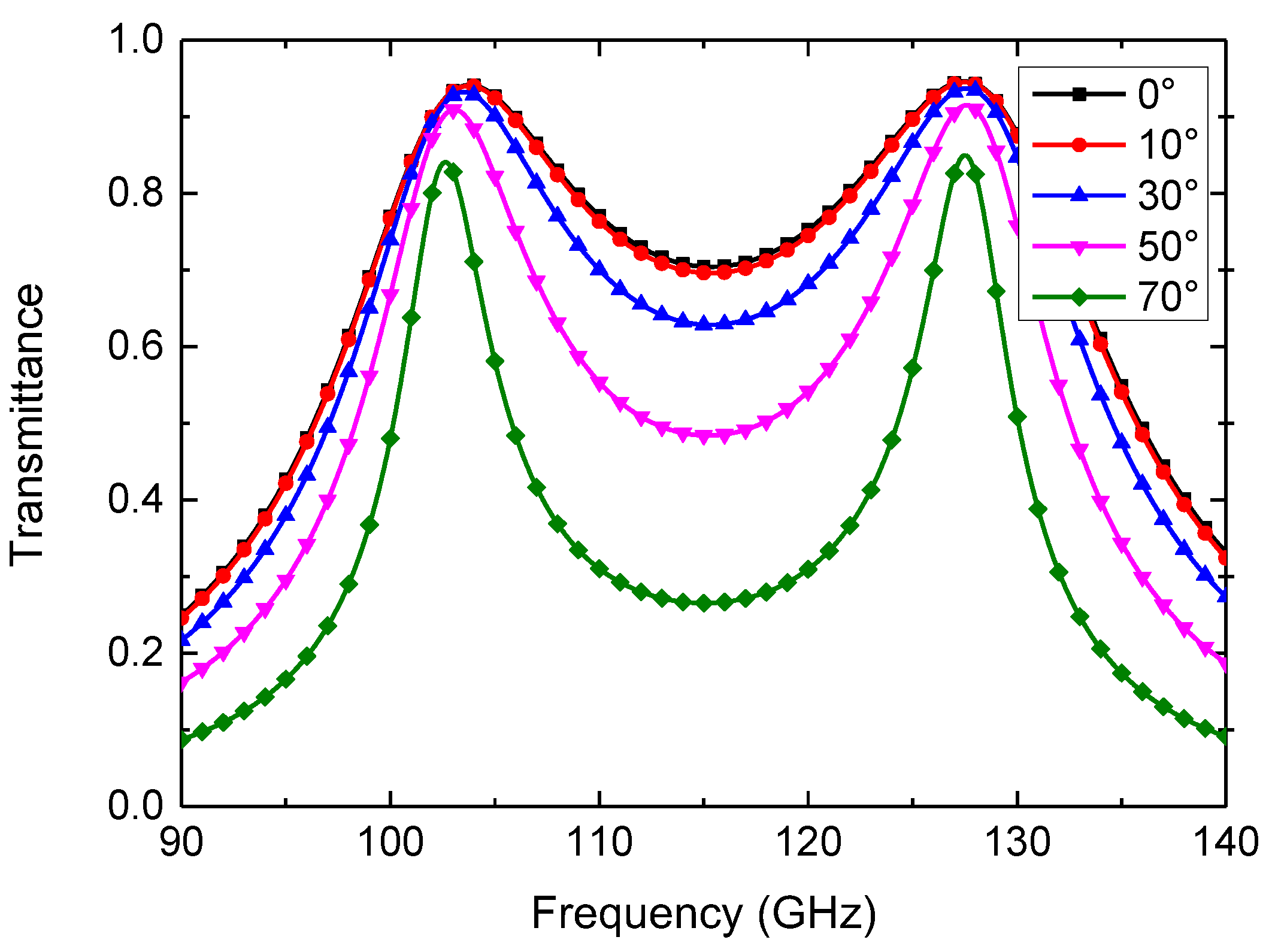
Transmittance through the proposed structure for various oblique angles of incidence is also shown in Figure 4. θ is the angle of incidence and is defined as the angle between k and the x-axis in the x-z plane. The electric field is parallel to the y-axis, whereas the wave propagation direction changes by varying θ. As shown in Figure 4, transmittance changes are not obvious as θ changes from 0° to 30°. If θ continues to increase the transmittance of the model decreases drastically. However, the minimum transmittance is slightly larger than 0.63 in the 98.84–132.77 GHz frequency range when the incident angle is 30°, which indicates broadband transmission.
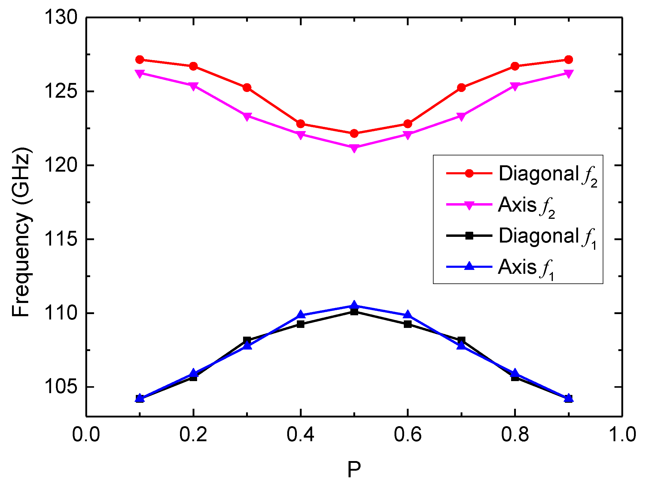
It is generally challenging to perfectly align the two metallic layers due to limitations in the manufacturing process. Hence, it is necessary to investigate how periodic misalignment influences wave propagation. Figure 5 shows how the two resonant peaks f1 and f2 vary for different P values ranging from 0.1 to 0.9 in two different directions (diagonal and axis directions), where P is defined as a measure of misalignment. For periodic misalignment along the diagonal direction, resonant peak f2 (red line) decreases and eventually reaches a minimum value of 122.15 GHz when P = 0.5. It then increases in a manner symmetrical to the first half of the curve when P varies from 0.6 to 0.9. This is because the proposed structure is symmetrical and periodic in both diagonal and axis directions. The value of f1 (black line) changes in an opposite manner compared to f2. For periodic misalignment along the axis direction, it is evident that variations in the two resonant peaks f1 and f2 are similar to those along the diagonal direction. The results shown in Figure 5 show that misalignment along both the diagonal and axis directions decreases the bandwidth of the MDM structure.
4. Experiment Results and Discussion
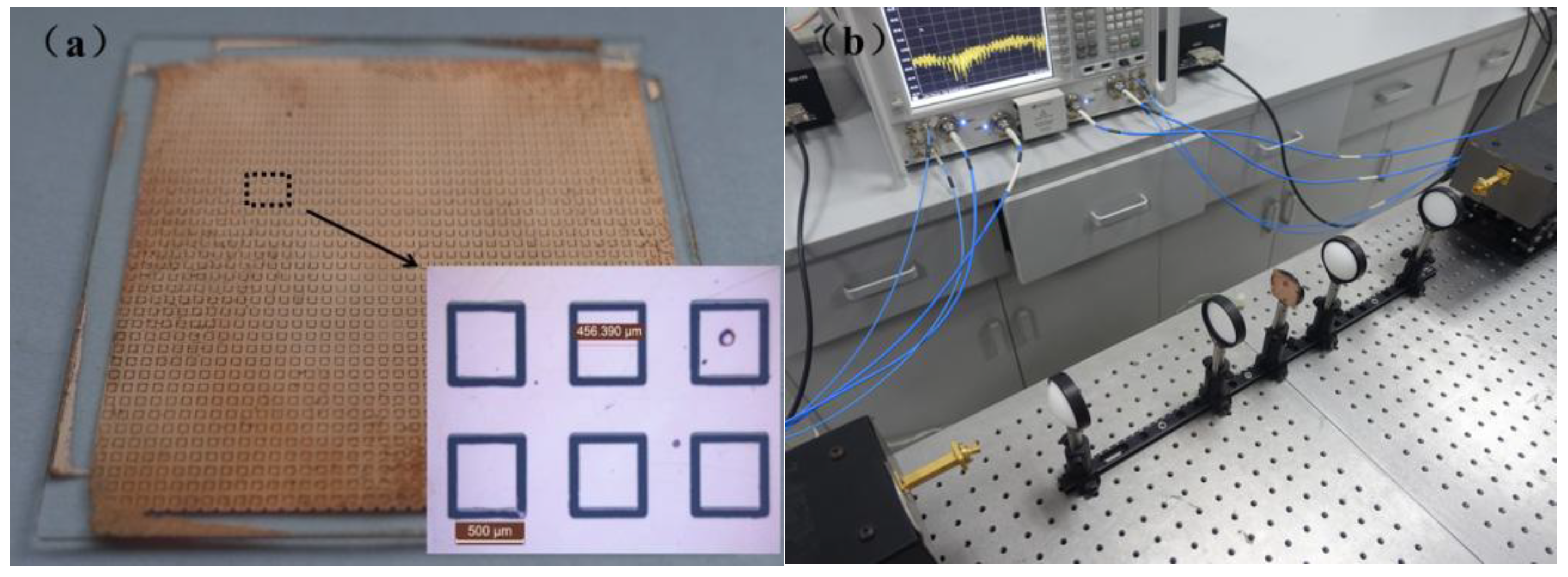
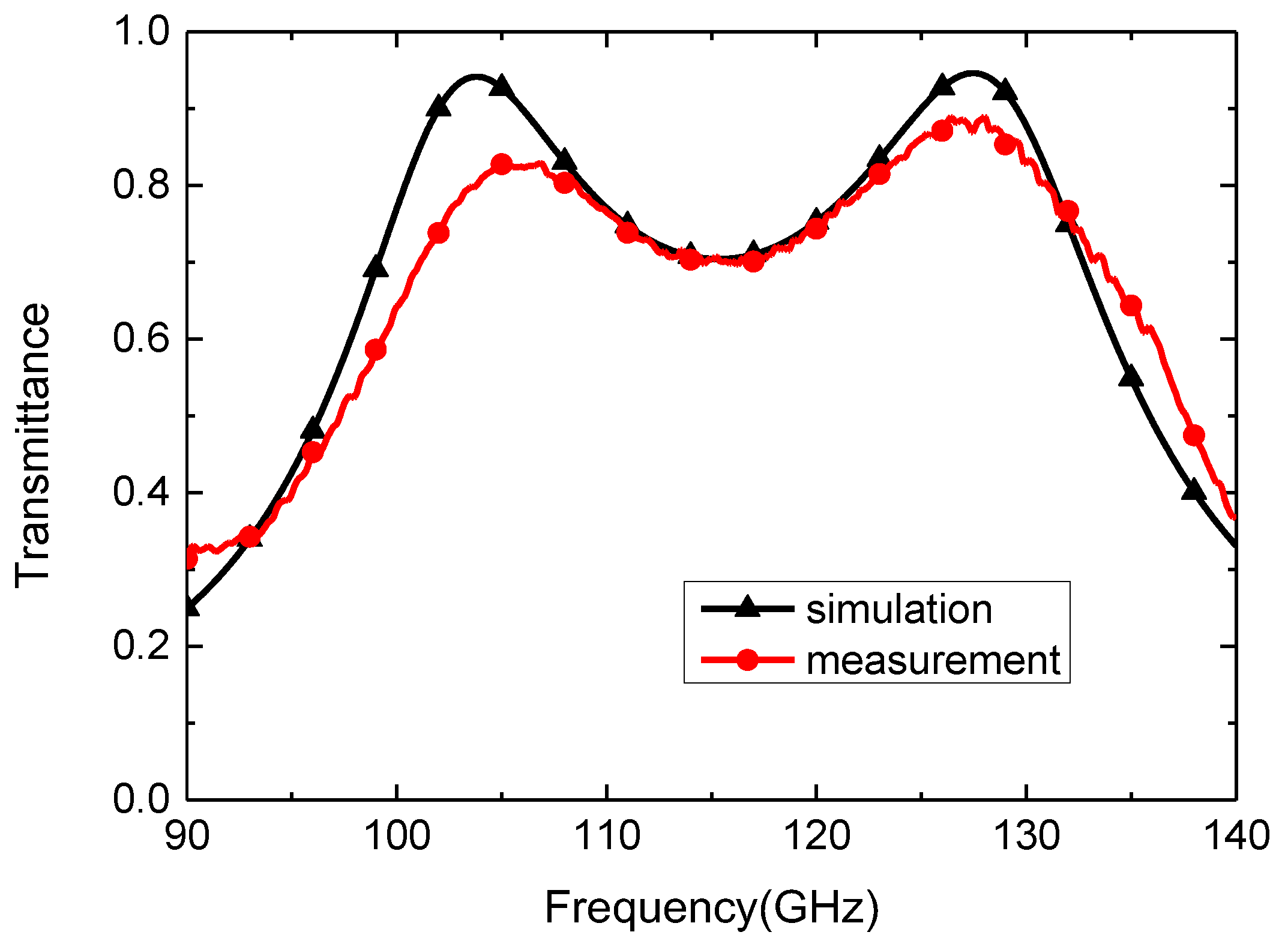
Based on the simulation results and analysis, the MDM structure with a quartz interlayer sandwiched between two metal layers was fabricated via ultraviolet light photoetching combined with wet etching. The process consists of vacuum copper plating, photoresist spin coating, exposure, development, and wet etching. The sample and a microscope image of several unit cells are shown in Figure 6a. The metallic layers were deposited on a 4 cm × 4 cm quartz plate. The measurement setup used in the experiment is shown in Figure 6b. One can see that the transfer characteristics were measured with a N5224A (Keysight Technologies, Inc., Santa Rosa, CA, USA) microwave network analyzer and a VDI WR8.0-VNAX (Virginia Diodes, Inc., Charlottesville, VA, USA) mixer module. Its available spectral range is from 90 GHz to 140 GHz. To accurately measure the transmission spectra, we used a lens to focus EM waves and reduce edge effects, as shown in Figure 6b. The simulated and experimental transmittance spectra are compared in Figure 7. One can see from Figure 7 that the experimental values of f1 and f2 are 105.81 GHz and 127.43 GHz with a transmittance of 0.83 and 0.89, respectively. The experimental results show that the resonant peaks are offset by approximately 1% and the amplitudes of the resonant peaks are approximately 10% lower than the simulation results. The 3-dB bandwidth determined from the experimental results is 32.1 GHz at frequencies ranging from 101.2–133.3 GHz. It should be pointed out that the relative dielectric constant of the quartz substrate is not constant over the F band, which causes the measured resonant frequencies to differ from the simulation results. Amplitude loss at these two resonant peaks could be due to the slightly oblique angles of incident waves through the lens platform. These should be the primary reason that the transmission spectra obtained in the measurements are slightly different from the transmission spectra calculated by FDTD method. Nevertheless, the simulation and experimental results qualitatively verify the validity of the design.
5. Conclusions
In summary, a compact wideband MM filter with a double-layered square-loop was proposed for transmission in the F-band. The transmission through the proposed filter was analyzed from the surface current and electric field distributions. In addition, transmission of electromagnetic waves through the structure at oblique incident angles and periodic misalignment of the structure were studied. The simulated results show that the proposed structure can provide high transmittance over a wide range of incident angles and values of periodic misalignment. A prototype was fabricated using ultraviolet light photoetching combined with wet etching. The experimental results show that the 3-dB bandwidth of proposed structure is 32.1 GHz in the 101.2–133.3 GHz frequency range and the maximum transmittance is 0.89 at 127.43 GHz. The measured transmission spectra show excellent agreement with the simulation results. Based on the presented results, one can conclude that the proposed filter, which is compact and ultra-broadband, has great potential applications in millimeter wave imaging, sensing and communication systems.
Author Contributions
Conceptualization and writing: review and editing, J.Y.; designed, measurement, writing: original draft, Y.Y.; fabricated, P.W.; data curation, G.D.; resources, F.C. and H.L; project administration, Z.Y.
Funding
This work is funded by the National Natural Science Foundation of China (Grant No.51607050) and the Fundamental Research Funds for the Central Universities (Grant No.JD2017JGPY0006).
Conflicts of Interest
The authors declare no conflicts of interest.
References
- Shalaev, V.M.; Cai, W.; Chettiar, U.K.; Yuan, H.-K.; Sarychev, A.K.; Drachev, V.P.; Kildishev, A.V. Negative index of refraction in optical metamaterials. Opt. Lett. 2005, 30, 3356–3358. [Google Scholar] [CrossRef] [PubMed]
- Smith, D.R.; Pendry, J.B.; Wiltshire, M.C.K. Metamaterials and negative refractive index. Science 2004, 305, 788–792. [Google Scholar] [CrossRef] [PubMed]
- Schurig, D.; Mock, J.J.; Justice, B.J.; Cummer, S.A.; Pendry, J.B.; Starr, A.F.; Smith, D.R. Metamaterial electromagnetic cloak at microwave frequencies. Science 2006, 314, 977–980. [Google Scholar] [CrossRef] [PubMed]
- Hao, J.M.; Yan, W.; Qiu, M. Super-reflection and cloaking based on zero index metamaterial. Appl. Phys. Lett. 2010, 96, 101109. [Google Scholar] [CrossRef] [Green Version]
- Sima, B.; Momeni Hasan Abadi, S.M.A.; Behdad, N. A reflective-type, quasi-optical metasurface filter. J. Appl. Phys. 2017, 122. [Google Scholar] [CrossRef]
- Yang, J.; Cheng, G.; Sun, L.; Chen, P.; Lin, L.; Liu, W.W. Tunable reflecting terahertz filter based on chirped metamaterial structure. Sci. Rep. 2016, 6, 38732. [Google Scholar] [CrossRef] [PubMed] [Green Version]
- Deng, G.; Yang, J.; Yin, Z. Broadband terahertz metamaterial absorber based on tantalum nitride. Appl. Opt. 2017, 56, 2449–2454. [Google Scholar] [CrossRef] [PubMed]
- Hossain, M.J.; Faruque, M.R.I.; Islam, M.T.; Mat, K.B. A new compact octagonal shape perfect metamaterial absorber for microwave applications. Appl. Sci. 2017, 7, 1263. [Google Scholar] [CrossRef]
- Zhang, X.-J.; Wu, X.; Xu, Y.-D. Controlling of the polarization states of electromagnetic waves using epsilon-near-zero metamaterials. Chin. Phys. Lett. 2017, 34, 084102. [Google Scholar] [CrossRef]
- Chen, H.-T.; Padilla, W.J.; Cich, M.J.; Azad, A.K.; Averitt, R.D.; Taylor, A.J. A metamaterial solid-state terahertz phase modulator. Nat. Photonics 2009, 3, 148. [Google Scholar] [CrossRef]
- Sleasman, T.; Imani, M.F.; Gollub, J.N.; Smith, D.R. Dynamic metamaterial aperture for microwave imaging. Appl. Phys. Lett. 2015, 107, 204104. [Google Scholar] [CrossRef]
- Yokogawa, S.; Burgos, S.P.; Atwater, H.A. Plasmonic color filters for CMOS image sensor applications. Nano Lett. 2012, 12, 4349–4354. [Google Scholar] [CrossRef] [PubMed]
- Chen, C.K.; Li, C.T.; Yen, T.J.; Lai, Y.C.; Chang, Y.T. A multi-functional plasmonic biosensor. Opt. Express 2010, 18, 9561–9569. [Google Scholar]
- O’Hara, J.F.; Singh, R.; Brener, I.; Smirnova, E.; Han, J.; Taylor, A.J.; Zhang, W. Thin-film sensing with planar terahertz metamaterials: sensitivity and limitations. Opt. Express 2008, 16, 1786–1795. [Google Scholar] [CrossRef] [PubMed]
- Renfors, M.; Siohan, P.; Farhang-Boroujeny, B.; Bader, F. Filter banks for next generation multicarrier wireless communications. EURASIP J. Adv. Signal Process. 2010, 2010, 324193. [Google Scholar] [CrossRef]
- Bi, K.; Zhu, W.; Lei, M.; Zhou, J. Magnetically tunable wideband microwave filter using ferrite-based metamaterials. Appl. Phys. Lett. 2015, 106, 173507. [Google Scholar] [CrossRef]
- Carver, J.; Reignault, V.; Gadot, F. Engineering of the metamaterial-based cut-band filter. Appl. Phys. A 2014, 117, 513–516. [Google Scholar] [CrossRef] [Green Version]
- Lin, Y.S.; Qian, Y.; Ma, F.; Liu, Z.; Kropelnicki, P.; Lee, C. Development of stress-induced curved actuators for a tunable THz filter based on double split-ring resonators. Appl. Phys. Lett. 2013, 102, 430. [Google Scholar] [CrossRef]
- Rao, L.; Yang, D.; Zhang, L.; Li, T.; Xia, S. Design and experimental verification of terahertz wideband filter based on double-layered metal hole arrays. Appl. Opt. 2012, 51, 912–916. [Google Scholar] [CrossRef] [PubMed]
- Si, G.; Zhao, Y.; Liu, H.; Teo, S.; Zhang, M.; Jun Huang, T.; Danner, A.J.; Teng, J. Annular aperture array based color filter. Appl. Phys. Lett. 2011, 99, 033105. [Google Scholar] [CrossRef]
- Zheludev, N.I.; Plum, E.; Fedotov, V.A. Metamaterial polarization spectral filter: Isolated transmission line at any prescribed wavelength. Appl. Phys. Lett. 2011, 99, 627. [Google Scholar] [CrossRef]
- Liu, N.; Kaiser, S.; Giessen, H. Magnetoinductive and electroinductive coupling in plasmonic metamaterial molecules. Adv. Mater. 2008, 20, 4521–4525. [Google Scholar] [CrossRef]
- Han, J.; Azad, A.K.; Gong, M.; Lu, X.; Zhang, W. Coupling between surface plasmons and nonresonant transmission in subwavelength holes at terahertz frequencies. Appl. Phys. Lett. 2007, 91, 071122. [Google Scholar] [CrossRef]
- Woo, J.M.; Kim, D.-S.; Kim, D.-J.; Jang, J.-H. Terahertz filter integrated with a subwavelength structured antireflection coating. AIP Adv. 2015, 5, 127238. [Google Scholar] [CrossRef] [Green Version]
- Xiong, R.H.; Li, J.S. Double-layer frequency selective surface for terahertz bandpass filter. J. Infrared Millim. Terahertz Waves 2018, 39, 1039–1046. [Google Scholar] [CrossRef]
- Zhu, Y.; Vegesna, S.; Kuryatkov, V.; Holtz, M.; Saed, M.; Bernussi, A.A. Terahertz bandpass filters using double-stacked metamaterial layers. Opt. Lett. 2012, 37, 296–298. [Google Scholar] [CrossRef] [PubMed]
- Xia, S.; Yang, D.; Li, T.; Liu, X.; Wang, J. Role of surface plasmon resonant modes in anomalous terahertz transmission through double-layer metal loop arrays. Opt. Lett. 2014, 39, 1270–1273. [Google Scholar] [CrossRef] [PubMed]
Figure 1.
Transmission spectra thourgh the metal−dielectric (MD) and metal−dielectric−metal (MDM) structures for a normally incident plane wave.
Figure 1.
Transmission spectra thourgh the metal−dielectric (MD) and metal−dielectric−metal (MDM) structures for a normally incident plane wave.

Figure 2.
Numerical simulation results. Distributions of the surface current for (a) the first metal layer and (b) second metal layer in f1 and (c) the first metal layer and (d) second metal layer in f2.
Figure 2.
Numerical simulation results. Distributions of the surface current for (a) the first metal layer and (b) second metal layer in f1 and (c) the first metal layer and (d) second metal layer in f2.

Figure 3.
Electric field distributions in the y-z plane (x = L/2) for (a) f1 and (b) f2.

Figure 4.
Oblique incidence response of the proposed structure.

Figure 5.
Resonant frequencies for various misalignments in the axial and diagonal directions.

Figure 6.
(a) Fabricated sample for the proposed structure and (b) experimental measurement setup.

Figure 7.
Simulation and measured transmittance of the proposed structure in the F-band.

© 2018 by the authors. Licensee MDPI, Basel, Switzerland. This article is an open access article distributed under the terms and conditions of the Creative Commons Attribution (CC BY) license (http://creativecommons.org/licenses/by/4.0/).
Share and Cite
MDPI and ACS Style
Yang, J.; Yang, Y.; Wang, P.; Deng, G.; Cai, F.; Lu, H.; Yin, Z. Design and Experiment of Wideband Filters Based on Double-Layered Square-Loop Arrays in the F-Band. Appl. Sci. 2018, 8, 1669. https://doi.org/10.3390/app8091669
AMA Style
Yang J, Yang Y, Wang P, Deng G, Cai F, Lu H, Yin Z. Design and Experiment of Wideband Filters Based on Double-Layered Square-Loop Arrays in the F-Band. Applied Sciences. 2018; 8(9):1669. https://doi.org/10.3390/app8091669
Chicago/Turabian StyleYang, Jun, Yang Yang, Peng Wang, Guangsheng Deng, Fei Cai, Hongbo Lu, and Zhiping Yin. 2018. "Design and Experiment of Wideband Filters Based on Double-Layered Square-Loop Arrays in the F-Band" Applied Sciences 8, no. 9: 1669. https://doi.org/10.3390/app8091669
Note that from the first issue of 2016, this journal uses article numbers instead of page numbers. See further details here.