Performance of InGaN/GaN Light Emitting Diodes with n-GaN Layer Embedded with SiO2 Nano-Particles


1
Department of Electronic Information Materials Engineering, Chonbuk National University, Jeonju 54896, Korea
2
Department of Optical Engineering, Kongju National University, Cheonan 31080, Korea
3
Department of Semiconductor Electronics and Semiconductor Physics, National University of Science and Technology MISiS, 119049 Moscow, Russia
4
Department of Materials Science and Engineering, Korea University, Seoul 02841, Korea
*
Authors to whom correspondence should be addressed.
Appl. Sci. 2018, 8(9), 1574; https://doi.org/10.3390/app8091574
Submission received: 9 August 2018
/
Revised: 29 August 2018
/
Accepted: 4 September 2018
/
Published: 6 September 2018
(This article belongs to the Special Issue Internal Quantum Efficiency of III-Nitride Light-Emitting Diodes)
Abstract
:We demonstrate high-performance InGaN/GaN blue light emitting diodes (LEDs) embedded with an air-void layer produced by a dry-etch of nano-pillars in an n-GaN layer grown on patterned sapphire substrate (PSS), filling the space between nano-pillars with SiO2 nano-particles (NPs) and subsequent epitaxial overgrowth. The structure exhibits enhanced output power compared to similarly grown reference conventional LED without the air-void layer. This change in growth procedure contributes to the increase of internal quantum efficiency (IQE) and light extraction efficiency (LEE) resulting in a 13.5% increase of light output. LEE is 2 times more affected than IQE in the modified structure. Simulation demonstrates that the main effect causing the LEE changes is due to the emitted light being confined within the upper space above the air-void layer and thus enhancing the light scattering by the SiO2 NPs and preferential light via front surface.
1. Introduction
Light emitting diodes (LEDs) and laser diodes are widely used optoelectronic devices, but many important problems still require solving. One of them is the strong lattice-mismatch during GaN growth on alien substrates [1,2]. In the case of the growth on conventional sapphire substrate, the threading dislocation (TD) density is as high as 108–1010 cm−2 [3]. As an option to decrease the TD density and increase the internal quantum efficiency (IQE), epitaxial lateral overgrowth (ELO) has been studied [4]. Another inherent problem of GaN-based LEDs is the low light extraction efficiency (LEE) due to the relatively low angle of total internal reflection (TIR) caused by the large difference between the refractive indices of air and GaN. This limits the extraction of light generated from the multi quantum well (MQW) of LEDs so that only a small portion of the light escapes towards the outside [5]. To enhance LEE, air void structures embedded in GaN-based LEDs have been studied, which is also useful to increase IQE and thus the external quantum efficiency (EQE) as a result [6,7,8].
IQE in InGaN/GaN blue LEDs has been remarkably improved and has been steadily approaching 100%, so that efforts on further improvement of EQE studies have to be focused on enhancing the LEE [9]. As an approach applicable to mass production, epoxy or silicone encapsulating has been preferred because the process is easy and simple, and readily meets the yield and cost requirements. When the encapsulation is applied on the outside of GaN devices which contact air, it is possible to make the refractive indices gap between the air and GaN smaller; and increase LEE because the refractive index of epoxy or silicone is between that of GaN and air [8]. Another approach to enhancing the LEE is by using textured surfaces, thus decreasing the total internal refraction (TIR) [10]. However, when the encapsulation is applied after texturing, the effect of roughening is considerably smothered. Thus, the combined effects of encapsulation and texturing do not simply add up, and the LEE enhancement produced by texturing is substantially handicapped by subsequent encapsulation [11,12]. Accordingly, adding an encapsulating layer after texturing in sequence is not an option to increase LEE and EQE.
As an alternative to processing the outward surface of LED, one can apply the texturing to inner LED layers. This will prevent negative interference between texturing and encapsulation by leaving the textured surface intact and not planarized by encapsulation applied to the front surface. As an example of successfully combining the two approaches, one can quote growth of GaN-based LED structures on patterned sapphire substrate (PSS) resulting, if properly designed, in about 60% increase of light output [13]. Slanted sides of the patterns in PSS deflect TDs laterally, resulting in bending out of TDs, decreasing the TD density toward the surface, and increasing IQE [14]. In addition, the slanted sides of patterns increase the light escape angle and thus decrease the effect of TIR. By this mechanism, photons, including photons which come out from the lower side of the MQW region, proceed toward the substrate and are reflected in a wider cone angle than the one observed for conventional sapphire substrate (CSS), which gives rise to increased LEE [15]. Thus, this paper adopts PSS as a platform for designing an epitaxial structure to maximize efficiency.
As a candidate of epitaxial structure to increase LEE, the air-void with hollow three-sided prism and cone shapes on CSS were demonstrated, resulting in scattering photons at the substrate and increasing LEE [16]. To form the air-void structures, SiO2 deposition on a substrate, patterning, ELO and wet etching were applied in sequence. This means that if PSS is selected as a substrate, the air-void shares the same location, the upper side of the substrate, with patterns of PSS. Because their dimension and shape are different, uniform selective ELO is hard to achieve. As another alternative, deposition of a layer of hollow silica nano-spheres was studied to decrease dislocation density, relax stress and increase LEE [17]. The silica nano-spheres were prepared on CSS, and ELO was processed in nano-scale. If PSS is applied with the silica nano-sphere together, uniform selective ELO is not possible too because of the different dimension and shape of PSS patterns and nano-spheres. In short, the air-voids and the silica nano-spheres on CSS are not compatible with PSS. Considering these aspects, it is required that the modified part of an epitaxial structure is positioned away from the upper side of the substrate in order for the former to effectively play a role in improving the crystalline quality and in scattering light.
LED structures overgrown on the GaN nano-pillar templates were demonstrated to show output power enhancement based on improved crystalline quality and additional light scattering [18,19,20,21]. We demonstrated the advanced LED structure on CSS with GaN nano-pillars filled with SiO2 nano-particles (NPs) to suppress dislocations propagating along the vertical growth direction from the bottom of air-void on CSS, resulting in ~300% increase in optical output power [3]. To maximize the light output, interlayer nano-pillar filled with SiO2 NPs in n-GaN [3] is applied in addition to using PSS for growth in this experiment. Texturing on the surface of LEDs, as an option to increase LEE, is excluded because the roughness caused by texturing would be buried with encapsulating by which the LEE increase by texturing could disappear. Therefore, the increased light output caused by this experiment could be treated as originating from within a device.
2. Experiment
In experiments, our suggested SiO2 NPs embedded PSS LEDs were compared with reference of a conventional PSS LED structure. First, a template of unintentionally doped u-GaN grown on PSS was prepared. A schematic illustration of the InGaN/GaN LED embedded with SiO2 NPs and process thereof are shown in Figure 1. With metal organic chemical vapor deposition (MOCVD), 3-μm-thick undoped GaN (u-GaN) films were grown on c-plane PSS in conventional way. To make nano-pillars in GaN film, a 100-nm-thick SiO2 layer was deposited as an interlayer on top of the u-GaN surface by plasma-enhanced chemical vapor deposition. With e-beam evaporation, a 10-nm-thick Ni layer was deposited on the SiO2 interlayer. To form the self-assembled Ni metal clusters, the Ni/SiO2/GaN samples were treated with rapid thermal annealing (RTA) under N2 flow at 850 °C for 1 min. Inductively coupled plasma (ICP) etching with the gases of O2 and CF4 was applied to pattern the SiO2 layer using the Ni nano-dots as an etch mask and then, the u-GaN was further etched down to 1.5 μm with Cl2 gas [22]. After that, the Ni nano-dots on SiO2, remaining on the tops of nano-pillars, were removed by buffered oxide etchant. As a result, a GaN template with vertically arranged nano-pillars was prepared. On the nano-pillar GaN template, the SiO2 NPs were deposited by spin coating (5000 rpm, 30 s). We used commercial colloidal SiO2 NPs with 100 nm diameter. This SiO2 embedded nano-pillar template was used for ELO overgrowth. The u-GaN templates grown on PSS without the nano-pillars (reference) were loaded at the same time. After well-coalesced GaN seed layer was formed on top of the nano-pillars, a Si-doped 3-μm-thick n-GaN layer, a multiquantum-well (MQW) region, and a 200-nm-thick Mg-doped p-GaN top contact layer were grown in sequence. The MQW region consisted of five undoped InGaN (2 nm)/GaN (10 nm) quantum wells.
The cross-section images of the SiO2 NP LED were obtained using a field emission scanning electron microscopy (FE-SEM). Room temperature photoluminescence (PL) mapping measurements were carried out with a 325 nm line of a 25 mW He-Cd laser as an excitation source. The current-voltage (I-V) and optical output (L-I) characteristics were measured by means of an on-wafer probing with indium contacts. The results were compared to those obtained from the reference sample—the growth conditions for both types of samples were the same, but for the fact of the presence of the nano-pillar region embedded with SiO2 NPs in the modified structure.
The experimentally observed performance increase is compared with the simulation result. Because the structure of this experiment and PSS are intended to increase LEE with different geometries, the simulation is planned to understand how to further increase the efficiency, which means geometrical differences are compatible and complementary to each other even when the functions are overlapped. Detailed conditions for the simulation are described in Appendix A.
3. Experimental Results
As a structure to be placed away from PSS within the outer surface of LEDs, the GaN nano-pillars and the air-void surrounding the nano-pillars filled with SiO2 NPs were fabricated as described above (Figure 1). To confirm the formation of nano-pillars and air-voids after regrowth, the cross-sectional images were obtained using FE-SEM. Figure 2a,b shows that the air-voids surrounding the nano-pillars were filled with the SiO2 NPs. With this configuration, GaN overgrowth begins on the upper part of each nano-pillar. The overgrowth expands laterally crossing the air-void and merges with adjacent laterally overgrown regions starting from neighboring nano-pillars. Figure 2c,d shows that GaN layer is formed on the top of the air-void and nano-pillars. This picture means that while the upper space of the air-void of Figure 2a,b was covered with GaN overgrowth, SiO2 NPs contributed to keep the shape and size of the air-void. As a result, the density of threading dislocations was diminished as shown in Appendix B. SiO2 NP LED shows 4 times lower TD density than that of the reference, which is a considerable improvement of the crystalline quality.
Figure 3 shows the performances of SiO2 NP LED compared to the reference LED. When 20 mA current is injected into the SiO2 NP LED and the reference LED, forward voltage is 2.84 V and 2.97 V, respectively (Figure 3a). The decrease of the forward voltage is considered as the result of the series resistance decrease caused by the TD decrease. This decrease in TD density comes in addition to the decrease of TD density produced by growth on the PSS which presents both in the reference and modified LED structures. From this perspective, the nano-pillar layer overcomes disadvantages of dislocation density control in PSS, resulting in better performance of the forward voltage. In relation to LEE, Figure 3b shows that the light output of the SiO2 NP LED is 13.5% higher than that of the reference LED.
Table 1 shows that the IQE of the SiO2 NP LED measured at 100 mA was 4.5% higher than that of the reference LED. The ABC model is well known to explain the rate of total recombination in LEDs. A, B, and C stands for Shockley–Read, radiative, and Auger recombination coefficient, respectively. The IQE was calculated with the ABC model under assumptions that the A and B coefficients were a function of current I, and C was much smaller than 10−30 (cm6·s−1) [23]. In the ABC model, the A coefficient is related to non-radiative recombination which describes the efficiency decrease due to non-radiative recombination on localized states. These defect levels can be due to localized states on dislocations and also to deep traps associated with point defects. However, in case of InGaN/GaN MQW LED, IQE increase was not proportional to TD decrease and localized. In composition fluctuation also affected the efficiency [24]. In addition, it has been observed that the density of deep Shockley–Hall–Read traps in modified structures was measurably lower than in reference structures [25]. Experiments with electron irradiation indicate that the increase in concentration of some of the detected deep traps correlated with the decrease of the EQE of irradiated LEDs [26].
Table 2 shows LEE calculated based on the light output data measured with integrating sphere system and the IQE of Table 1. The LEE increase is obtained with calculation using LEE = EQE/IQE. The experimental light output increment by % and IQE increment by % in comparison with the reference LED are assigned and the 8.6% of the LEE increment is obtained (1.135 (13.5%)/1.045 (4.5%) = 1.086 (8.6%)).
4. Simulation and Discussion
In the experiment, the air-void surrounding nano-pillars, the air-gap among SiO2 NPs, and SiO2 NPs themselves in the nano-pillar layer were designed to act as scattering centers together. To maximize light extraction performance, it is required to optimize conditions including the periodicity of the GaN pillars, the radius of the pillars, and the radius of SiO2 spheres of the structure demonstrated in this paper. As a basic consideration, to increase LEE toward the top surface, air-voids between the nano-pillars can be advantageous in terms of improved scattering than air-voids filled with SiO2 NPs because the refractive index gap between GaN and air is bigger than the one between GaN and SiO2, but only if the air-voids are as effective in ELO suppression of dislocation density as the voids filled with SiO2 (Appendix C). However, this is not the only reason to adopt air to act as a scattering center. There was a case of jointly using air and SiO2 at the same time that demonstrated effective light output enhancement with SiO2 nano-pattern layer which was placed over the air-void layer [27].
To understand a mechanism of LEE increase in the experiment, we numerically investigated the four types of LED structures by full three-dimensional (3-D) finite-difference time-domain (FDTD) method. The schematic structures for FDTD simulation are shown in the left of each four groups in Figure 4b; Type0 (conventional LED on CSS); Type1 (conventional LED on PSS, reference LED in the experiment); Type2 (SiO2 NP LED on CSS); Type3 (SiO2 NP LED on PSS in the experiment).
Figure 4a shows the top and bottom direction LEE, respectively, as a function of time after source excitations. In the case of the top direction LEE, the SiO2 NP LED on PSS shows the highest LEE during most of the time. In contrast, in the case of the bottom direction LEE, at initial time, the LEE of the conventional LED on PSS is higher than that of the SiO2 NP LED on PSS. However, the LEE of SiO2 NP LED on PSS shows the highest LEE after 0.7 ps. Figure 4b–e show the vertical cut-views of intensity distribution of the electric field at different times after source excitations in four different LEDs to illustrate the LEE increase mechanism of the experiment. According to Figure 4a, the top emission of Type3 is 10% higher than that of Type1 at the beginning and then converges to a level similar to Type1 later. It is considered that the increase at the beginning of Type3 is due to the structure playing two roles of confining and scattering photons within the upper volume above the nano-pillars. Photons of Type3 exist densely within about half size volume of Type1, which raises probability of scattering at the top of the nano-pillar layer and increases top emission. This analysis is matched with the simulation results shown in Figure 4b,e. It is worth noting that absorption of the materials including MQW was not considered in the simulation, therefore, the LEE might be saturated earlier than the simulation results. According to the field intensity distribution of Type3 at 3 ps in Figure 4e, the amount of photons in the volume below the nano-pillar layer becomes smaller than that in the volume above the nano-pillar layer, which leads us to conclude that light extraction toward the backside would decrease because the layer works as a light barrier. In this case, PSS on the bottom helps to increase light extraction toward the backside because the patterns of PSS work as textured surface, and sapphire itself functions as encapsulating layer with the refractive index 1.8 between GaN (2.5) and Air (1).
5. Conclusions
This study was intended to build a LED structure to achieve high efficiency considering encapsulation. The LEDs in this experiment adopted nano-pillars and an air-void filled with SiO2 NPs built in the GaN layer grown on the PSS within LEDs. The experimental results showed the increase of 13.5% light output with the increase of IQE. The simulation showed the nano-pillar layer working as a barrier to confine photons upwardly above the nano-pillar layer and also a reflector to scatter the crowded photons. The mechanism consisting of the two functions increased the light extraction efficiency to the front side.
Author Contributions
Writing-Original Draft Preparation with analysis, H.-S.Y.; FDTD simulation and writing-Review, J.-K.Y.; Writing-Review, A.Y.P.; Supervision and writing-Review, I.-H.L.
Funding
This research received no external funding.
Acknowledgments
This work was supported by National Research Foundation of Korea (NRF) funded by Ministry of Science and ICT (2017R1A2B3006141 and 2017R1A2B4012181). The work at NUST MISiS was supported in part by the Ministry of Education and Science of the Russian Federation in the framework of Increase Competitiveness Program of NUST «MISiS» (K2-2014-055).
Conflicts of Interest
The authors declare no conflict of interest.
Appendix A: 3-D FDTD Simulation Conditions
In 3-D FDTD simulation, the radius of the half sphere of PSS and its periodicity was fixed at 2 μm and 4.5 μm, respectively. Here, we assumed that the nano-pillars arranged periodically with the hexagonal lattice. According to the FE-SEM images as shown in Figure 2, the radius of the nano-pillar was 100 nm and the periodicity and the height of the pillar was set as 300 nm and 1 μm, respectively. Also, we assumed that the SiO2 spheres with the 50 nm radius were closely packed and filled in the air-void between the nano-pillars. The volume ratio of the materials in the nano-pillar layer is 57:31:68 (air:GaN:SiO2). The total thickness of the GaN layer including the nano-pillar was fixed at 12.1 μm and the center of the 1 μm thick nano-pillar was located at 5.6 μm from the top surface. In order to consider the limited computational memory, the lateral size of the total calculation domain is limited by 4.5 μm × 4.5 μm, the sapphire thickness was set as 2.5 μm. In consideration of the size of the fabricated sample, the periodic boundary conditions were used in the horizontal direction, and the perfectly matched layer was used as an absorbing layer in the vertical direction. The refractive indices of the GaN, SiO2, and sapphire were set as 2.5, 1.5, and 1.8, respectively. In order to consider the c-plane sapphire substrate, the 100 Ex and Ey dipole sources (l = 460 nm ± 30 nm) were generated at 100 nm from the top surface with random phase and position. The light extraction efficiency was obtained by dividing the output power flux toward top or bottom with the total dipole radiation power.
Appendix B: Dislocation Density Comparison
Figure A1.
Dislocation densities of reference LED ((a) ~4 × 10⁸/cm2) and SiO2 NP LED ((b) ~1 × 10⁸/cm2).
Figure A1.
Dislocation densities of reference LED ((a) ~4 × 10⁸/cm2) and SiO2 NP LED ((b) ~1 × 10⁸/cm2).

Appendix C: Light Extraction Efficiency Comparison
We calculated LEE of LED structure embedded with nano-pillars and air-void without SiO2 nano-particles (NPs) on PSS (air-void structure) as shown in Figure A2. In order to check the effect of SiO2, LEEs are plotted as a function of time with that of two different structures, conventional LED on PSS (PSS structure) and LED structure embedded with nano-pillars and air-void filled without SiO2 NPs on PSS (SiO2 structure). Figure A2 shows that LEE of the air-void structure is slightly higher than others. This is considered to be caused by the refractive index gap between GaN and air which is larger than that of SiO2 and air, and strong scattering to reflect light which is densely confined in the upper volume above the nano-pillars.
Figure A2.
Light extraction efficiencies of conventional structure on PSS (PSS structure), air-void without SiO2 nano-particles (NPs) on PSS (air-void structure), and air-void filled with SiO2 NPs on PSS (SiO2 structure) calculated with finite-difference time-domain (FDTD) method.
Figure A2.
Light extraction efficiencies of conventional structure on PSS (PSS structure), air-void without SiO2 nano-particles (NPs) on PSS (air-void structure), and air-void filled with SiO2 NPs on PSS (SiO2 structure) calculated with finite-difference time-domain (FDTD) method.

References
- DenBaars, S.P.; Feezell, D.; Kelchner, K.; Pimputkar, S.; Pan, C.; Tanaka, C.S.; Zhao, Y.; Pfaff, N.; Farrell, R.; Iza, M.; et al. Development of gallium-nitride-based light-emitting diodes (LEDs) and laser diodes for energy-efficient lighting and displays. Acta Mater. 2013, 61, 945–951. [Google Scholar] [CrossRef]
- Robertso, J. Diamond-like amorphous carbon. Mater. Sci. Eng. Rep. 2002, 37, 129–281. [Google Scholar] [CrossRef] [Green Version]
- Jeon, D.W.; Jang, L.W.; Cho, H.S.; Kwon, K.S.; Dong, M.J.; Polyakov, A.Y.; Ju, J.W.; Chung, T.H.; Baek, J.H.; Lee, I.-H. Enhanced optical output performance in InGaN/GaN light-emitting diode embedded with SiO2 nanoparticles. Opt. Express 2014, 22, 21454–21459. [Google Scholar] [CrossRef] [PubMed]
- Kim, B.; Jang, S.; Kim, S.; Kim, Y.; Lee, J.; Byun, D. Epitaxial Lateral Overgrowth of GaN on Sapphire Substrate Using High-Dose N+-Ion-Implantation. J. Electrochem. Soc. 2010, 157, H1132–H1134. [Google Scholar] [CrossRef]
- Son, J.H.; Kim, J.U.; Song, Y.H.; Kim, B.J.; Ryu, C.J.; Lee, J.L. Design Rule of Nanostructures in Light-Emitting Diodes for Complete Elimination of Total Internal Reflection. Adv. Mater. 2012, 24, 2259–2262. [Google Scholar] [CrossRef] [PubMed]
- Kim, H.G.; Kim, H.K.; Kim, H.Y.; Ryu, J.H.; Kang, J.H.; Han, N.; Uthirakumar, P.; Hong, C.H. Impact of two-floor air prism arrays as an embedded reflector for enhancing the output power of InGaN/GaN light emitting diodes. Appl. Phys. Lett. 2009, 95, 221110. [Google Scholar] [CrossRef]
- Cho, C.Y.; Kwon, M.K.; Park, I.K.; Hong, S.H.; Kim, J.J.; Park, S.E.; Kim, S.T.; Park, S.J. High-efficiency light-emitting diode with air voids embedded in lateral epitaxially overgrown GaN using a metal mask. Opt. Express 2011, 19, A943–A948. [Google Scholar] [CrossRef] [PubMed]
- Park, Y.J.; Kang, J.H.; Kim, H.Y.; Lysak, V.V.; Chandramohan, S.; Ryu, J.H.; Kim, H.K.; Han, N.; Jeong, H.; Jeong, M.S.; et al. Enhanced light emission in blue light-emitting diodes by multiple Mie scattering from embedded silica nanosphere stacking layers. Opt. Express 2011, 19, 23429–23435. [Google Scholar] [CrossRef] [PubMed]
- Fujii, T.; Gao, Y.; Sharma, R.; Hu, E.L.; DenBaars, S.P.; Nakamura, S. Increase in the extraction efficiency of GaN-based light-emitting diodes via surface roughening. Appl. Phys. Lett. 2004, 84, 855. [Google Scholar] [CrossRef]
- Pan, J.W.; Wang, C.S. Light extraction efficiency of GaN-based LED with pyramid texture by using ray path analysis. Opt. Express 2012, 20, A630–A640. [Google Scholar] [CrossRef] [PubMed]
- Lee, T.X.; Gao, K.F.; Chien, W.T.; Sun, C.C. Light extraction analysis of GaN-based light-emitting diodes with surface texture and/or patterned substrate. Opt. Express 2007, 15, 6670–6676. [Google Scholar] [CrossRef] [PubMed]
- Kang, J.H.; Ryu, J.H.; Kim, H.K.; Kim, H.Y.; Han, N.; Park, Y.J.; Uthirakumar, P.; Hong, C.H. Comparison of various surface textured layer in InGaN LEDs for high light extraction efficiency. Opt. Express 2011, 19, 3637–3647. [Google Scholar] [CrossRef] [PubMed]
- Cheng, J.H.; Wu, Y.C.S.; Liao, W.C.; Lin, B.W. Improved crystal quality and performance of GaN-based light-emitting diodes by decreasing the slanted angle of patterned sapphire. Appl. Phys. Lett. 2010, 96, 051109. [Google Scholar] [CrossRef]
- Xu, S.R.; Li, P.X.; Jiang, J.C.T.; Ma, J.J.; Lin, Z.Y.; Hao, Y. Threading dislocation annihilation in the GaN layer on cone patterned sapphire substrate. J. Alloy. Compd. 2014, 614, 360–363. [Google Scholar] [CrossRef]
- Ko, D.; Yoon, J.; Seo, J. Patterned substrates enhance LED light extraction. LEDs Magazine, 22 July 2014; 53–58. [Google Scholar]
- Lysak, V.V.; Kang, J.H.; Hong, C.H. Conical air prism arrays as an embedded reflector for high efficient InGaN/GaN light emitting diodes. Appl. Phys. Lett. 2013, 102, 061114. [Google Scholar] [CrossRef]
- Kim, J.; Woo, H.; Joo, K.; Tae, S.; Park, J.; Moon, D.; Park, S.H.; Jang, J.; Cho, Y.; Park, J.; et al. Less strained and more efficient GaN light-emitting diodes with embedded silica hollow nanospheres. Sci. Rep. 2013, 3, 3201. [Google Scholar] [CrossRef] [PubMed] [Green Version]
- Chiu, C.H.; Yen, H.H.; Chao, C.L.; Li, Z.Y.; Yu, P.; Kuo, H.C.; Lu, T.C.; Wang, S.C.; Lau, K.M.; Cheng, S.J. Nanoscale epitaxial lateral overgrowth of GaN-based light-emitting diodes on a SiO2 nanorod-array patterned sapphire template. Appl. Phys. Lett. 2008, 93, 081108. [Google Scholar] [CrossRef]
- Wuu, D.S.; Wang, W.K.; Wen, K.S.; Huang, S.C.; Lin, S.H.; Huang, S.Y.; Lin, C.F. Defect reduction and efficiency improvement of near-ultraviolet emitters via laterally overgrown GaN on a GaN/patterned sapphire template. Appl. Phys. Lett. 2006, 89, 161105. [Google Scholar] [CrossRef]
- Park, J.M.; Oh, J.K.; Kwon, K.W.; Kim, Y.H.; Jo, S.S.; Lee, J.K.; Ryu, S.W. Improved light output of photonic crystal light-emitting diode fabricated by anodized aluminum oxide nano-patterns. IEEE Photon. Technol. Lett. 2008, 20, 321–323. [Google Scholar] [CrossRef]
- Kuo, C.H.; Chang, L.C.; Chou, H.M. Current spreading improvement in GaN-based light-emitting diode grown on nano-rod GaN template. IEEE Photon. Technol. Lett. 2012, 24, 608–610. [Google Scholar] [CrossRef]
- Jeon, D.W.; Choi, W.M.; Shin, H.J.; Yoon, S.M.; Choi, J.Y.; Jang, L.W.; Lee, I.-H. Nanopillar InGaN/GaN light emitting diodes integrated with homogeneous multilayer grapheme electrodes. J. Mater. Chem. 2011, 21, 17688–17692. [Google Scholar] [CrossRef]
- Shim, J.I.; Ryu, H.Y. Explanation of the efficiency droop in InGaN multiple quantum well light-emitting diodes by the reduced radiative recombination probability. In Proceedings of the 2010 SPIE Photonic West, San Francisco, CA, USA, 23–28 January 2010; pp. 7617–7619. [Google Scholar] [CrossRef]
- Mukai, T.; Nakamura, S. Ultraviolet InGaN and GaN Single-Quantum-Well-Structure Light-Emitting Diodes Grown on Epitaxially Laterally Overgrown GaN Substrates. J. Appl. Phys. 1999, 38, 5735. [Google Scholar] [CrossRef]
- Polyakov, A.Y.; Smirnov, N.B.; Yakimov, E.B.; Cho, H.S.; Baek, J.H.; Turutin, A.V.; Shemerov, I.V.; Kondratyev, E.S.; Lee, I.-H. Deep Electron Traps Responsible for Higher Quantum Efficiency in Improved GaN/InGaN Light Emitting Diodes Embedded with SiO2 Nanoparticles. ECS Solid State Sci. Technol. 2016, 5, Q274–Q277. [Google Scholar] [CrossRef]
- Lee, I.-H.; Polyakov, A.Y.; Smirnov, N.B.; Shchemerov, I.V.; Lagov, P.B.; Zinov’ev, R.A.; Yakimov, E.B.; Shcherbachev, K.D.; Pearton, S.J. Point defects controlling non-radiative recombination in GaN blue light emitting diodes: Insights from radiation damage experiments. J. Appl. Phys. 2017, 122, 115704. [Google Scholar] [CrossRef]
- Chiu, C.H.; Lin, C.C.; Han, H.V.; Liu, C.Y.; Chen, Y.H.; Lan, Y.P.; Yu, P.; Kuo, H.C.; Lu, T.C.; Wang, S.C.; et al. High efficiency GaN-based light-emitting diodes with embedded air voids/SiO2 nanomasks. Nanotechnology 2012, 23, 045303. [Google Scholar] [CrossRef] [PubMed]
Figure 1.
(a) GaN light emitting diode (LED) structure consisting of nano-pillars and air-void filled with SiO2 nano-particles (NPs) formed on patterned sapphire substrate (PSS). (b) Schematic illustration of the process flow to use Ni dots as a mask to form nano-pillars and fill air-void with SiO2 NPs, and regrow GaN. ICP: inductively coupled plasma; MQW: multi quantum well.
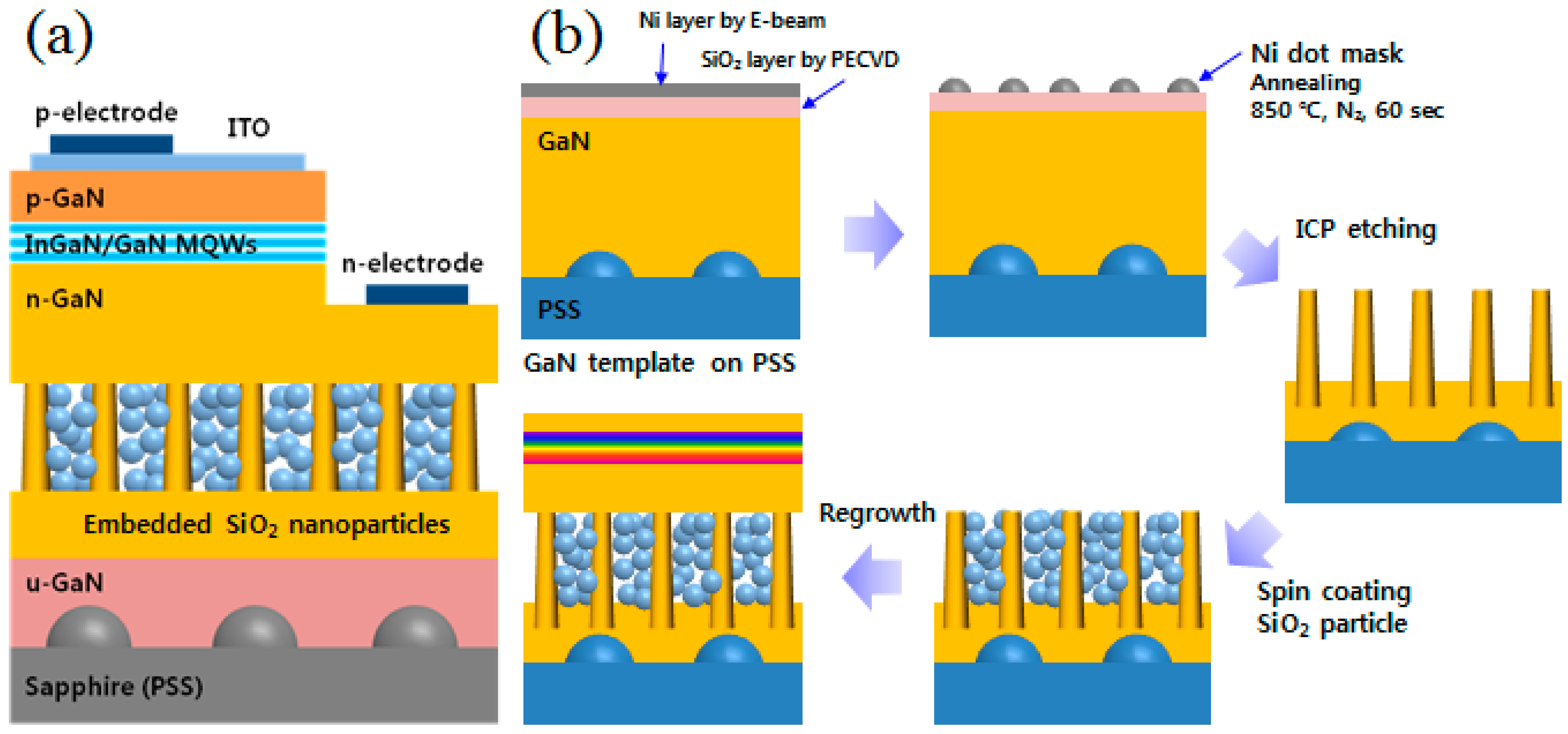
Figure 2.
(a) Tilted field emission scanning electron microscopy (FE-SEM) image of the SiO2 nano-particles (NPs) among nano-pillars. (b) Zoomed-in image to show the NPs clearly in air-void. (c) FE-SEM image of cross-section of the regrown GaN layer with air-voids and nano-pillars. (d) Close-up image of cross-section of revealed SiO2 NPs filling the air-voids on the left.
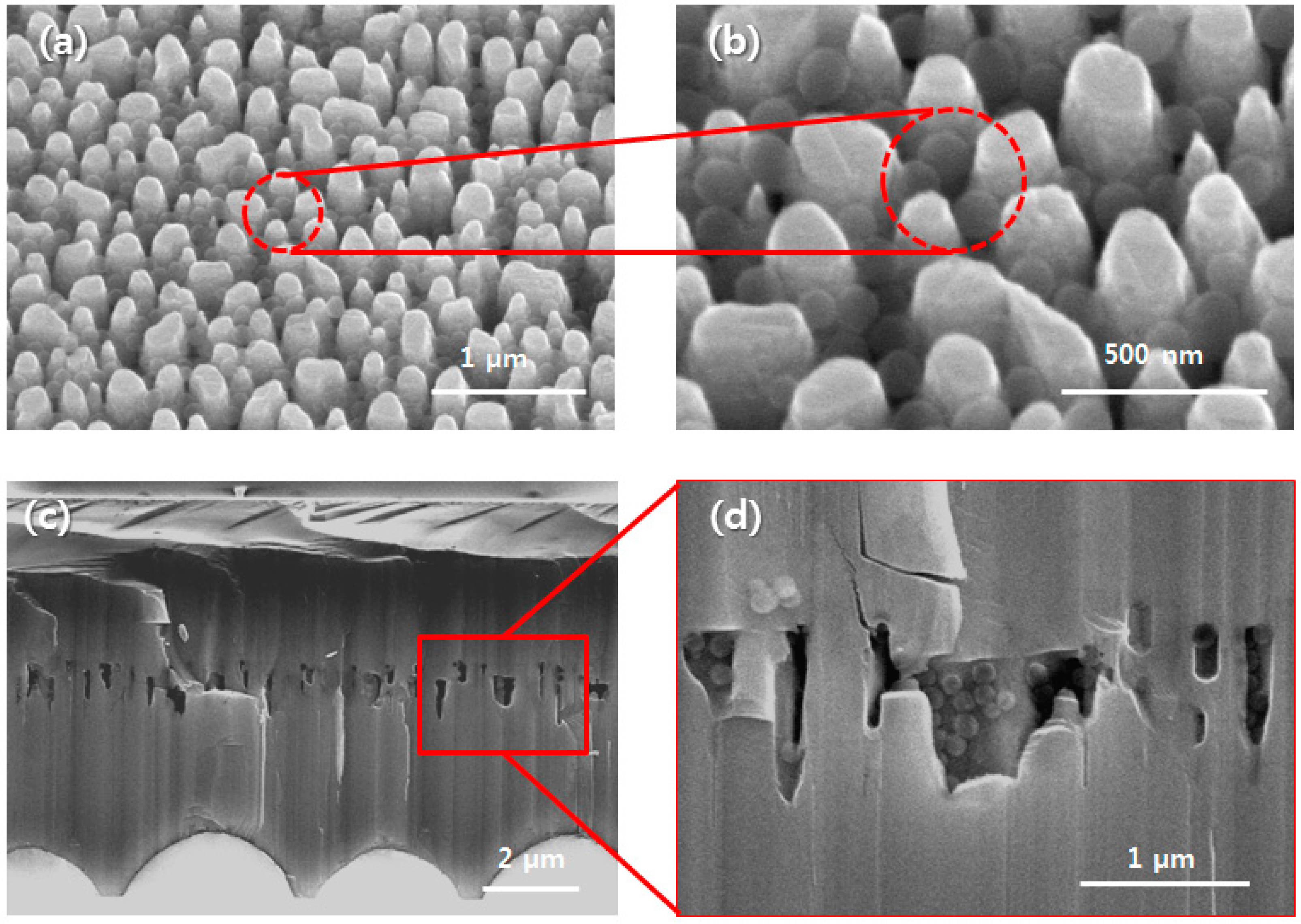
Figure 3.
Device characterizations of (a) current-voltage (I-V) curve and (b) optical output (L-I) curve (Experimental result).
Figure 3.
Device characterizations of (a) current-voltage (I-V) curve and (b) optical output (L-I) curve (Experimental result).
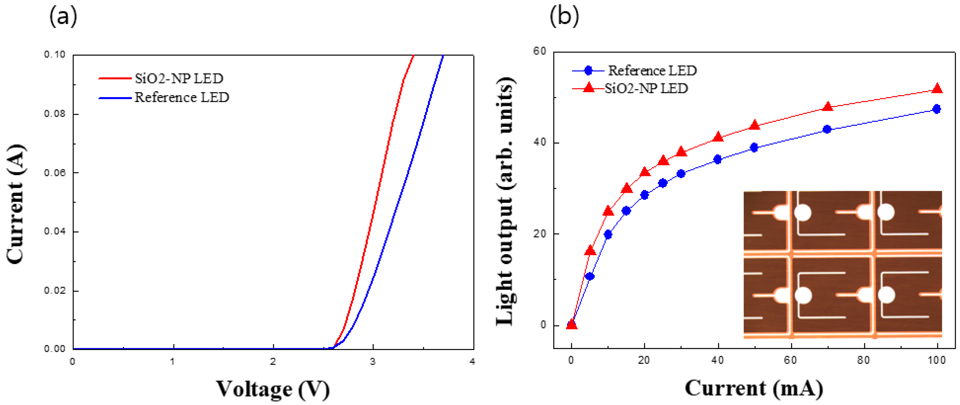
Figure 4.
(Simulation data) (a) Top and bottom direction light extraction efficiency (LEE) of four types as a function of time after source excitation. (b–e) Cut-views of intensity distributions of the electric field at different times after source excitations shown at the bottom. (b) Reference (c) PSS (d) SiO2, and (e) PSS + SiO2. The dotted lines indicate the boundary of the materials.


Table 1.
Internal quantum efficiency (IQE) of the SiO2 nano-particle (NP) light emitting diode (LED) and the reference LED (Experimental result).
Table 1.
Internal quantum efficiency (IQE) of the SiO2 nano-particle (NP) light emitting diode (LED) and the reference LED (Experimental result).
| IQE [%] a) | At 20 mA | At 100 mA |
|---|---|---|
| Reference LED | 88.7 | 84 |
| SiO2 NP LED | 91.2 | 87.8 |
a) (average, chip on wafer).
Table 2.
Calculated light extraction efficiency (LEE) based on the light output data (Experimental result).
Table 2.
Calculated light extraction efficiency (LEE) based on the light output data (Experimental result).
| Light Output Increase a) | 13.5% |
| IQE Increase | 4.5% |
| LEE Increase | 8.6% |
a) (at 100 mA, measured with integrating sphere).
© 2018 by the authors. Licensee MDPI, Basel, Switzerland. This article is an open access article distributed under the terms and conditions of the Creative Commons Attribution (CC BY) license (http://creativecommons.org/licenses/by/4.0/).
Share and Cite
MDPI and ACS Style
Yom, H.-S.; Yang, J.-K.; Polyakov, A.Y.; Lee, I.-H. Performance of InGaN/GaN Light Emitting Diodes with n-GaN Layer Embedded with SiO2 Nano-Particles. Appl. Sci. 2018, 8, 1574. https://doi.org/10.3390/app8091574
AMA Style
Yom H-S, Yang J-K, Polyakov AY, Lee I-H. Performance of InGaN/GaN Light Emitting Diodes with n-GaN Layer Embedded with SiO2 Nano-Particles. Applied Sciences. 2018; 8(9):1574. https://doi.org/10.3390/app8091574
Chicago/Turabian StyleYom, Hong-Seo, Jin-Kyu Yang, Alexander Y. Polyakov, and In-Hwan Lee. 2018. "Performance of InGaN/GaN Light Emitting Diodes with n-GaN Layer Embedded with SiO2 Nano-Particles" Applied Sciences 8, no. 9: 1574. https://doi.org/10.3390/app8091574
Note that from the first issue of 2016, this journal uses article numbers instead of page numbers. See further details here.