Dynamic Observer Modeling and Minimum-Variance Self-Tuning Control of EDM Interelectrode Gap

School of Mechanical and Precision Instrument Engineering, Xi’an University of Technology, Xi’an 710048, China
*
Author to whom correspondence should be addressed.
Appl. Sci. 2018, 8(9), 1443; https://doi.org/10.3390/app8091443
Submission received: 25 July 2018
/
Revised: 19 August 2018
/
Accepted: 20 August 2018
/
Published: 23 August 2018
Abstract
:Featured Application
Applying on electric discharge machining.
Abstract
The electric discharge machining (EDM) interelectrode gap directly determines the discharge state, which affects the machining efficiency, workpiece surface quality, and the tool wear rate. The measurement of the real-time varying interelectrode gap during machining is extremely difficult, and so obtaining an accurate mathematical model of the dynamic interelectrode gap will make EDM gap control possible. Based on p-type single-crystal silicon EDM, a flat-plate capacitance model is introduced to analyze the time-domain characteristics of the inter-electrode voltage in the breakdown delay phase. Further, we theoretically established a physical model of the interelectrode spacing d and the charging time constant of the plate capacitor. The least-squares fitting of the experimental data was used to determine the model coefficients, and in combination with the actual machining process, a minimum-variance self-tuning controller was designed to control the interelectrode gap in real time. The experimental verification results show that the established physical model can correctly predict the interelectrode gap in the actual machining process. The minimum-variance self-tuning controller improves machining stability, and eliminates the occurrence of the short-circuit state.
1. Introduction
Single-crystal Si is a difficult-to-machine material with high brittleness and high hardness [1,2]. Electric discharge machining (EDM) [3,4,5] technology for high-efficiency, the high-quality processing of single-crystal Si has become a research topic of great interest [6,7,8,9]. EDM is a typical nonlinear multi-parameter time-varying system [10]. Mechanical parameters and power parameters affect the system discharge stability and discharge state, determine the workpiece removal efficiency, surface quality, and electrode loss. According to different gaps between the electrode and the workpiece, the EDM discharge state can be divided into five types: The no-load state, normal spark discharge state, transitional arc state, stable arc state, and short-circuit state [4,11]. Each discharge state corresponds to different voltage and current waveforms. Therefore, EDM equipment should have a perfect interelectrode gap detection and control system. The discharge mechanism of EDM is very complex and is often affected by many factors, such as adhesion, cavitation, and short-circuit phenomena [12,13], that make it difficult to detect and control the gap between electrodes. K.P. Rajurkar proposed to identify the EDM discharge state by comparing the detected gap voltage with the preset voltage [14]. In Reference [15], the discharge state was distinguished by monitoring the interelectrode characteristic voltage value and the known voltage threshold. According to D.F. Dauw and Y.S. Wong et al., although the gap voltage threshold comparison method is simple, the determination of the voltage threshold requires a large number of tests as a support. It is difficult to determine the thresholds for stable arc discharge and transitional arc discharge, and the determined voltage threshold is not universal. The corresponding voltage threshold of different processing conditions needs to be determined according to specific conditions. Fuzhu Han et al. [16] proposed a method based on a transistor constant pulse generator to monitor the gap by using average breakdown delay time. Other methods for identifying EDM gap distance include fuzzy identification [17] and neural network identification [18]. None of the above methods can accurately detect the interelectrode gap, and only the artificial intelligence method can be used to estimate the interelectrode gap to control the electrode feed based on the experimental data. The literature [19,20] has established an EDM stochastic model using the spark frequency as the feedback signal of the discharge gap to adjust the servo feed rate, which can reduce the change of the control process and improve the machining efficiency. Weck et al. [21] used the breakdown delay time and fall time as the feedback signal of the adaptive control system to control the interelectrode gap to ensure that the discharge was in a stable state. Kao et al. [22,23] used the spark deviation rate and the average gap voltage as the inputs of the fuzzy controller. The output was the electrode feed rate and feed direction, and the performance of the paste controller was evaluated by the gain control controller. Kaneko et al. [24] adopted arc rate and short-circuit rate as the inputs of the self-adjusting fuzzy control system and controlled the knife-lifting movement of the electrode to increase the machining speed and the processing depth. Shabgard et al. [25] used the discharge current, pulse width, and ultrasonic vibration of the electrode as input parameters for fuzzy control. The control system can simultaneously consider the material removal rate, surface roughness, and electrode loss.
Because there is no accurate mathematical model, the gap can only be estimated by relying on data obtained from trial and error, with large errors and low-control accuracy. In view of the above problems, in this paper, we used p-type single-crystal silicon EDM processing as an example and introduced a flat-plate capacitance model. We then theoretically established the physical model of the interelectrode gap d and the flat-plate capacitor charging time constant , and designed a minimum-variance self-tuning controller to control the interelectrode gap.
2. EDM Interelectrode Gap Model Based on Plate Capacitor
In order to analyze the EDM interelectrode voltage characteristics, self-designed EDM test equipment was adopted. The overall composition of the equipment is shown in Figure 1. The test equipment was mainly composed of three parts: Constant voltage pulse power supply, mechanical device, and optoelectronic distance measuring instrument. The three parts were independent of each other without any interference or coupling. The pulse power supply was a JZ-GD-10 (Taizhou Jiangzhou CNC Machine Tool Manufacturing Co., Ltd., Taizhou, Jiangsu, China) type constant voltage pulse power supply. Its pulse voltage adjustment range was 90–110 V, pulse width adjustment range was 4–100 μs, and pulse duty cycle range was 3–12. The mechanical device consisted of a marble base and vertical column, X-Y horizontal direction worktables and Z-direction worktables, precision ball screws, drive motors and couplings, etc. The worktable traveled in all three directions for 200 mm, and the feed resolution in the Z direction of the table was 0.1 μm. The photoelectric distance meter (Xi’an Technological University, Xi’an, Shaanxi, China) was composed of a precision grating sensor (Keyence, Osaka, Japan) mounted on the Z-direction workbench and an inductance micrometer(Xi’an Technological University, Xi’an, Shaanxi, China). The grating sensor was used to read the displacement value and the inductance micrometer was used to determine the zero reference point of the Z-axis table displacement. The insulating working fluid medium was a special oil for the electric spark. The signal acquisition device was a Tektronix DPO 2014B (TEKTRONIX, Solon, OH, USA) quad-channel digital phosphor oscilloscope.
2.1. EDM Equivalent Circuit
According to the EDM interelectrode structure characteristics, the EDM can be considered equivalent to the plate capacitance discharge model shown in Figure 2, and the pulse power source is a constant voltage source. In Figure 2, Sw is a pulse power switch, RP is the power internal resistance, RE is the equivalent resistance of the electrode, RW is the equivalent resistance of the workpiece, Cg is the capacitance value of the interelectrode capacitance, S is the effective area of the planar capacitance (the positive opposite area of the electrode and the workpiece), and d is the interelectrode gap.
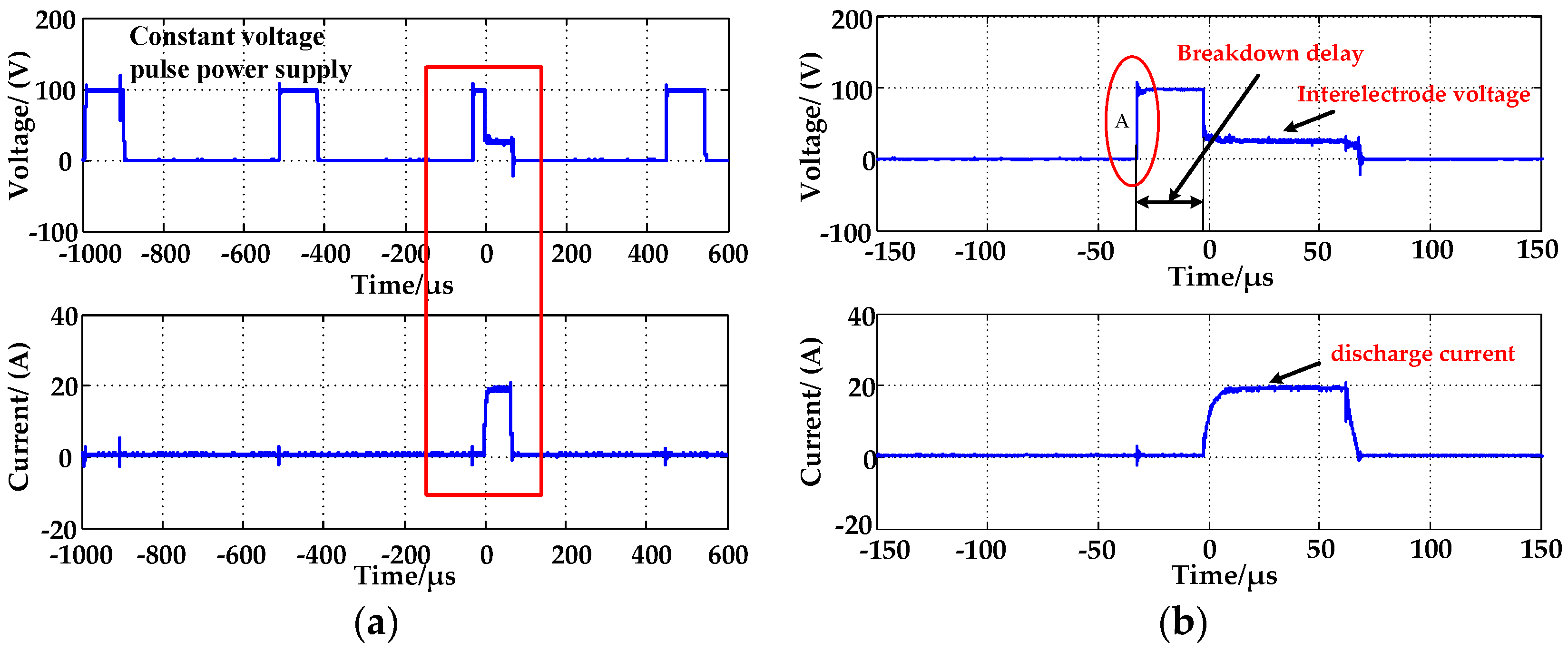
For the EDM discharge test, the interelectrode voltage and current waveforms are shown in Figure 3. Under the action of the constant voltage pulse power supply, the discharge current can be formed after the interelectrode dielectric is broken down. When the interelectrode dielectric is not broken down, there is no discharge current in the discharge circuit, as shown in Figure 3a. Enlarge the red rectangle region in Figure 3a to get Figure 3b.
2.2. EDM Interelectrode Gap Modeling
Based on the EDM interelectrode structure feature (the electrode surface is parallel to the workpiece surface) combined with the interelectrode voltage signal, the EDM breakdown delay stage (regions A) can be used as the plate capacitor. Therefore, the interelectrode dynamic voltage (the voltage of the plate capacitor Cg) can be expressed as
where U is the pulse supply voltage and is the time constant of the first-order RC loop, which can be expressed as
where Rt is the total resistance of the circuit before discharge and Cg is the capacitance value of the interelectrode plate capacitance before discharge. According to Figure 2, Rt and Cg can be expressed as
Combining Equations (2) and (4), the interelectrode gap d can be expressed as
where ε is the dielectric constant of the insulating working fluid medium before discharge, S is the effective area of the plate capacitance, and k is the electrostatic force constant. Then,
Combining Equations (5) and (6), the expression for the EDM interelectrode gap d can be obtained:
2.3. Determination of β
Figure 4 is obtained by amplifying the voltage signal of region A in Figure 3. According to the characteristics of the voltage signal across the flat-plate capacitor of the RC circuit, when t = , uc(t) = 0.63 U. When the interelectrode gap d changes, the capacitance Cg of the panel capacitor also changes accordingly, resulting in a change of the time constant . Therefore, in the single-pulse discharge test of EDM, it was only necessary to detect the time t during which the voltage across the plate capacitor rose from 0 to 0.63 U in order to determine the constant .
The rod copper electrode was used in the experiment and the electrode diameter was 10 mm. The workpiece material was p-type single-crystal Si, and the parameters are shown in Table 1. The no-load voltage of the pulse power supply was U = 100 V, and the pulse width and pulse interval of the power supply were 100 μs and 400 μs, respectively. Considering the randomness in EDM, each set of tests was conducted three times, and the test data is shown in Table 2. is the average value of β in three trials.
A least-squares fit was performed on the experimental data in Table 2, and the fitting curve is shown in Figure 5. The R2 of the least-squares fit between and the interelectrode gap d was 0.9977. The closer the value is to 1, the higher the correlation between the fitted value and the experimental value. The correction coefficient (Adj R2) was 0.9971, which means that 0.29% of the test data cannot be explained by this fitting expression. The root-mean-square error (RMSE) was 0.4453, which indicates a high degree of fitting. The least-squares fitting expression between and the interelectrode gap d is as follows:
According to Equations (7) and (8), the model expression of the EDM interelectrode gap d can be obtained as
2.4. Analysis of β
It can be learned from Equation (6) that β should be a constant, but the dielectric properties of the insulating working fluid in which electrodes were immersed changed during the discharge process, resulting in β not being constant in the test. Because the insulating working fluid media had good dielectric properties under the initial test conditions, in the single-pulse discharge test, the metal particles, carbon particles, and colloidal particles generated during the discharge process were diffused into the insulating medium. Since these materials have certain electrical conductivity that is equivalent to a piece of iron plate inserted into the insulating medium of the plate capacitor, and this effect is equivalent to the interelectrode gap decrease of the plate capacitor, the capacitance value Cg of the plate capacitor therefore increases. From Formula (2), we can see that the time constant will increase, and so the product β of the interelectrode gap d and the time constant will increase. However, with the auxiliary effect of interelectrode flushing, the metal particles, carbon particles, and colloidal particles in the interelectrode insulating medium will reach saturation at a certain concentration, and as the discharge continues, β will not change substantially.
2.5. Verification of EDM Interelectrode Gap Model
The established model was verified by using an EDM single-pulse discharge test. The voltage of the pulsed power supply was 100 V, the pulse width was 100 μs, and the interval pulse was 400 μs. All of these parameters were kept constant. The interelectrode gap ranged from 10 to 80 μm, increasing by 10 μm each time. The time constant was introduced into the EDM interelectrode gap model by Equation (9), from which the interelectrode gap d can be calculated. Each group was conducted 30 times. According to error theory, the 3-test method was used to analyze the test data. is the standard deviation, which is expressed below as
where, when n ≥ 25 for a certain observation data xi, its residual vi is satisfied as below:
The observation data xi is the gross error, where is the mean of observation data xi:
Table 3 shows the actual gap value as well as the minimum, maximum, and average values of the model-calculated gap of the 30 sets of tests. The values of the maximum absolute error δmax under each gap are also given.
Using a rectangular coordinate system, the horizontal axis is the gap d calculated by the model and the vertical axis is the actual gap. The minimum, maximum, and average values of the gap calculated by the model are plotted in Figure 6. It can be seen from the figure that the minimum, maximum, and average gap values calculated by the model are within ±3, where is the minimum value 0.9165 in Table 3. Therefore, there is no gross error in the gap d calculated by the model. When the actual gap is 80 μm, the maximum absolute error δmax between the calculated gap and the actual gap is only 2.31 μm, which indicates that the established interelectrode gap model is correct and reliable. As the actual gap increases, the absolute error between the calculated gap and the actual gap of the model also increases. This is because the fitting error between β and the interelectrode gap d increases as the interelectrode gap increases. It can be seen in Figure 5 that the degree of dispersion of several fitting curves reaches the maximum at 80 μm.
3. Order Identification Based on EDM System
In the actual process, due to the real-time erosion of the workpiece and electrode, the interelectrode gap d changes dynamically. By detecting the time constant in real time, the interelectrode gap d can be calculated by using the interelectrode gap model established by the previous section. In this study, the motion position of the electrode was used as the control input and the interelectrode gap d as the output. By continuously adjusting the electrode position, the interelectrode gap d can be precisely controlled. Combined with the characteristics of the EDM system, system identification theory [26] was used to establish a single-input, single-output (SISO) model. On the basis of input and output data, the order of the model was identified.
The determinant ratio method directly identified the order of the model by adopting the input and output data. First of all, the data matrix was constructed. Then, the determinant ratio of the matrix was used to construct the expression . When is a positive integer starting from one, if has a significant increase relative to , then is considered to be closer to the true order, i.e., the order of the model can be taken.
The model of single-input, single-output process is described as:
where is the input variable of the process. In the identification process, represents the moving position of the electrode. is the output variable of the process and the interelectrode gap d. is the uncorrelated random noise with the mean value of zero and the variance . and are the delay operator polynomials:
The estimated value of the model order is , using the existing input and output data to construct the following matrix :
where L is the data length.
In order to improve the accuracy of order discrimination as much as possible and to reduce the influence of error factors, the following determinant ratio was constructed to determine the order of the model:
where
When is a positive integer starting from one and if is significantly increased compared to , then can be considered as close to the real order of the model, i.e., the order of the model can be taken as .
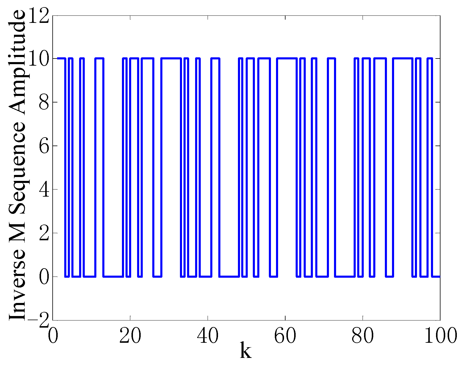
The M sequence is a binary pseudorandom code sequence the autocorrelation function of which is close to the pulse function. However, the M sequences contain DC components, which can cause “net disturbances” to the identified objects. The spectral density of the inverted M sequence is similar to that of the M sequence, which is twice as large as that of the M sequence and has no direct current component. Therefore, in this study, the order of the EDM system was identified using the inverse M sequence that can fully stimulate various modes of the system. Combined with the characteristics of the EDM system and in view of the continuous erosion of the workpiece and the electrode in the actual processing, the amplitude of the reverse M sequence was set to 0 and 10 μm after repeated trials. The input signal of the inverse M sequence in the identification process is shown in Figure 7. The data length L of the inverse M sequence was 100. Zero means that the electrode remains in the original place and 10 μm means that the electrode moves 10 μm toward the workpiece. The experiment was repeated three times, and can be calculated by using the determinant ratio method. The results are shown in Figure 8. It can be seen from the figure that when changes from 1 to 2, has a significant increase compared with , so the order of the EDM system model is .
4. Parameter Estimation and Controller Design Based on EDM System
4.1. Parameter Estimation
After the model order of the EDM system was determined, the parameters of the model needed to be estimated. The least-squares recursive algorithm is used to estimate the parameters in actual projects. With the increase of data collection, in order to prevent “data saturation”, this paper used the forgetting factor recursive least-squares method to estimate the parameters of the system. Since EDM is a two-order system, for the SISO system model described in Equation (13), the least-squares expression is
where a1, a2, b0, and b1 are model parameters, is the moving position of the electrode, and is the interelectrode gap d.
Equation (18) can be written as
where
The parameter estimation formula for the forgetting factor recursive least-squares method can be derived by using the performance indicators shown in Equation (21):
where λ (0 < λ ≤ 1) is the forgetting factor and P is the covariance matrix.
4.2. Controller Design
Adaptive control can make the system work automatically in the optimal or near-optimal operating state and obtain high-quality control performance under the condition that the model knowledge or environmental knowledge of the controlled object is incomplete or little known. The minimum-variance self-tuning controller adapts a recursive least-squares method to estimate the system parameters and uses the variance of the output error of the system as a performance index function by minimizing the performance index to calculate the control law. Finally, according to the calculated control law, the parameters are adjusted to realize the process control. Consider the following system:
where and represent the moving position of the electrode and interelectrode gap, respectively. C(z–1) is a Hurwitz polynomial, is white noise with variance , is the number of pure delays, and
The interelectrode gap at iteration k + d is based on the electrode position and gap measurement at iteration k and the previous iteration. This predicted gap at iteration k + d is denoted as , and the prediction error is
The interelectrode gap prediction error variance is
The minimum d-step optimal prediction output with in the above performance index Formula (25) needs to satisfy the equation below:
where
and
Equation (26) is called the optimal output prediction equation, and Equation (27) is called the Diophantine equation.
Therefore, the minimum-variance control law is
From Equation (29), the control law is
where yr are the reference gaps, y are the measurement gaps, and the control variable at the current moment is calculated by the above formula and acts on the system, which completes the control of current time. Therefore, the minimum-variance self-correcting control is realized by such reciprocal execution.
5. Test Verification
The EDM equipment shown in Figure 1 was modified to meet the control requirements for the interelectrode gap in the machining. The improved EDM control system is shown in Figure 9. The no-load voltage of the pulse power supply was 100 V, the pulse width was 100 μs, the pulse interval was 400 μs, and the workpiece was p-type monocrystalline silicon. Since the no-load voltage between the electrodes was 100 V, the signal adjusting module was developed for linear transformations of the interelectrode output voltage. The output voltage range of the signal adjusting module was 0–10 V. Since the interelectrode gap model d was calculated based on the time constant when the voltage rose to 0.63 U, the sampling frequency of the data acquisition card was relatively high. The high-speed data acquisition card PXle-5172 from NI (National instruments, Austin, TX, USA) was used for high-speed acquisition of the voltage signal and data acquisition. The bandwidth of the data acquisition card was 100 MHz, the sampling frequency was 250 MS/s, and the input voltage range was −40 to 40 V. The PXle-7342 motion controller of NI (National instruments, Austin, TX, USA) was used to control the motor movement, and the pulse output rate of the motion controller was up to 4 MHz. The motor was a Yaskawa SGM7J-04AFC6S servo motor (National instruments, Austin, TX, USA) used in the position control mode. Through the calibration test, the positioning accuracy of the EDM system could reach 1 μm. The position of the electrode was adjusted every 0.1 s during the test.
5.1. Stability Tracking Verification
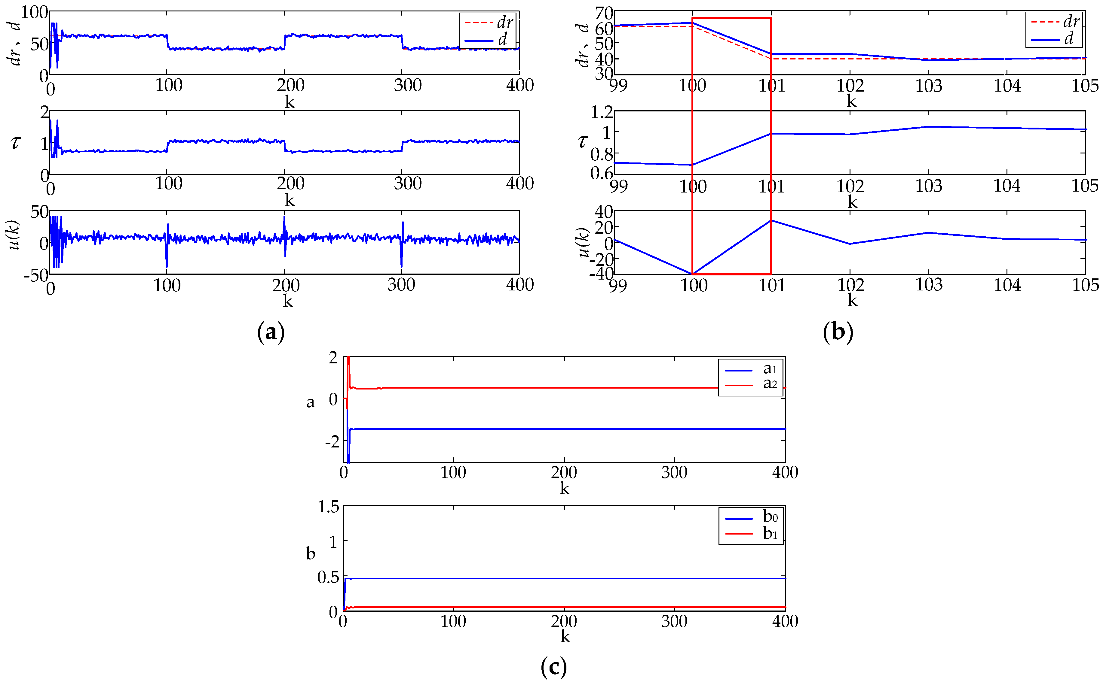
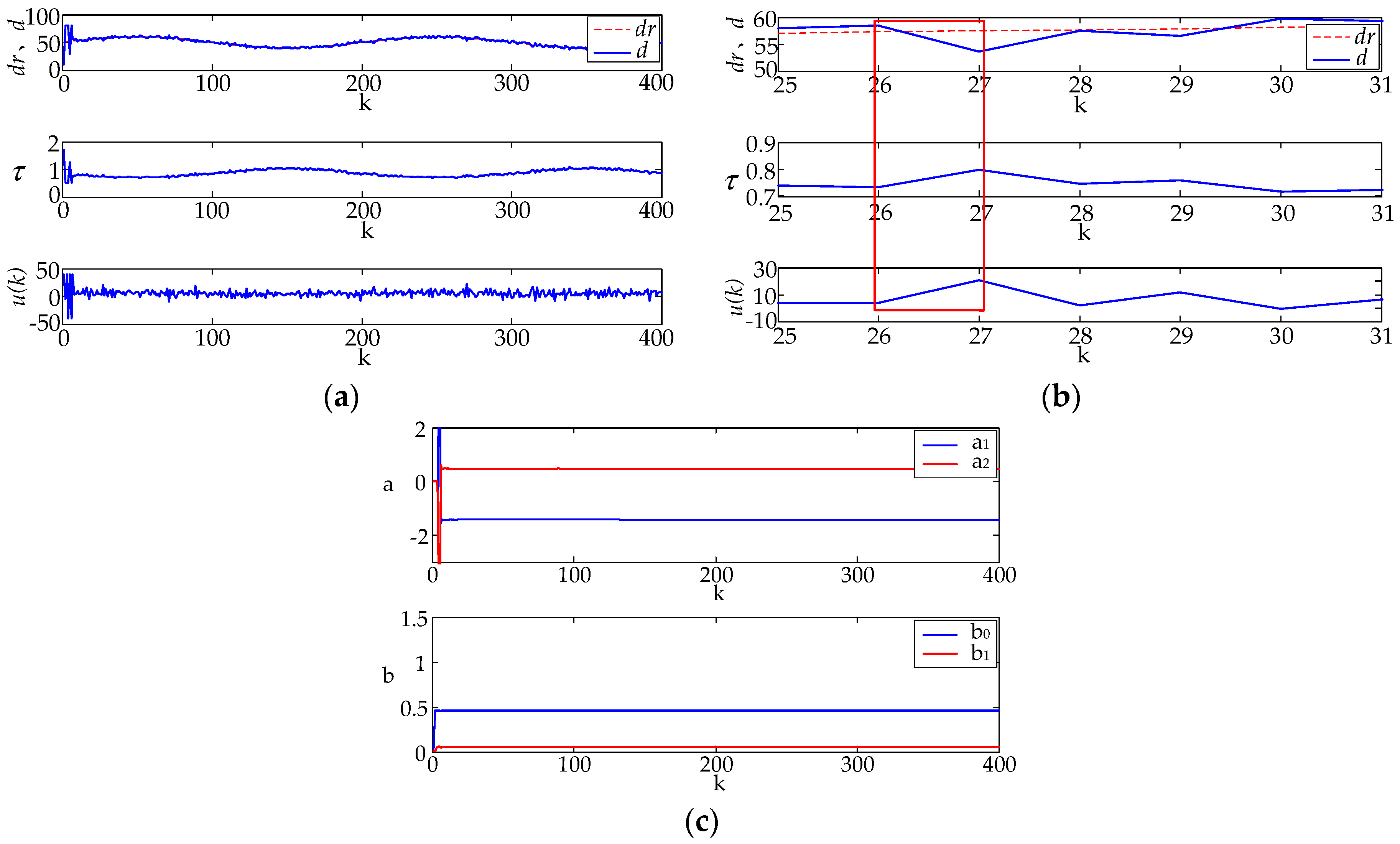
In order to verify the stability of the minimum-variance self-tuning controller, the p-type single-crystal silicon processing experiment was carried out by using the minimum-variance self-tuning control on the improved EDM control system. During the test, the motor was in position control mode and the electrode movement speed was 2 cm/s. In actual processing, in order to prevent short-circuit phenomena, after repeated tests, the absolute distance of the electrode positive feed does not exceed 40 μm. Since the detection range of the interelectrode gap model established in the first section was 10–80 μm, the output range of the control system was limited to 10–80 μm. The tracking input signal was separately a straight line, a square wave, a sine wave, and the output was a time constant . Equation (9) was used to further convert into the interelectrode gap d. Figure 10, Figure 11 and Figure 12 show the tracking effect of the input signal and parameter identification effects.
From the tracking effect in the actual machining process, it can be seen that the system had a certain adjustment time of 2 s in the initial stage of processing. Then, the interelectrode distance d could stably track the different interelectrode gap expected value dr. The right side of the tracking diagram is a local enlarged view. It can be seen from the red area in the local enlarged view that if the interelectrode gap d increases and the electrode is retracted, while d decreases, the electrode is fed to the workpiece. Therefore, the variation of the interelectrode gap is consistent with the actual advance and retreat of the electrode. It can be seen from the figure that the estimated values of parameters a and b are stable. The verification results show that the controller performs well and the parameters identified on-line are stable.
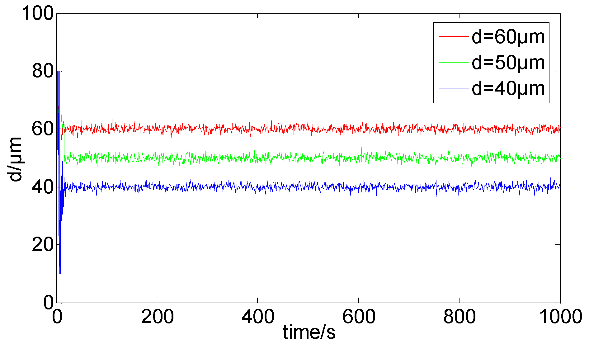
5.2. Comparison and Verification of Process Targets under Different Gap Conditions
EDM uses the high-temperature plasma generated by the discharge to remove the workpiece. The plasma energy is mainly determined by the interelectrode voltage and the loop current, while the material removal rate and the surface roughness in EDM are influenced by the interelectrode voltage and loop current. The literature [27] has studied the effect of the interelectrode gap on the interelectrode voltage and loop current. Therefore, it is of great significance to study the effect of the interelectrode gap on the material removal rate and surface roughness of EDM. A single-crystal silicon processing experiment was conducted by using the minimum-variance self-tuning control, and the interelectrode gap desired value was 60, 50, and 40 μm. The test processing time at the three desired gaps was 100 s. The tracking effect of the three different desired gaps is shown in Figure 13.
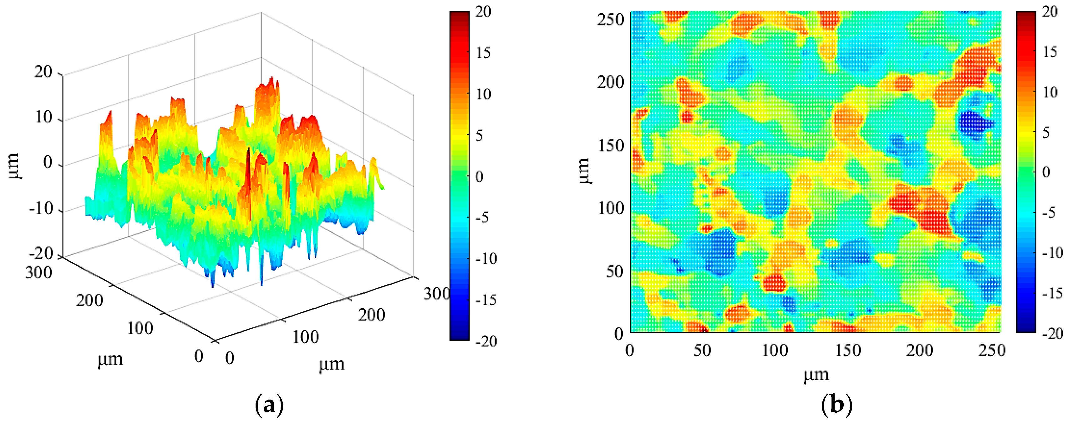
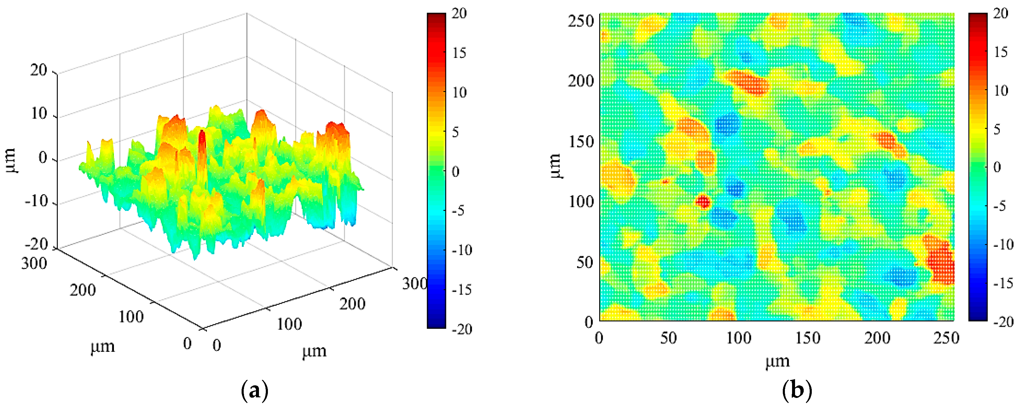
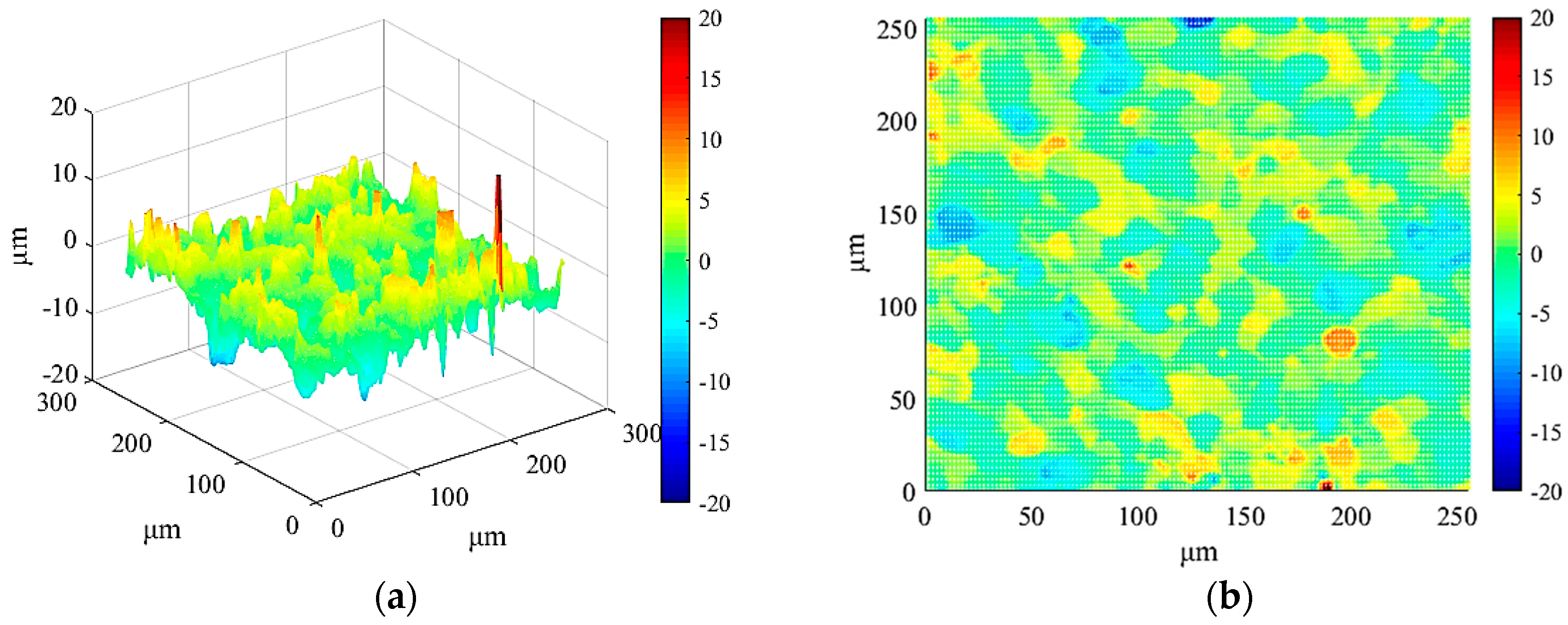
After the test was completed, the mass of single-crystal silicon before and after machining was measured by the JD500-3 precision electronic balance (Shenyang Longteng Electronics Co., Ltd, Shenyang, Liaoning, China) to calculate the material removal rate. The balance’s maximum measurement mass is 500 g, with an accuracy of 0.001 g. The surface morphology and roughness of the processed single-crystal silicon was measured by the Leica DCM 3D white light interferometer (Leica, Solms, Hessen, Germany). The three-dimensional surface and two-dimensional shape of the workpiece surface are shown in Figure 14, Figure 15 and Figure 16. The measurement results of material removal rate and surface roughness are shown in Table 4.
In the EDM system, the plasma channel diameter and pit size formed by a single-pulse discharge are determined by the current and the effective discharge time [28,29], and the higher the current and longer the effective discharge time, the larger the plasma channel diameter and the crater. In continuous pulse machining, the higher the current and the longer the effective discharge time, the greater the material removal rate and surface roughness. The quantitative relationship between the plasma channel diameter and the interelectrode gap is given in Reference [27], and the larger the interelectrode gap, the smaller the loop current. Therefore, when the interelectrode gap increases, the loop current decreases, which leads to a reduction of the material removal rate and surface roughness. From Table 4, it can be seen that the material removal rate and surface roughness decrease with the increase of the interelectrode gap. The above analysis fully proves the rationality of the test results.
6. Conclusions
(1) Based on the EDM interelectrode structure characteristics, combined with the characteristics of the interelectrode voltage signal, a flat-plate capacitance model was introduced to quantitatively describe the mathematical relationship of the interelectrode gap d and the plate capacitor charging time constant . The reason for the increase of the proportional coefficient β of d and was analyzed and the model was verified by the 3-test method. The results show that the established EDM interelectrode gap model can correctly reflect the true value of the interelectrode gap. When the actual gap is 80 μm, the absolute error maximum value δmax of the calculated gap and the actual gap is only 2.31 μm, The EDM interelectrode gap model established in this study is universal. When the model is applied to metal or alloy materials with good conductivity, only the equivalent resistance RW of the single-crystal silicon needs to be removed from Equation (3). β can be redetermined by a single-pulse discharge test, and the EDM interelectrode gap model suitable for common metals and alloy materials can be further deduced.
(2) Using the system identification method to obtain the transfer function of the electrode position and the interelectrode gap, the order and parameters of the model were determined by the determinant ratio method and the forgetting factor recursive least-squares algorithm. A minimum-variance self-tuning controller was designed to realize the adaptive control of the electrode position. The interelectrode gap can be steadily tracked by adjusting the electrode position in real time, which provides a theoretical basis and practical reference for precise control of the interelectrode gap.
(3) The experimental verification results show that the minimum-variance self-tuning controller can effectively track various reference trajectories (straight lines, square waves, etc.). The minimum-variance self-correcting control was adopted to avoid the short-circuit phenomenon caused by the excessive feed rate of the electrodes. The smaller the interelectrode gap, the larger the discharge current, and the higher the machining efficiency, but the surface roughness will also increase.
Author Contributions
Conceptualization, B.X. and S.-J.L.; Methodology, B.X.; Software, X.-C.Y.; Validation, B.X., S.-J.L. and X.L.; Formal Analysis, B.X.; Investigation, B.X.; Resources, S.-J.L.; Data Curation, X.L.; Writing–Original Draft Preparation, B.X.; Writing–Review & Editing, B.X.; Project Administration, S.-J.L.; Funding Acquisition, S.-J.L.
Funding
The work is supported by the National Natural Science Foundation of China (No. 51575442) and the Shaanxi Provincial Natural Science Foundation (No. 2016JZ011).
Acknowledgments
Thank the National Natural Science Foundation of China and the Shaanxi Provincial Natural Science Foundation. Thanks to Shujuan Li for guiding the article. Thanks to other authors for their help with the article.
Conflicts of Interest
The authors declare no conflict of interest.
References
- Egashira, K.; Mizutani, K. Micro-drilling of monocrystalline silicon using a cutting tool. Precis. Eng. 2002, 26, 263–268. [Google Scholar] [CrossRef]
- Fang, F.Z.; Wu, H.; Liu, Y.C. Modelling and experimental investigation on nanometric cutting of monocrystalline silicon. Int. J. Mach. Tools Manuf. 2005, 45, 1681–1686. [Google Scholar] [CrossRef]
- Swiercz, R.; Oniszczuk-Swiercz, D. Experimental investigation of surface layer properties of high thermal conductivity tool steel after electrical discharge machining. Metals 2017, 7, 550. [Google Scholar] [CrossRef]
- Furutani, K.; Hiraoka, D. Condition Monitoring in concurrent micro-hole electrical discharge machining with electrode feeding devices employing AZARASHI (Seal) mechanism. Procedia CIRP 2014, 14, 424–429. [Google Scholar] [CrossRef]
- Abidi, M.H.; Al-Ahmari, A.M.; Siddiquee, A.N.; Main, S.H.; Mohammed, M.K.; Rasheed, S.M. An Investigation of the Micro-Electrical Discharge Machining of Nickel-Titanium Shape Memory Alloy Using Grey Relations Coupled with Principal Component Analysis. Metals 2017, 7, 486. [Google Scholar] [CrossRef]
- Chen, H.R.; Liu, Z.D.; Huang, S.J.; Pan, H.J.; Qiu, M.B. Study of the mechanism of multi-channel discharge in semiconductor processing by WEDM. Mater. Sci. Semicond. Process. 2015, 32, 125–130. [Google Scholar] [CrossRef]
- Puertas, I.; Luis, C.J.; Villa, G. Spacing roughness parameters study on the EDM of silicon carbide. J. Mater. Process. Technol. 2005, 164, 1590–1596. [Google Scholar] [CrossRef]
- Luis, C.J.; Puertas, I.; Villa, G. Material removal rate and electrode wear study on the EDM of silicon carbide. J. Mater. Process. Technol. 2005, 164, 889–896. [Google Scholar] [CrossRef]
- Ji, R.; Liu, Y.; Zhang, Y.; Cai, B.; Li, X. High-speed end electric discharge milling of silicon carbide ceramics. Mater. Manuf. Processes 2011, 26, 1050–1058. [Google Scholar] [CrossRef]
- Salcedo, A.T.; Arbizu, I.P.; Pérez, C.J.L. Analytical modelling of energy density and optimization of the EDM machining parameters of Inconel 600. Metals 2017, 7, 166. [Google Scholar] [CrossRef]
- Kunieda, M.; Lauwers, B.; Rajurkar, K.P.; Schumacher, B.M. Advancing EDM through fundamental insight into the process. CIRP Ann. 2005, 54, 64–87. [Google Scholar] [CrossRef]
- Mahardika, M.; Mitsui, K. A new method for monitoring micro-electric discharge machining processes. Int. J. Mach. Tools Manuf. 2008, 48, 446–458. [Google Scholar] [CrossRef]
- Mahardika, M.; Tsujimoto, T.; Mitsui, K. A new approach on the determination of ease of machining by EDM processes. Int. J. Mach. Tools Manuf. 2008, 48, 746–760. [Google Scholar] [CrossRef]
- Rajurkar, K.P.; Wang, W.M.; Lindsay, R.P. A new model reference adaptive control of EDM. CIRP Ann. 1989, 38, 183–186. [Google Scholar] [CrossRef]
- Behrens, A.W.; Ginzel, J.; Bruhns, F.L. Threshold technology and its application for gap status detection. J. Mater. Process. Technol. 2004, 149, 310–315. [Google Scholar] [CrossRef]
- Han, F.; Wachi, S.; Kunieda, M. Improvement of machining characteristics of micro-EDM using transistor type isopulse generator and servo feed control. Precis. Eng. 2004, 28, 378–385. [Google Scholar] [CrossRef]
- Tarng, Y.S.; Tseng, C.M.; Chung, L.K. A fuzzy pulse discriminating system for electrical discharge machining. Int. J. Mach. Tools Manuf. 1997, 37, 511–522. [Google Scholar] [CrossRef]
- Kao, J.Y.; Tarng, Y.S. A neutral-network approach for the on-line monitoring of the electrical discharge machining process. J. Mater. Process. Technol. 1997, 69, 112–119. [Google Scholar] [CrossRef]
- Rajurkar, K.P.; Wang, W.M. Improvement of EDM performance with advanced monitoring and control systems. J. Manuf. Sci. Eng. 1997, 119, 770–775. [Google Scholar] [CrossRef]
- Rajurkar, K.P.; Wang, W.M.; Lindsay, R.P. Real-time stochastic model and control of EDM. CIRP Ann. 1990, 39, 187–190. [Google Scholar] [CrossRef]
- Weck, M.; Dehmer, J.M. Analysis and adaptive control of EDM sinking process using the ignition delay time and fall time as parameter. CIRP Ann. 1992, 41, 243–246. [Google Scholar] [CrossRef]
- Kao, C.C.; Shih, A.J. Design and tuning of a fuzzy logic controller for micro-hole electrical discharge machining. J. Manuf. Processes 2008, 10, 61–73. [Google Scholar] [CrossRef]
- Kao, C.C.; Shih, A.J.; Miller, S.F. Fuzzy logic control of microhole electrical discharge machining. J. Manuf. Sci. Eng. 2008, 130, 1786–1787. [Google Scholar] [CrossRef]
- Kaneko, T.; Onodera, T. Improvement in machining performance of die-sinking EDM by using self-adjusting fuzzy control. J. Mater. Process. Technol. 2004, 149, 204–211. [Google Scholar] [CrossRef]
- Shabgard, M.R.; Badamchizadeh, M.A.; Ranjbary, G.; Amini, K. Fuzzy approach to select machining parameters in electrical discharge machining (EDM) and ultrasonic-assisted EDM processes. J. Manuf. Syst. 2013, 32, 32–39. [Google Scholar] [CrossRef]
- Li, S.; Du, S.; Tang, A.; Landers, G.L.; Zhang, Y. Force modeling and control of SiC monocrystal wafer processing. J. Manuf. Sci. Eng. 2015, 137, 061003. [Google Scholar] [CrossRef]
- Kojima, A.; Natsu, W.; Kunieda, M. Spectroscopic measurement of arc plasma diameter in EDM. CIRP Ann. 2008, 57, 203–207. [Google Scholar] [CrossRef]
- Li, M.H. Electric discharge machining surface characteristics. In EDM Theoretical Basis; National Defense Industry Press: Beijing, China, 1989. [Google Scholar]
- Ikai, T.; Hashigushi, K. Heat input for crater formation in EDM. In Proceedings of the International Symposium for Electro-Machining (ISEM XI), EPFL, Lausanne, Switzerland, 17–21 April 1995; pp. 163–170. [Google Scholar]
Figure 1.
Electric discharge machining (EDM) test equipment.

Figure 2.
EDM discharge circuit model.

Figure 3.
EDM discharge waveform: (a) The overall waveform; (b) The locally amplified waveform.

Figure 4.
Voltage rising edge waveform.

Figure 5.
Relation curve between β and the interelectrode gap.

Figure 6.
Distribution relationship between actual gap and model-calculated gap.

Figure 7.
Input inverse M sequence.

Figure 8.
Order identification result.

Figure 9.
EDM control system schematic.

Figure 10.
Straight line tracking: (a) The original image; (b) partial enlargement; (c) parameter identification result.
Figure 10.
Straight line tracking: (a) The original image; (b) partial enlargement; (c) parameter identification result.

Figure 11.
Square wave tracking: (a) The original image; (b) partial enlargement; (c) parameter identification result.
Figure 11.
Square wave tracking: (a) The original image; (b) partial enlargement; (c) parameter identification result.

Figure 12.
Sine wave tracking: (a) The original image; (b) partial enlargement; (c) parameter identification result.
Figure 12.
Sine wave tracking: (a) The original image; (b) partial enlargement; (c) parameter identification result.

Figure 13.
Three different desired tracking effects.

Figure 14.
Three-dimensional surface topography and two-dimensional surface topography (d = 40 μm). (a) Three-dimensional surface topography; (b) two-dimensional surface topography.
Figure 14.
Three-dimensional surface topography and two-dimensional surface topography (d = 40 μm). (a) Three-dimensional surface topography; (b) two-dimensional surface topography.

Figure 15.
Three-dimensional surface topography and two-dimensional surface topography (d = 50 μm). (a) Three-dimensional surface topography; (b) two-dimensional surface topography.
Figure 15.
Three-dimensional surface topography and two-dimensional surface topography (d = 50 μm). (a) Three-dimensional surface topography; (b) two-dimensional surface topography.

Figure 16.
Three-dimensional surface topography and two-dimensional surface topography (d = 60 μm). (a) Three-dimensional surface topography; (b) two-dimensional surface topography.
Figure 16.
Three-dimensional surface topography and two-dimensional surface topography (d = 60 μm). (a) Three-dimensional surface topography; (b) two-dimensional surface topography.


Table 1.
Parameters of p-type monocrystalline silicon.
| P-Type Monocrystalline Silicon | Diameter (1 in) | Growth Mode | Straight Pull Single Crystal (CZ) |
|---|---|---|---|
| Thickness of Si wafer | 5 mm | Doping type | Boron doping |
| Crystal orientation | <111> | Resistivity | 0.1 Ω cm |
| Melting point | 1410 °C | Boiling point | 2355 °C |
| Density | 2.33 g/cm³ |
Table 2.
Test data.
| Actual Gap (μm) | β1 | β2 | β3 | ||||
|---|---|---|---|---|---|---|---|
| 10 | 1.62 | 16.2 | 1.63 | 16.3 | 1.64 | 16.4 | 16.3 |
| 15 | 1.58 | 23.7 | 1.57 | 23.55 | 1.57 | 23.55 | 23.6 |
| 20 | 1.51 | 30.2 | 1.52 | 30.4 | 1.49 | 29.8 | 30.13 |
| 25 | 1.37 | 34.3 | 1.39 | 34.75 | 1.36 | 34 | 34.35 |
| 30 | 1.23 | 36.9 | 1.22 | 36.6 | 1.24 | 37.2 | 36.9 |
| 35 | 1.1 | 38.5 | 1.13 | 39.55 | 1.12 | 39.2 | 39.08 |
| 40 | 1.02 | 40.8 | 1.05 | 42 | 1.04 | 41.6 | 41.47 |
| 45 | 0.95 | 42.75 | 0.93 | 41.85 | 0.94 | 42.3 | 42.3 |
| 50 | 0.86 | 43 | 0.88 | 44 | 0.87 | 43.5 | 43.5 |
| 55 | 0.78 | 42.6 | 0.77 | 42.35 | 0.77 | 42.35 | 42.43 |
| 60 | 0.71 | 42.75 | 0.72 | 43.2 | 0.70 | 42.0 | 42.65 |
| 65 | 0.66 | 42.9 | 0.65 | 42.25 | 0.65 | 42.25 | 42.47 |
| 70 | 0.61 | 42.7 | 0.62 | 43.4 | 0.60 | 42.0 | 42.7 |
| 75 | 0.57 | 42.75 | 0.58 | 43.5 | 0.57 | 42.75 | 43 |
| 80 | 0.54 | 42.4 | 0.55 | 44 | 0.54 | 43.2 | 43.2 |
Table 3.
Actual gap and model-calculated gap.
| Actual Gap (μm) | Model-Calculated Gap (μm) | Model-Calculated Mean Gap | δmax | |
|---|---|---|---|---|
| 10 | 9.1562 | 10.2138 | 1.2168 | 1.10 |
| 11.1022 | ||||
| 20 | 18.5918 | 19.8764 | 1.1365 | 1.41 |
| 20.7725 | ||||
| 30 | 29.4844 | 30.3362 | 1.0687 | 1.61 |
| 31.6051 | ||||
| 40 | 39.0474 | 40.0568 | 0.9165 | 1.14 |
| 41.1400 | ||||
| 50 | 48.8590 | 50.2152 | 0.9862 | 1.57 |
| 51.5708 | ||||
| 60 | 58.3669 | 59.8568 | 0.9676 | 1.73 |
| 61.7297 | ||||
| 70 | 68.1800 | 69.7634 | 1.2043 | 1.82 |
| 71.1806 | ||||
| 80 | 78.7784 | 80.2652 | 1.1862 | 2.31 |
| 82.3050 |
Table 4.
Material removal rate and surface roughness data.
| Interelectrode Gap (μm) | Material Removal Rate (mg/min) | Surface Roughness (μm) |
|---|---|---|
| 40 | 51 | 7.35 |
| 50 | 46 | 5.66 |
| 60 | 39 | 4.58 |
© 2018 by the authors. Licensee MDPI, Basel, Switzerland. This article is an open access article distributed under the terms and conditions of the Creative Commons Attribution (CC BY) license (http://creativecommons.org/licenses/by/4.0/).
Share and Cite
MDPI and ACS Style
Xin, B.; Li, S.; Yin, X.; Lu, X. Dynamic Observer Modeling and Minimum-Variance Self-Tuning Control of EDM Interelectrode Gap. Appl. Sci. 2018, 8, 1443. https://doi.org/10.3390/app8091443
AMA Style
Xin B, Li S, Yin X, Lu X. Dynamic Observer Modeling and Minimum-Variance Self-Tuning Control of EDM Interelectrode Gap. Applied Sciences. 2018; 8(9):1443. https://doi.org/10.3390/app8091443
Chicago/Turabian StyleXin, Bin, Shujuan Li, Xincheng Yin, and Xiong Lu. 2018. "Dynamic Observer Modeling and Minimum-Variance Self-Tuning Control of EDM Interelectrode Gap" Applied Sciences 8, no. 9: 1443. https://doi.org/10.3390/app8091443
Note that from the first issue of 2016, this journal uses article numbers instead of page numbers. See further details here.