1. Introduction
Light-emitting diode (LED) lighting has many advantages, such as high lighting efficiency, a compact size, and fast response. When compared with fluorescent lamps, LEDs are more environmentally friendly because they do not use mercury. As such, with these features, the usage of LED lighting has become an irresistible trend. Among the various advantages of LED, the most prominent still focuses on its high lighting efficiency, although not all questions about the interaction between humans and light emitted by the LEDs have been completely solved [
1,
2,
3]. Nowadays, in pursuit of things such as high lighting quality, special lighting atmospheres, and/or energy-saving capacities, many LED lights have incorporated a dimming function. However, because there are many people who do not require higher-quality lighting, LED lighting without the dimming function is still widely used, such as in household or street lighting. For such lights, the key factor of lighting equipment selection depends on the cost–performance ratio of the product [
4,
5,
6]. Thus, the development of a simple and low-cost LED driver is likely to greatly enhance the popularity of LED lighting.
In the highly-competitive lighting market, the lighting drive circuit, using a self-excited control mechanism, has been widely used in many low-price products—especially in the applications of electronic ballast [
7,
8,
9,
10]. The purpose of a self-excited circuit is to drive the power switches repeatedly by using the polarity changes of the voltage across windings of a magnetic component, meaning that it does not need to use an integrated circuit (IC), and the components used to build a direct-current (dc) voltage for the IC can be saved. In the conventional self-excited fluorescent lamp electronic ballast, the circuit topology possesses a half-bridge (inductor-capacitor-capacitor) (LCC) resonant circuit by introducing a saturable transformer connected in series with a resonant circuit to generate the self-excited driving voltage that can drive bipolar junction transistors (BJT) [
11,
12,
13]. Regarding driving a BJT, when it is used as a power switch, it requires a base current sufficiently high enough to drive the BJT to operate in the saturation region. However, driving a BJT into the saturation region will influence the charge carrier behavior in the (positive-negative) (PN) junction, thus further affecting the switching time thereof. In general, there are many such uncontrollable factors, including things like saturation point of an iron core, storage time carriers, ambient temperature, and humidity—and all of them hinder the precise control of the resonant frequency and voltage gain of the resonant circuit.
On the other hand, active power-factor correctors (PFCs) are widely applied to the lighting circuit due to the increasingly strict regulations on power quality. Although the power factor can be effectively improved by adding a PFC circuit to the original lighting circuit, the number of circuit components then need to be increased, resulting in an uneconomical solution. Thus, aiming to find a cost-effective solution, researchers proposed some single-stage lighting circuits with self-excited control schemes by integrating a PFC and dc-to-dc resonant circuit [
14,
15,
16]. However, using BJT as power switches invokes further problems [
17], because among these single-stage circuits, two power BJTs could suffer from uneven current and lead to unequal conduction time between the two BJTs, thus making the simplification of single-stage PFC impossible.
In this paper, a novel single-stage LED driver with a self-excited mechanism through integration of a boost-type PFC and a half-bridge series resonant converter is proposed. No additional integrated circuit is required. The driving voltages of the self-excited mechanism are taken directly from the center-tapped transformer, which is cascaded by a full-wave diode rectifier to obtain the dc output voltage. As compared with the traditional self-excited mechanism, it does not need to use an easily saturable transformer—thus, the number of components can be reduced. Two metal-oxide-semiconductor field-effect transistors (MOSFETs) serve as the power switches. The MOSFET is a voltage-driven component. Unlike the BJT-based circuit topology, the core saturation and carrier storage time problems can be avoided, thus making the circuit design easier. Moreover, since MOSFETs are used in the single-stage PFC circuit, the incidence of unequal currents in power switches is far less, meaning the uneven conduction times between the switches can be ignored. Therefore, the developed self-excited method is quite suitable for single-stage PFC application. In addition, the switching frequency of the MOSFETs can be identical to the resonant frequency of the resonant converter. The resonant converter operates at the resistive mode, thus accomplishing both the zero-voltage switching (ZVS) and zero-current switching (ZCS) performance of power switches [
18,
19,
20,
21]. Consequently, the developed self-excited single-stage converter will possess the advantages of having both a high power factor and low switching losses, and is also suitable for LED drive application.
2. Proposed Circuit Topology and Operation Analysis
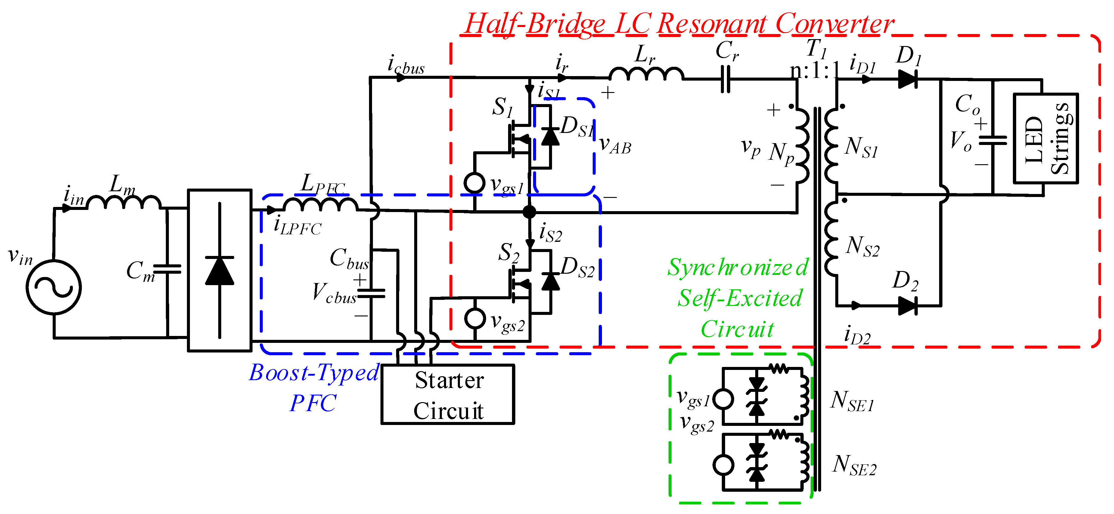
In our particular study, a half-bridge inductor-capacitor (LC) resonant converter, a boost-typed PFC, a starter circuit, and the developed self-excited circuit were integrated to constitute the novel single-stage structure, as shown in
Figure 1. A list of symbols is as follows.
S1, S2: power switches; DS1, DS2: intrinsic body diodes of the power switches, LPFC: inductance of the boost-typed PFC, T1: center-tapped transformer, Np: turns of the primary winding, NS1, NS2: turns of the secondary windings, NSE1, NSE2: turns of the self-excited windings, D1, D2: full-wave rectifier diodes, Lr: inductance of the resonant inductor, Cr: capacitance of the resonant capacitor, Lm: inductance of the low-pass filter, Cm: capacitance of the low-pass filter, Cbus: capacitance of the dc-bus capacitor, and Co: capacitance of the output capacitor.
vin: input line voltage, iin: input line current, iLPFC: PFC inductor current, Vcbus: dc-bus voltage, icbus: dc-bus current, Vo: output voltage, vgs1: gate-to-source voltage of S1, vgs2: gate-to-source voltage of S2, iS1: drain-to-source current of S1, iS2: drain-to source current of S2, ir: resonant current of the resonant circuit, vAB: input voltage of the resonant circuit, vp: voltage across the primary winding, fr: resonant frequency of the resonant circuit, fs: switching frequency of power switches, Mvr: voltage gain of the resonant circuit, Q: quality factor of the resonant circuit, s: switching angular frequency, r: resonant angular frequency, Rp: equivalent load resistance across the primary winding, RLED: equivalent resistance of the LED string, and D: duty ratio of the power switches.
MOSFETs
S1 and
S2 acted as power switches, and the antiparallel diodes
DS1 and
DS2 as their intrinsic body diodes, respectively. The center-tapped transformer
T1 and diodes
D1 and D
2 formed a full-wave rectifier. The turn ratio of the primary winding to the secondary windings was n: 1:1. In addition,
T1 had two more windings which were employed to provide power switches with self-excited driving voltages. Besides,
T1 could provide galvanic insulation with respect to the input line. The low-pass filter (
Lm and
Cm) was used to remove the high-frequency current of the inductor current, because in this way, the input line current would be sinusoidal with the same frequency as the input line voltage. For simplification of the circuit analysis, the capacitances of
Cbus and
Co were assumed to be large enough that the dc-bus voltage
Vcbus and the output voltage
V0 could be regarded as constant. As shown in
Figure 1, the power switch
S2 should carry both currents of the PFC converter and the resonant converter. The voltage across
S2 is equal to the dc-bus voltage when it is off. Hence,
S2 is the crucial component of the proposed circuit and its voltage and current ratings will determine the power range.
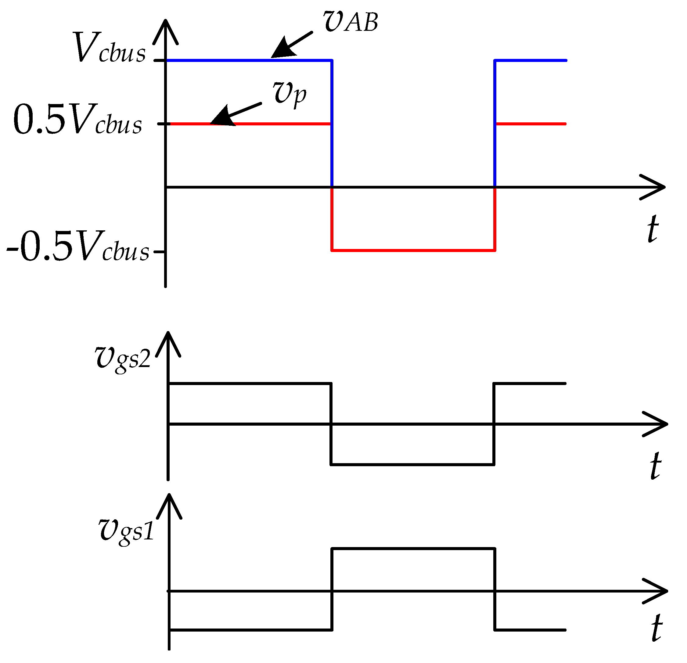
2.1. Self-Excited Driving Voltages
The center-tapped transformer has two additional windings—the turn ratio of the primary winding to the additional windings is m: 1:1. The self-excited driving voltages were obtained by stepping down the high-frequency square wave via the transformer. A pair of symmetrical square wave voltages (
vgs1,
vgs2) were generated by the self-excited windings, as depicted in
Figure 2. Their frequency
fs was in synchronism with the resonant frequency
fr which was created by the combination of resonant inductor
Lr and resonant capacitor
Cr, as can be expressed by Equations (1) and (2).
The voltage on the primary winding
vp of the transformer can be achieved by Equation (3),
where
Mvr is the voltage gain of the resonant circuit, and
D is the duty ratio of the lower-arm power switch
S2. The control voltages
vgs1 and
vgs2 may be approximated as square waves, equal to:
where the negative sign indicates the phase relationship between
vgs1 and
vgs2.
2.2. LC Resonant Converter
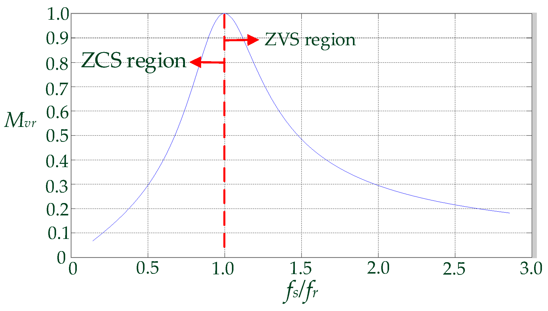
Since the self-excited driving voltages were directly obtained from the resonant circuit, the switching frequency of the power MOSFETs was, of course, synchronous with the resonant voltage waveform, thus making the switching frequency and the resonant frequency identical. The voltage gain
Mvr of the resonant circuit is defined as the ratio of the magnitude of
T1’s primary voltage to the magnitude of the input voltage, and can be expressed as:
where
Q is the quality factor of the resonant circuit,
ωs designates the switching angular frequency,
ωr is the resonant angular frequency, and
Rp represents the equivalent load resistance between the primary winding. At steady-state operation,
Rp can be expressed as [
22]:
where
RLED represents the equivalent impedance of the LED string.
Figure 3 depicts the relationship between voltage gain
Mvr and frequency ratio
fs/
fr based on Equations (5) and (6). It can be seen that the circuit exhibits capacitive characteristics when the switching frequency is smaller than the resonant frequency. The power switches will possess the feature of ZCS when
fs/
fr < 1. On the contrary, the circuit appears inductive when the switching frequency is greater than the resonant frequency. The power switches will possess ZVS when
fs/
fr > 1. As soon as the switching frequency and the resonant frequency are equal, the circuit possesses a resistive feature and the power switches can operate at both ZCS and ZVS.
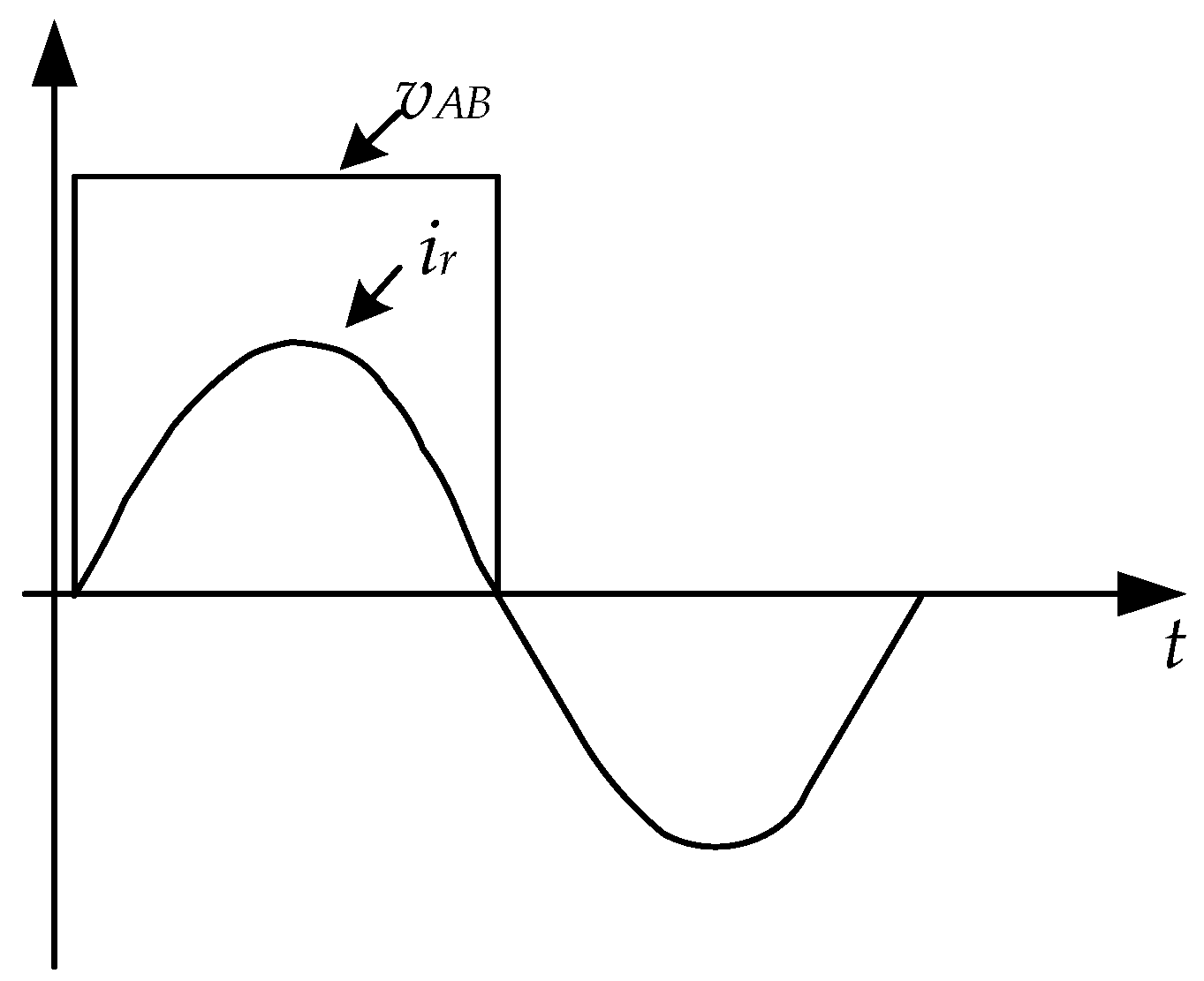
Figure 4 shows the ideally schematic waveforms of the input voltage of the resonant circuit
vAB and the resonant current
ir when
fs =
fr, i.e., that the voltage switches to zero the moment the resonant current reaches zero. This makes the power switch undergo no extra switching loss.
2.3. Boost-Typed Power-Factor Corrector
As shown in
Figure 1, the boost converter, which is composed of
LPFC,
S2,
DS1, and
Cbus, performs the function of PFC.
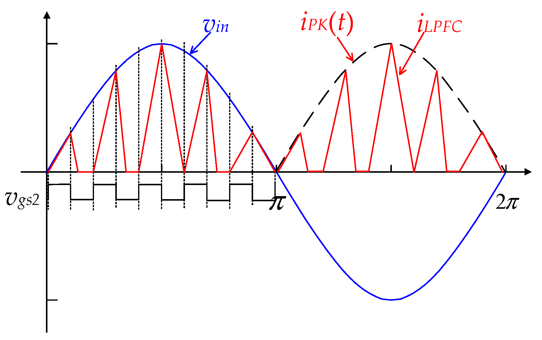
Figure 5 shows the PFC inductor current
iLPFC when the PFC circuit is designed to operate at discontinuous conduction mode (DCM). Since the rising slope of
iLPFC is proportional to the line voltage
vin, the envelope of
iLPFC would be sinusoidal. The alternating current (ac)/dc converter was supplied from the ac line voltage.
where
fL and
Vm are the frequency and amplitude of the line voltage source, respectively. In practice,
fL is much lower than the switching frequency,
fs, of the active switches. It is reasonable to consider the rectified input voltage as a constant over a high-frequency cycle.
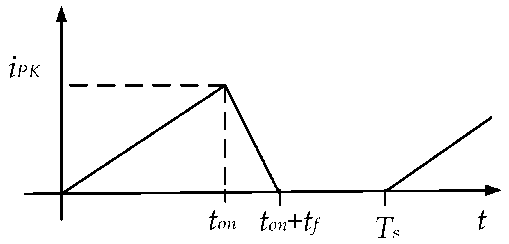
Figure 6 shows
iLPFC in one high-frequency cycle where
ton is the conduction time of switch
S2 and
tf represents the fall time of
iLPFC. The duty ratio
D is defined as:
where
Ts is the period of the switching frequency. At DCM operation, the peak value of the inductor current can be expressed as:
From Equation (10), relationship between
ton and
tf can be described as Equation (11).
The average value of
iLPFC over a high-frequency cycle is given, and can be expressed as [
23]:
where the index
k is defined as:
The input current is equal to the average value of the PFC inductor current, and can be expressed as:
The input power can be obtained by taking the average of the product of the input voltage and current over one line-frequency cycle. From Equations (8) and (14), the input power can be derived as [
24]:
where
y is expressed as:
From Equations (15) and (16), the inductance of
LPFC can be calculated by using Equation (17).
where
Po and
η represent the output power and circuit efficiency, respectively.
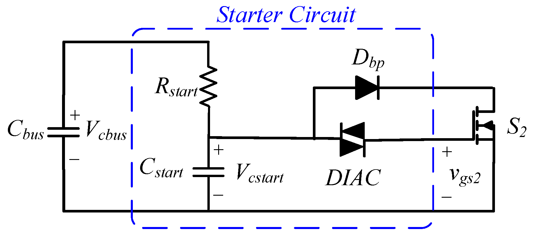
2.4. Starter Circuit
In the self-excited circuit, a circuit starter is indispensable to initialize the operation.
Figure 7 shows the starter circuit used in the developed LED drive. The starter circuit is connected in parallel with the dc-bus capacitor
Cbus with a simple resistor-capacitor (RC) circuit. Prior to the action of the starter, the dc-bus voltage
VCbus charges toward
Cstart via
Rstart. With the time constant being represented by Equation (18), when the exponentially increasing voltage on the starting capacitor
Cstart reaches the breakover voltage of DIAC, the DIAC conducts and the power switch is triggered. As soon as
S2 commences to conduct, the resonant process begins. However, to avoid
VCbus continually charging
Cstart, a bypass diode,
Dbp, is connected across the power switch,
S2. Of course, the bypass current through
Dbp is drastically quantitatively smaller than the resonant current. To prevent the upper and lower switches from shooting through, the switching frequency needs to be far greater than the reciprocal of the time constant, as shown in Equation (19).
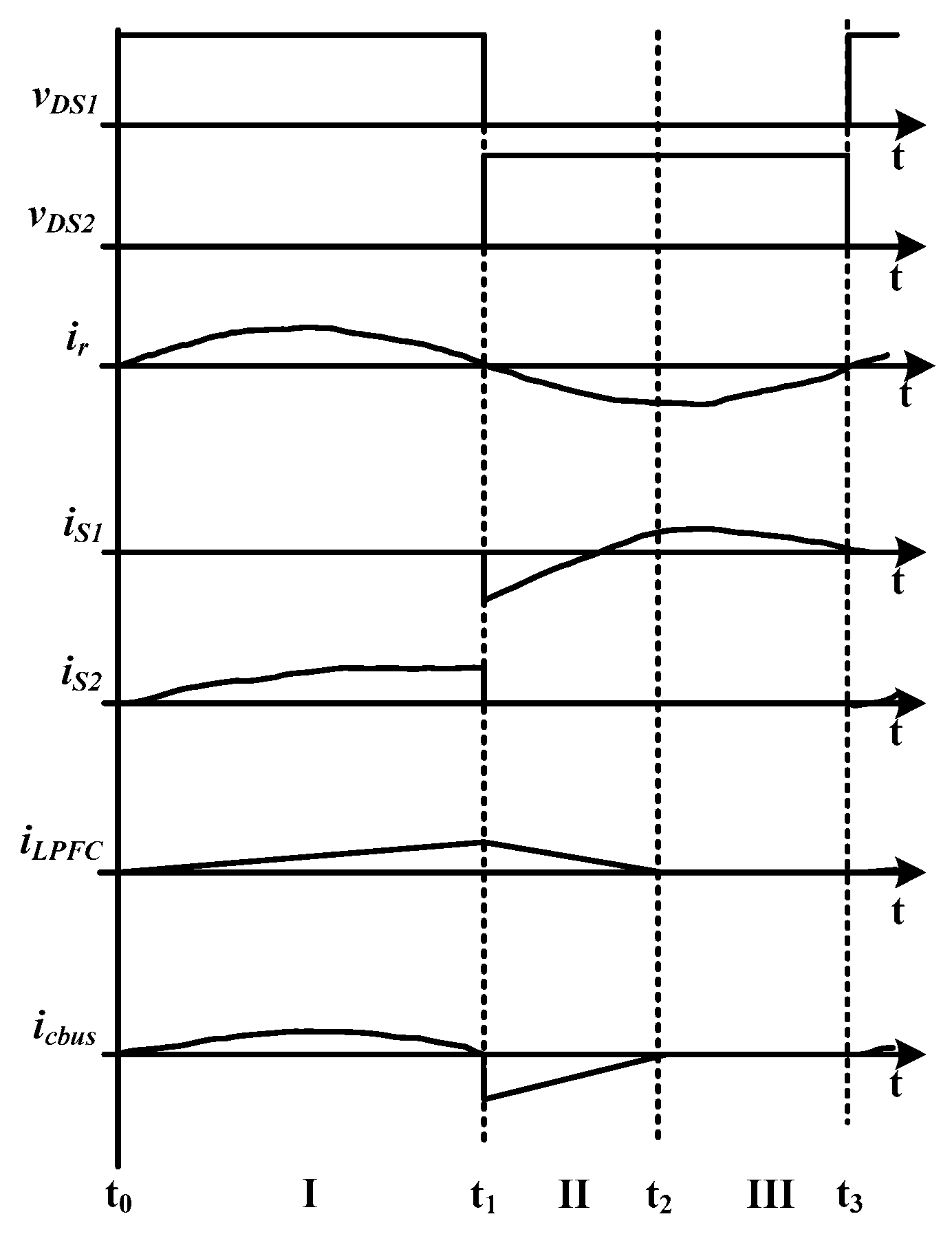
3. Circuit Analysis and Operation Modes
Figure 8 illustrates the schematic voltage and current waveforms of some key components. It can be inspected that both the PFC inductor current,
iLPFC, and the resonant current,
ir, flow through the power switch
S2. When the input square voltage crosses zero, the resonant current becomes zero as well.
The input voltage of the resonant circuit is a square wave, and can be described by the Fourier expansion.
When the quality factor of the resonant circuit is high enough, almost all the harmonic contents of
vAB will be filtered out by the resonant circuit. Only the fundamental current at the switching frequency is present in the load resonant converter [
22]. At steady-state operation, the voltage across the secondary winding is equal to the output voltage, and the load (including the output capacitance
Co) is fed by a rectified sinusoidal current source. The impedance across the secondary winding is equal to the resistance of the LED string (
RLED).
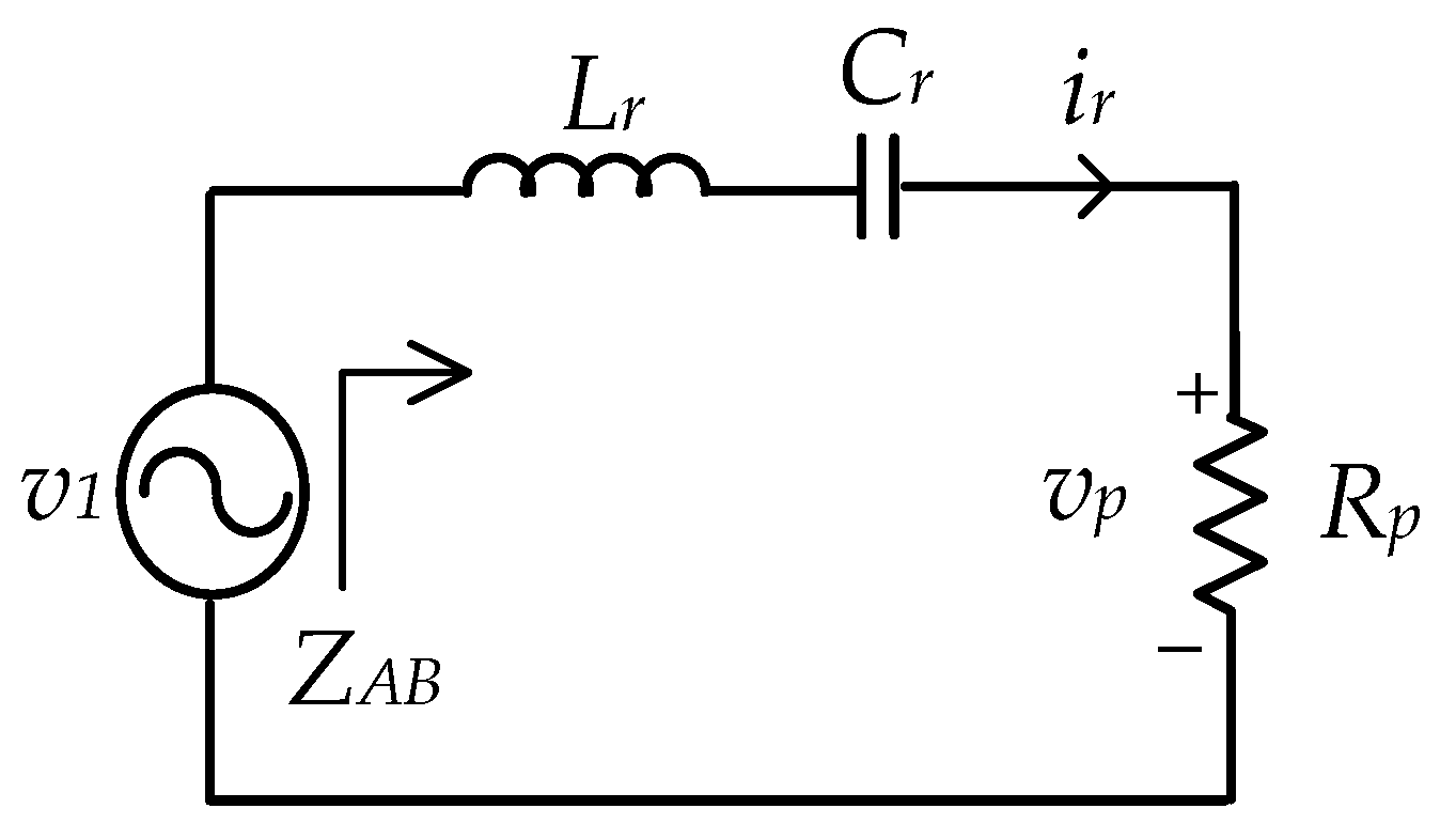
Figure 9 shows the equivalent circuit of the resonant circuit, where
v1 represents the fundamental voltage of
vAB. From Equation (20), the root-mean-square (rms) value of the fundamental voltage is equal to:
The impedance of the resonant circuit can be expressed as:
Under this circumstance, the resonant current is sinusoidal, and can be expressed as:
From Equation (23), the resonant current would theoretically be zero in the case of failure and the load would go open circuit. However, in practical terms, a small current is there if the mutual inductance of the transformer is considered. On the contrary, in the case of failure where the load goes short circuit, the primary winding and the excited windings will all become short-circuited. Thus, both power switches will not be energized and the circuit will remain turned off. Besides, the LED current is not regulated in the proposed circuit since a self-excited control mechanism is used.
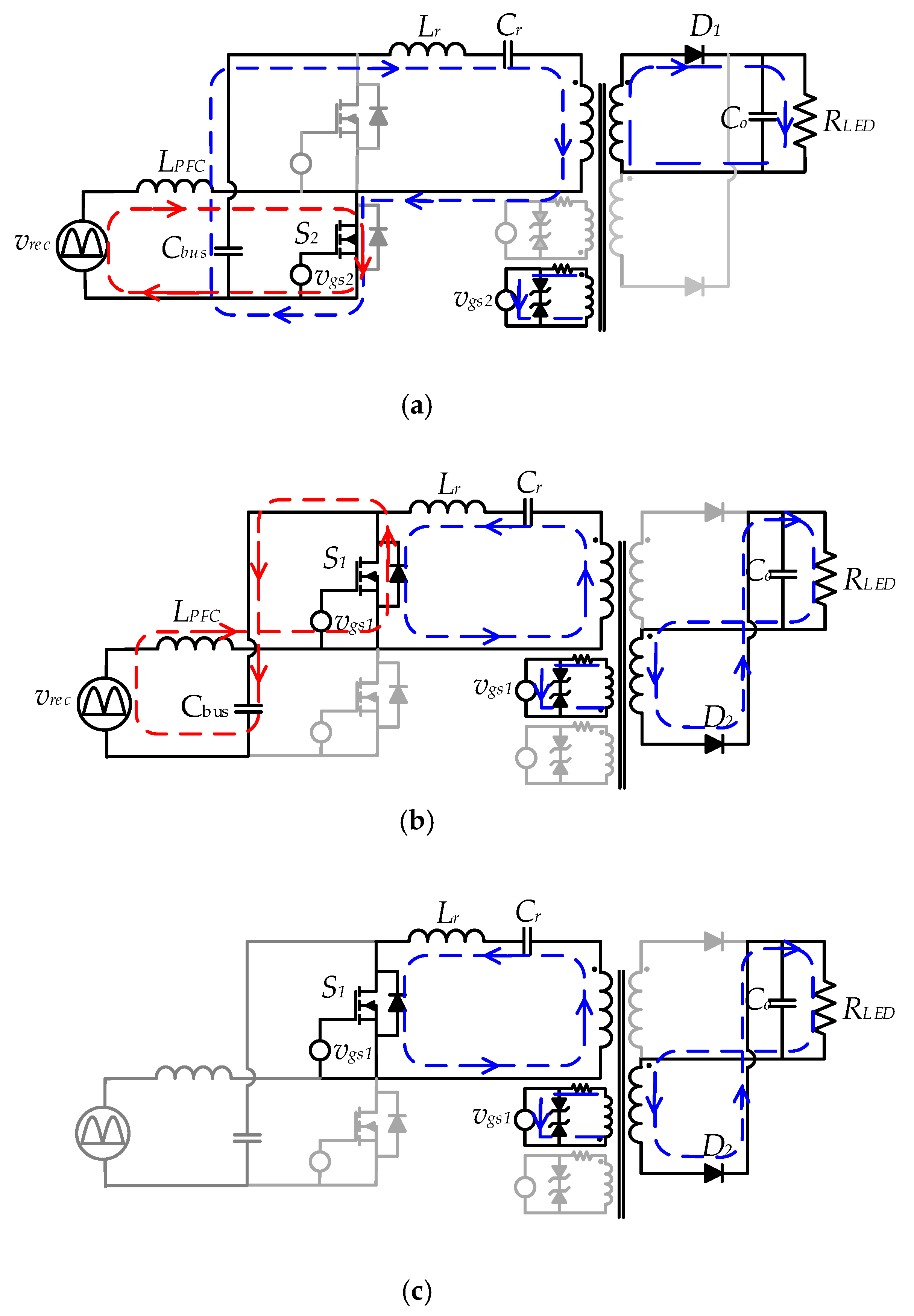
At a steady state, the circuit operation can be divided into three modes in every high-frequency cycle. The current loops of each operation mode are shown in
Figure 10, where
vrec represents the rectified voltage of the input line. As soon as the lower-arm power switch
S2 starts successfully, the circuit operation initiates. The operating modes are described below.
3.1. Operation Mode I (t0 − t1)
In this mode,
S2 conducts,
S1 is off, and the rectified input voltage
vrec is across the boost inductor
LPFC. The PFC current
iLPFC flows through
S2 and increases linearly, as written in Equation (24).
In addition, the dc-bus voltage
Vcbus is across the input of the resonant circuit and supplies a nearly sinusoidal resonant current,
ir. The
ir is positive and energizes the center-tapped transformer, as indicated in
Figure 10a.
3.2. Operation Mode II (t1 − t2)
The equivalent circuit of Mode II is shown in
Figure 10b. This mode starts as soon as the resonant current,
ir (via the center-tapped transformer) decreases to zero, and the primary winding then induces a back electromotive force (emf) and result in the conduction of power switch
S1, along with the turn-off of switch
S2. The current
iLPFC reaches a peak value at the beginning of Mode II. Since
S2 is off, the current
iLPFC diverts from
S2 to
DS1 to charge the dc-bus capacitor
Cbus. The voltage across
LPFC is equal to
Vcbus minus
vrec, which is negative, meaning that
iLPFC decreases linearly.
In this mode the current ir is negative. Simultaneously, the resonant tank releases energy to the load.
3.3. Operation Mode III (t2 − t3)
The equivalent circuit of Mode III is shown in
Figure 10c. This mode starts when the current
iLPFC decreases to zero. In this mode,
S1 keeps conducting. The resonant current continually supplies energy via the center-tapped transformer to the output.
5. Experimental Results
A prototype circuit was built and tested. The circuit parameters are shown in
Table 2, and the prototype circuit is shown in
Figure 11. The experimental apparatuses consisted of an oscilloscope (Lecroy HDO4034, New York, NY, USA), voltage probes (Cybertek DP6150A, Shenzhen, China), current probes (Cybertek CP8030A, Shenzhen, China), and a power quality analyzer (Precision International Corp. PA-750B, New Taipei City, Taiwan).
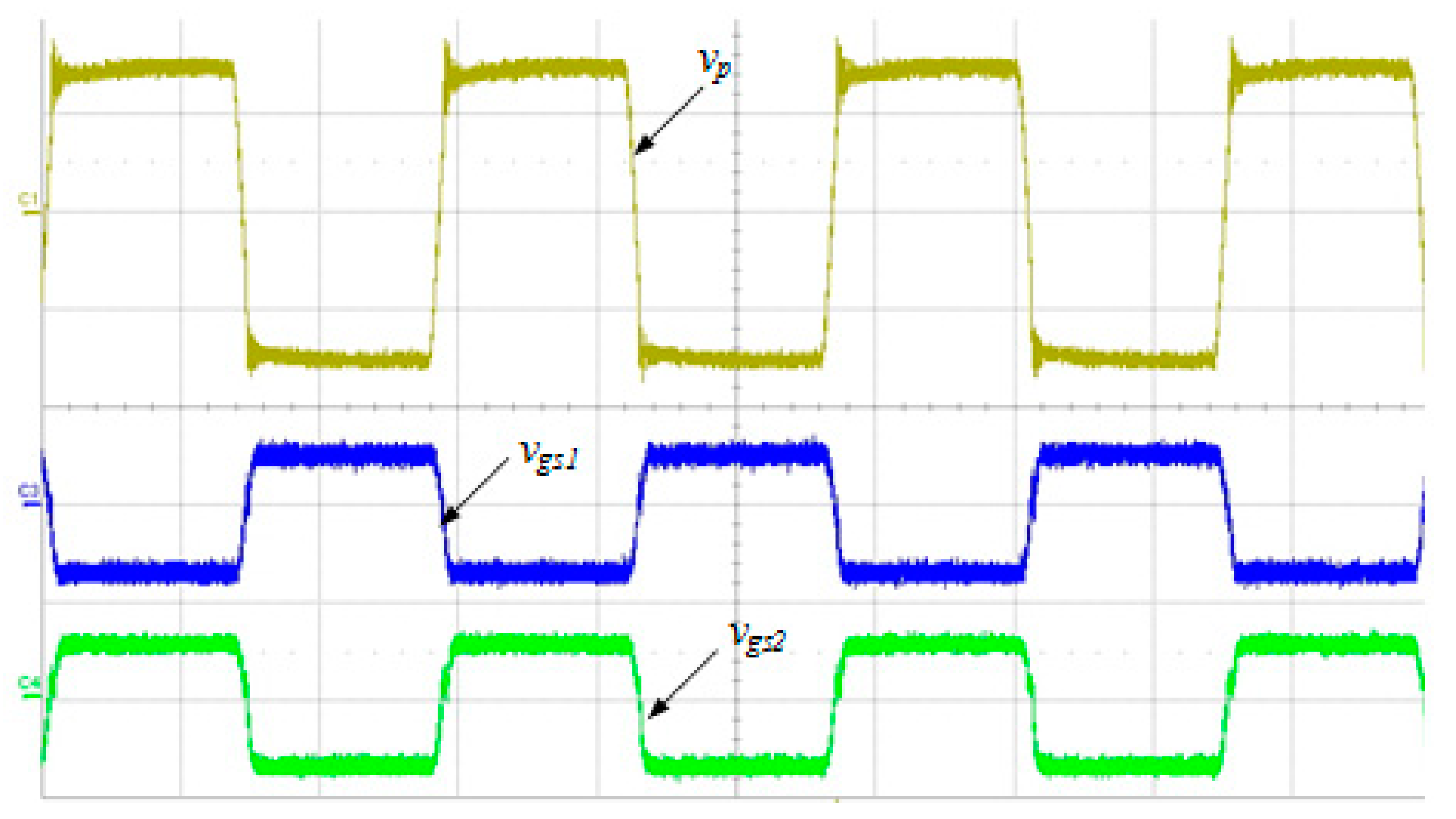
Figure 12 shows the measured voltage waveform on the primary winding and the self-excited windings of the center-tapped transformer. It can be seen that the self-excited voltage
vgs1 and
vgs2 are in phase with the primary voltage
vp. Obviously, the driving voltages
vgs1 and
vgs2 are symmetrically displaced by 180°. Hence, the switching frequency of the power switch could be the same as the resonant frequency of the resonant converter.
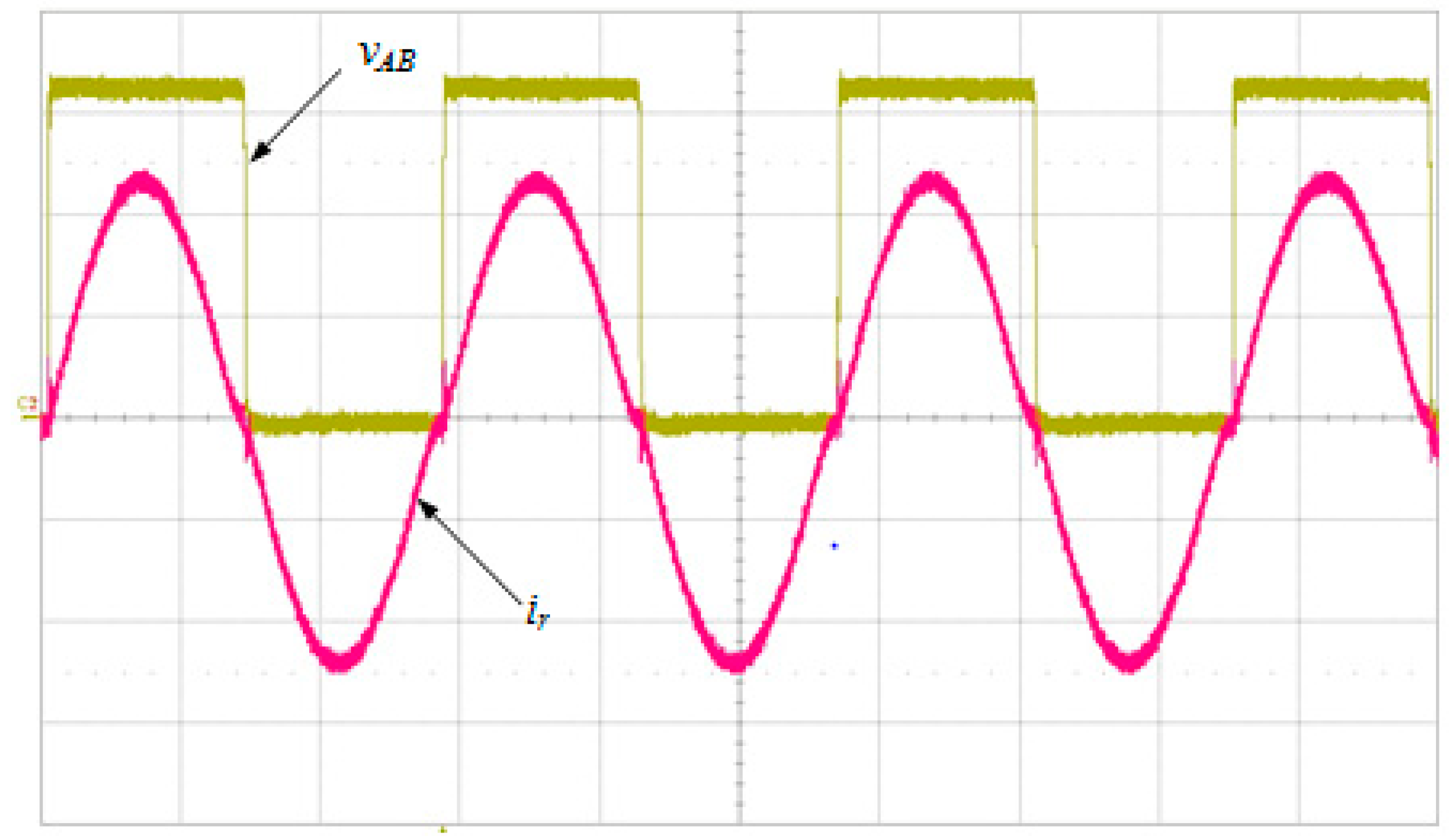
Figure 13 shows the input voltage of the resonant converter
vAB and the resonant current
ir. It demonstrates that
ir is in phase with
vAB. This marks the equality of the resonant frequency and switching frequency, i.e.,
fr = fs.
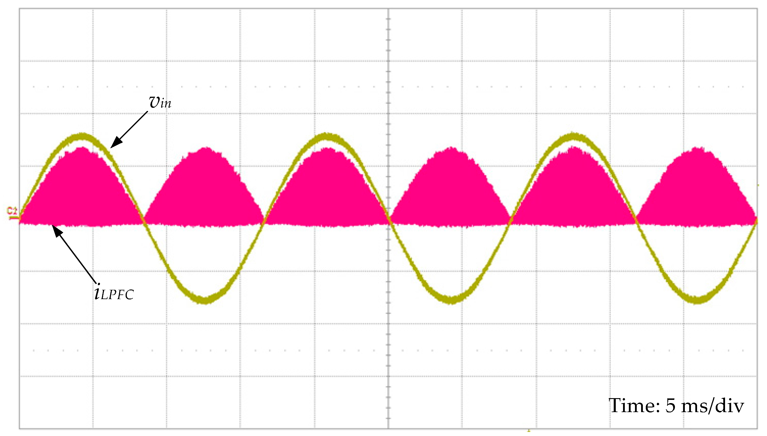
Figure 14 shows the waveforms of the input line voltage and the PFC inductor current
iLPFC. It reveals that the envelope of
iLPFC is in phase with the low-frequency input line voltage.
Figure 15 shows the waveforms of
iLPFC and the voltage across the power switch
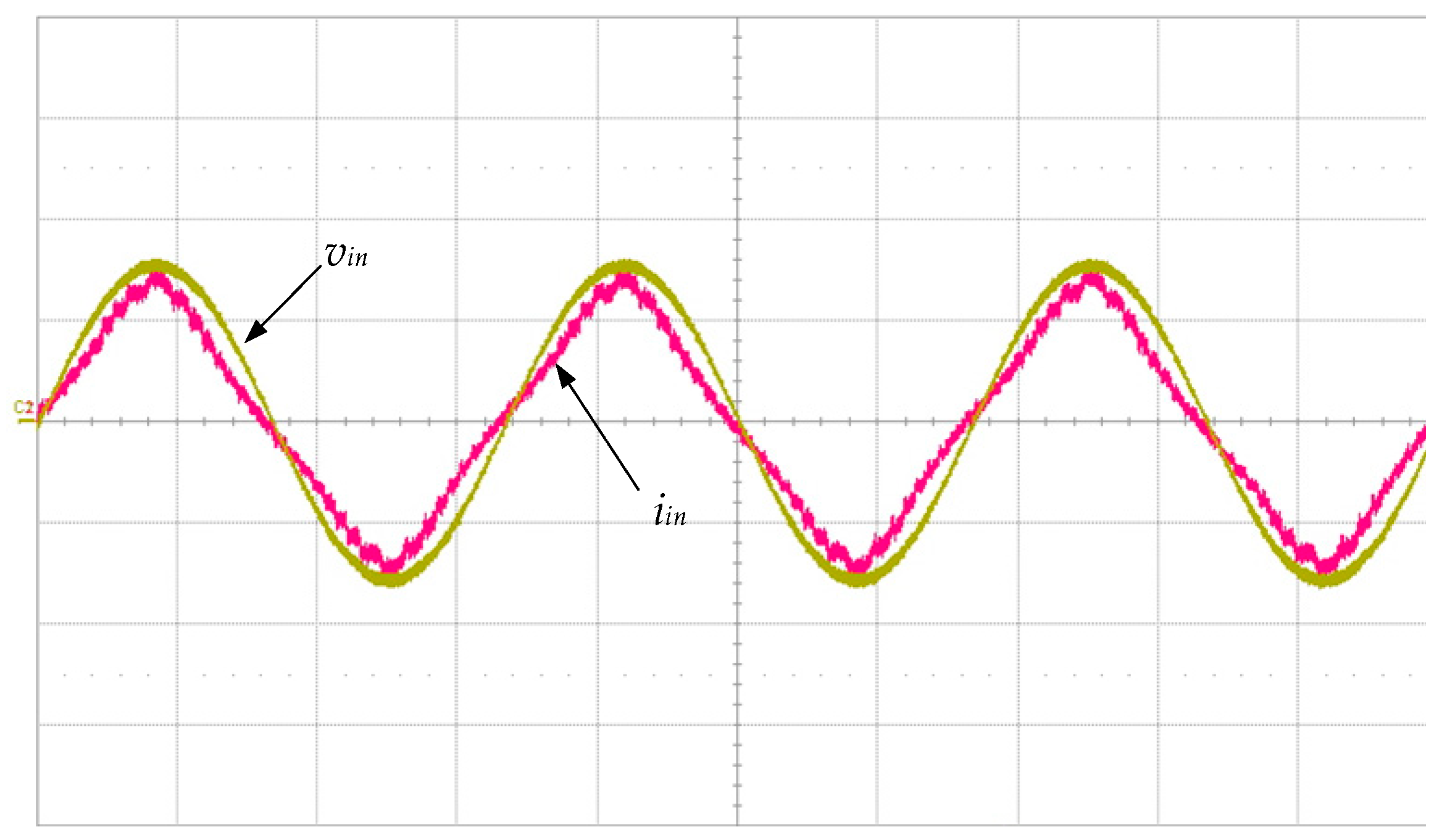
S2. It indicates that the PFC converter operates at BCM when the input line voltage is at the peak value, while it operates at DCM elsewhere. The waveforms of the input line voltage and current are shown in
Figure 16. It can be seen that the input current is in phase with the line voltage. The measured unity power factor and total current harmonic distortion (THDi) is 0.98 and 10.2%, respectively. It is seen that the input current is close to a triangle waveform. In this proposed circuit, the power switches are operated at a fixed switching frequency and fixed duty ratio (
D = 0.5). Since the boost-typed PFC operates at DCM, the peak value of the inductor current is proportional to the rectified input voltage, i.e., the envelope of the inductor current would be a sinusoidal waveform. Theoretically, the average value of the rising portion of the inductor current within a high-frequency cycle is also sinusoidal. Nevertheless, the duration of the inductor current dropping from peak to zero is not constant. The higher the input voltage, the longer the declining duration. When the PFC operates at the time when the input voltage is at the peak of a sinusoidal waveform, the average value of the inductor current would be much higher than the peak. This is why the current waveform looks triangular.
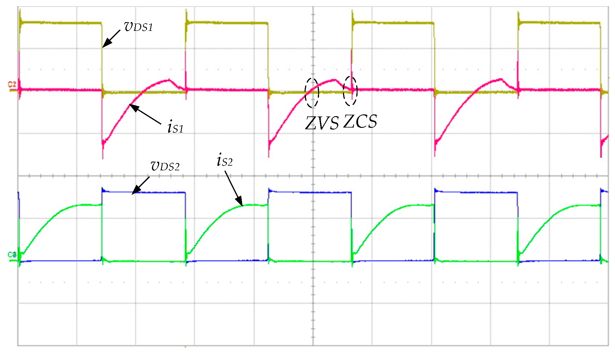
Figure 17 shows the voltage and current waveforms of the power switches. Since the switching frequency is identical to the resonant frequency,
S1 can be turned off at zero current. Besides, as mentioned in operation Mode II, the PFC inductor current diverts from
S2 to
DS1 as soon as
S2 is turned off. In this way, the voltage across
S1 is clamped to near zero volts. It helps the power switch
S1 to be turned on at zero voltage. Theoretically, the power switch
S2 should be turned on at zero voltage when the resonant circuit presents a resistive characteristic. Nevertheless, it is shown that a spike current happens when
S2 is turned on, meaning that
S2 does not achieve ZVS operation.
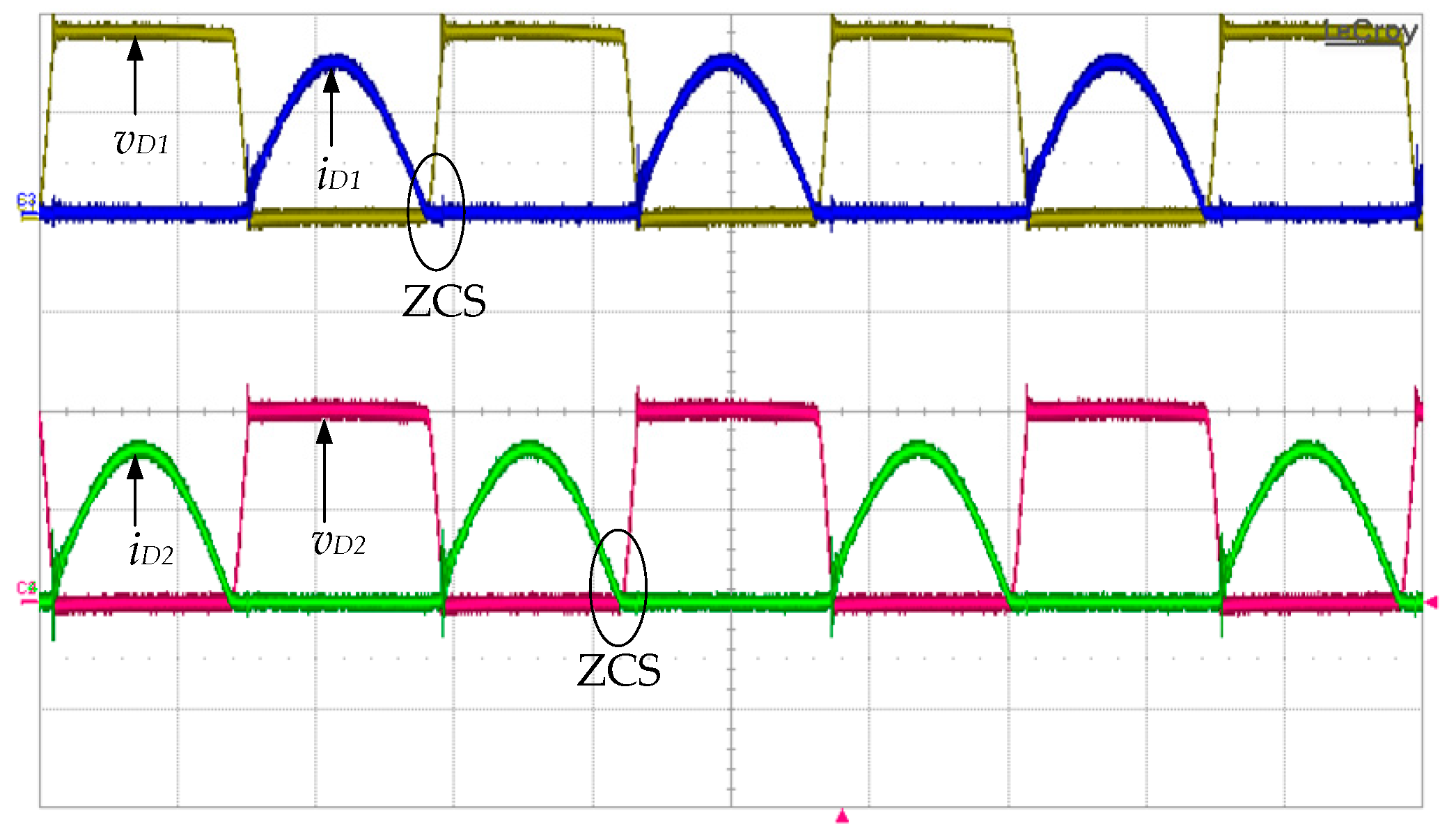
At the output side of the developed circuit, the ZCS performance has been accomplished by inspecting the relationship between diode voltage waveforms and diode current waveforms on both
D1 and
D2.
Figure 18 obviously shows that the current of the output diodes naturally fall to zeros prior to the moment that the transformer secondary windings switch. It means that diodes
D1 and
D2 can operate at ZCS, resulting in a zero-recovery current and low turning-off losses.
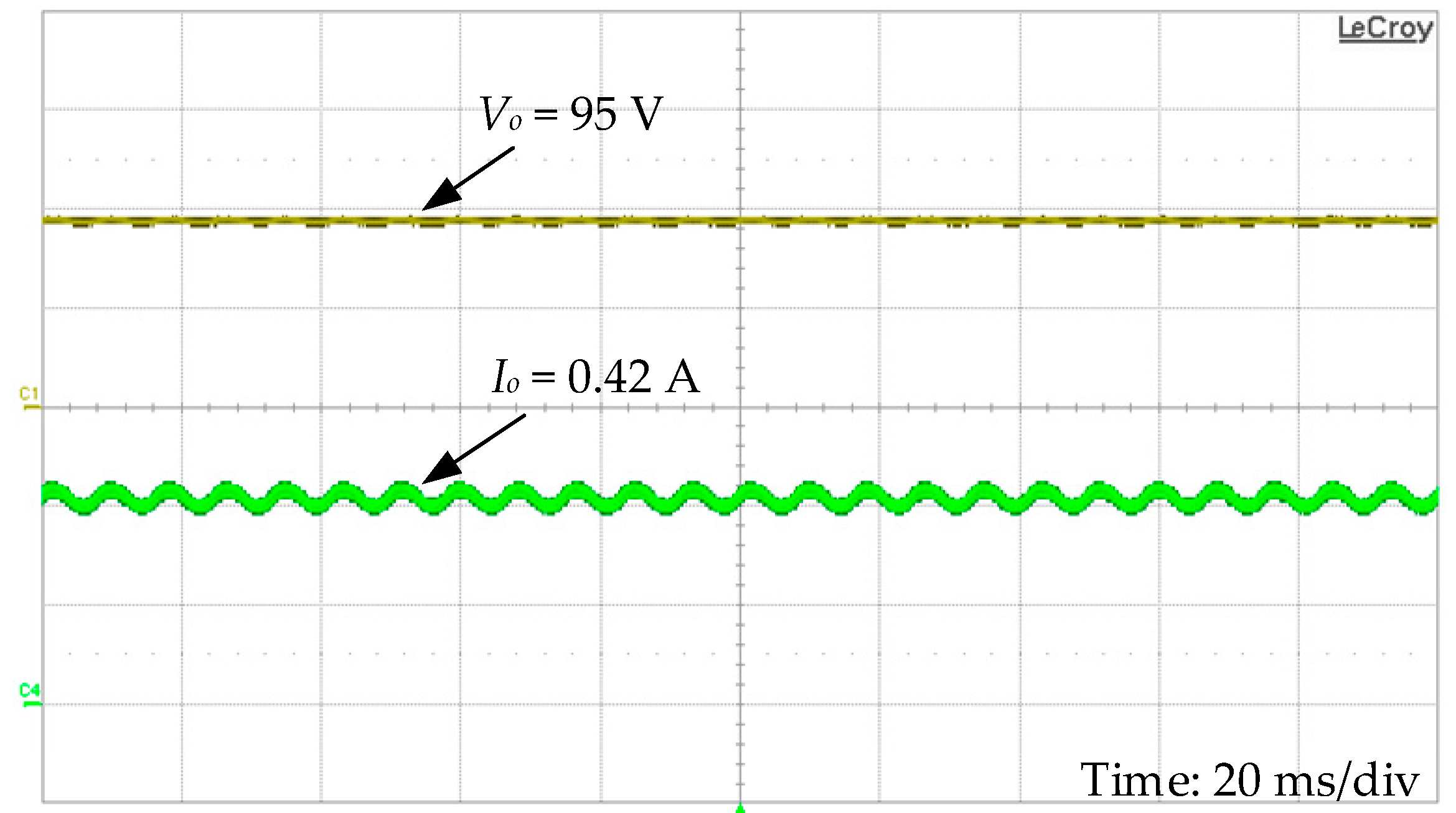
Figure 19 shows the waveforms of the output voltage and current, and as displayed, there are both high-frequency and low-frequency ripple components in the voltage and current. The measured average voltage and average current are 95 V and 0.42 A, respectively. The circuit efficiency is 92.2%. The measured values are consistent with the theoretical prediction, and the peak-to-peak voltage ripple is 560 mV, while the peak-to-peak current ripple is 46 mA. The ripple factors of the voltage and current are 0.6% and 10.9%, respectively.
6. Conclusions
In this research, a synchronized, self-excited control for a single-stage LED driver has been developed. The proposed circuit topology was derived by integrating a boost converter which functioned as a PFC, as well as a series resonant converter outputting a dc voltage to drive an LED string, which helps to save the number of power switches and their corresponding control circuits. In using this novel, self-excited driving approach, the proposed circuit does not need to use an integrated circuit. In addition, the components used to build a dc voltage for an integrated circuit could be saved. Because the driving voltages of the power switches are synchronized with the resonant current of the resonant circuit, the switching frequency and resonant frequency are identical, meaning that the power switch of the upper arm can operate at both ZVS and ZCS. However, the power switch of the lower arm cannot operate at ZCS, since it is shared by the PFC converter to help both the PFC inductor current and the resonant current to flow. Besides, the rectifying diodes at the output side possess the zero current cut-off characteristics. The high power factor and low THDi allow, by design, the boost-typed PFC converter to operate at DCM. The measured power factor and THDi are 0.98 and 10.2%, respectively, and the overall performance efficiency is 92.2%.


