Article

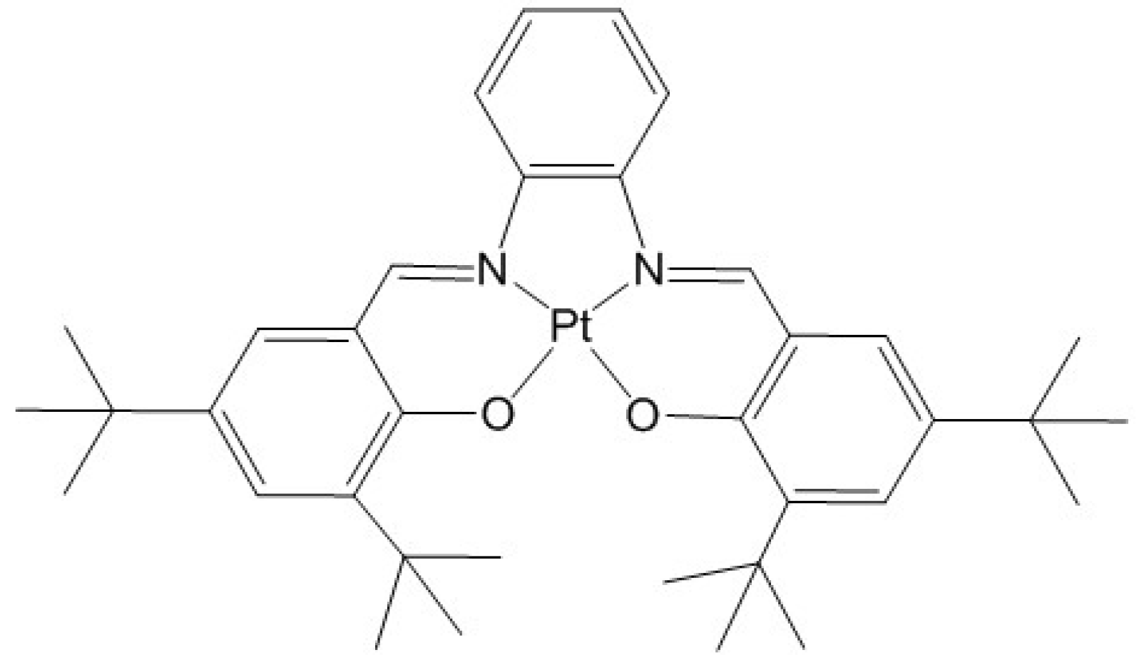
Application of [Pt(II)(Tetra-Tert-Butylsalophen)] Complex within Organic Devices: Deep Red Emission, Bistable Light-Emitting Diodes and Operational Stability

1
LAPLACE (Laboratoire Plasma et Conversion d’Energie), Université de Toulouse, CNRS, F-31062 Toulouse, France
2
LCC (Laboratoire de Chimie de Coordination), Université de Toulouse, CNRS, F-31077 Toulouse CEDEX 4, France
3
Laboratoire de Chimie et Physique Quantiques, Université de Toulouse, CNRS, F-31062 Toulouse, France
*
Author to whom correspondence should be addressed.
Appl. Sci. 2018, 8(5), 762; https://doi.org/10.3390/app8050762
Submission received: 9 February 2018 / Revised: 27 April 2018 / Accepted: 30 April 2018 / Published: 11 May 2018

Abstract

:
This paper focuses on the Negative Differential Resistance (NDR) we observed on organic light-emitting diodes (OLEDs) using [Pt(II)(tetra-tert-butylSalophen)] as host, since this Pt(II) complex displays a deep-red emission (λmax = 660 nm). Electrical characterizations of monolayer devices have shown that doping Tris-(8-hydroxyquinoline)aluminum (Alq3) as matrix emissive layer with this complex, leads to the modulation of the charge transport properties highlighted by Negative Differential Resistance (NDR). Upon electrical driving stresses, the conductivity of active layer can be switched between two electrical states (ON and OFF) with a figure of merit higher than 103. By adding an electron-blocking layer, we demonstrated that the NDR trend is closely related to negative charge accumulation within Alq3 leading to the modification of electronic properties in the vicinity of anode/active layer interface. The NDR phenomenon is interpreted in terms of space charge polarization (SCP) linked to charge trapping/untrapping mechanism as a consequence of the polarization/depolarization of the Pt(II) complex. Under electrical driving stresses, the performance of the devices which include the Pt(II) complex, are stabilized. A schematic model is proposed to depict the SCP responsible for NDR and decrease-resetting behaviors observed in these devices.

1. Introduction

Metal organic complexes have been investigated and have shown promising optoelectronic features for energy conversion such as electroluminescence or photoelectricity [1]. Phosphorescent complexes including d6 or d8 metal surrounded by π-conjugated ligands have been used for optimization of Organic Light-Emitting Diodes (OLEDs) [2,3]. Among these ligands, Schiff base ligands are attractive because their structure can be easily modified [4]. By using such phosphorescent dyes in host fluorescent matrix, both singlet and triplet excited states participate to light emission of electroluminescent devices [5,6] and a 100% internal quantum yield can be theoretically achieved.
Depending on the device structure and operating mode, the lifetimes of OLEDs produced in laboratories can reach ten thousand hours [7,8,9,10,11,12]. Nevertheless, degradation mechanisms occur and display through a modification of the emission color and/or a reduction of the driving current and the luminance. The effect of aging leads to a progressive increase in impedance during the operation of OLEDs and in order to maintain a constant current, the bias polarization has to be raised more and more [13]. However, it was observed that half lifetime (the time for which the decrease in luminance is 50% from the initial value) and the initial decay are closely related to the amount of non-emissive triplets in emissive layer [9,10]. Thus, among the degradation mechanisms that should be controlled, the management of the non-emissive excitons in the active layer seems to be a key factor in aging of devices. It was observed that doping an emissive layer with a metal complex affects the charge transport properties of emissive layer and device stability [7,14]. In this work, we focused on the study of [Pt(II)(tetra-tert-butylSalophen)] used as phosphorescent dye. In fact, this complex displays a deep-red emission (λ max = 660 nm). We present the optical and electrical features of Pt(II) complex based organic devices obtained by Physical Vacuum Deposition (PVD).
The paper is organized as follows: we first discuss the optical features in a host-guest system of [Pt(II)(tetra-tert-butylSalophen)] embedded within a Tris-(8-hydroxyquinoline)aluminum (Alq3) layer [15]. Then, we analyze the electrical features of Pt(II) complex based devices. Finally, the stability measurements are studied and discussed in relation with the electrical features of the Pt(II) complex based layer. Space Charge Polarization (SCP) mechanism is proposed for the interpretation of the electrical characteristics of the devices.

2. Materials and Methods

[Pt(II)(tetra-tert-butylsalophen)] was prepared as previously reported [15]. The devices were fabricated by successive vacuum depositions (<10−5 mbar) of the organic layers and a cathode on a glass substrate covered by a semitransparent electrode. Patterned Indium Tin Oxide (ITO) coated glass substrates from Kintec (100 nm and sheet resistivity about 14–18 Ω/sq at room temperature) were used as a transparent anode. A 20-nm thick of Poly(3,4-ethylenedioxythiophene) polystyrene sulfonate layer (PEDOT:PSS) (CLEVIOS PJET HKV2 charge GSD from Heraeus) was spin coated on the top of ITO glass substrates and was annealed at 100 °C for 10 min. PEDOT:PSS was used as hole injection layer. Thin layers of N,N′-Di(1-naphthyl)-N,N′-diphenyl-(1,1′-biphenyl)-4,4′-diamine (NPD) and Alq3 (sublimated grade purchased from Kintec) were used as the hole (HTL) and electron (ETL) transporting layers respectively. A 150-nm thick calcium layer (99.99% from Aldrich) was used as the cathode. The doping of emissive layer with 5% of Pt(II) complex was performed by co-evaporation of Alq3 as host material at a rate of 1 Å/s and the Pt(II) complex labeled [Pt] at a rate of 0.055 Å/s. The thickness of organic films was determined in situ by quartz-crystal monitor. The thickness and the homogeneity of the resulting films were controlled by profilometry (TENCOR P2 stylus profilometer) and AFM measurements (Dimension TM 3100 Atomic Force Microscope (Digital Instruments)). Monolayer device structures were: ITO/PEDOT:PSS/emissive layer (EML)/Ca. With Alq3 doped with 5% [Pt] as EML. In bilayer devices, NPD was added between the ITO/PEDOT:PSS anode and EML. The active area of the devices was 18.3 mm2. Schematic and energy band diagrams with the energy levels of the OLEDs are illustrated in Figure 1a,b, respectively. The The highest occupied molecular orbital (HOMO) and lowest unoccupied molecular orbital (LUMO) levels were previously estimated from cyclic voltammetry measurements [15].
Characterizations of the OLEDs were obtained under inert atmosphere. Current-luminance-voltage (J-L-V) measurements were carried out by using current-voltage source (Keithley, model 2450). The electroluminescence (EL) spectra and the luminance of the OLEDs were measured by using a Spectroradiometer (JETI SpecBos 1201). For stability measurements, the current and the luminance of devices were recorded every 30 s at a constant driving voltage of 8 V. The stability of the following structures were studied: ITO/PEDOT/NPD(55 nm)/Alq3(85 nm)/Ca and ITO/PEDOT/NPD(55 nm)/Alq3:5% [Pt] (85 nm)/Ca labeled as non-doped and doped devices respectively.

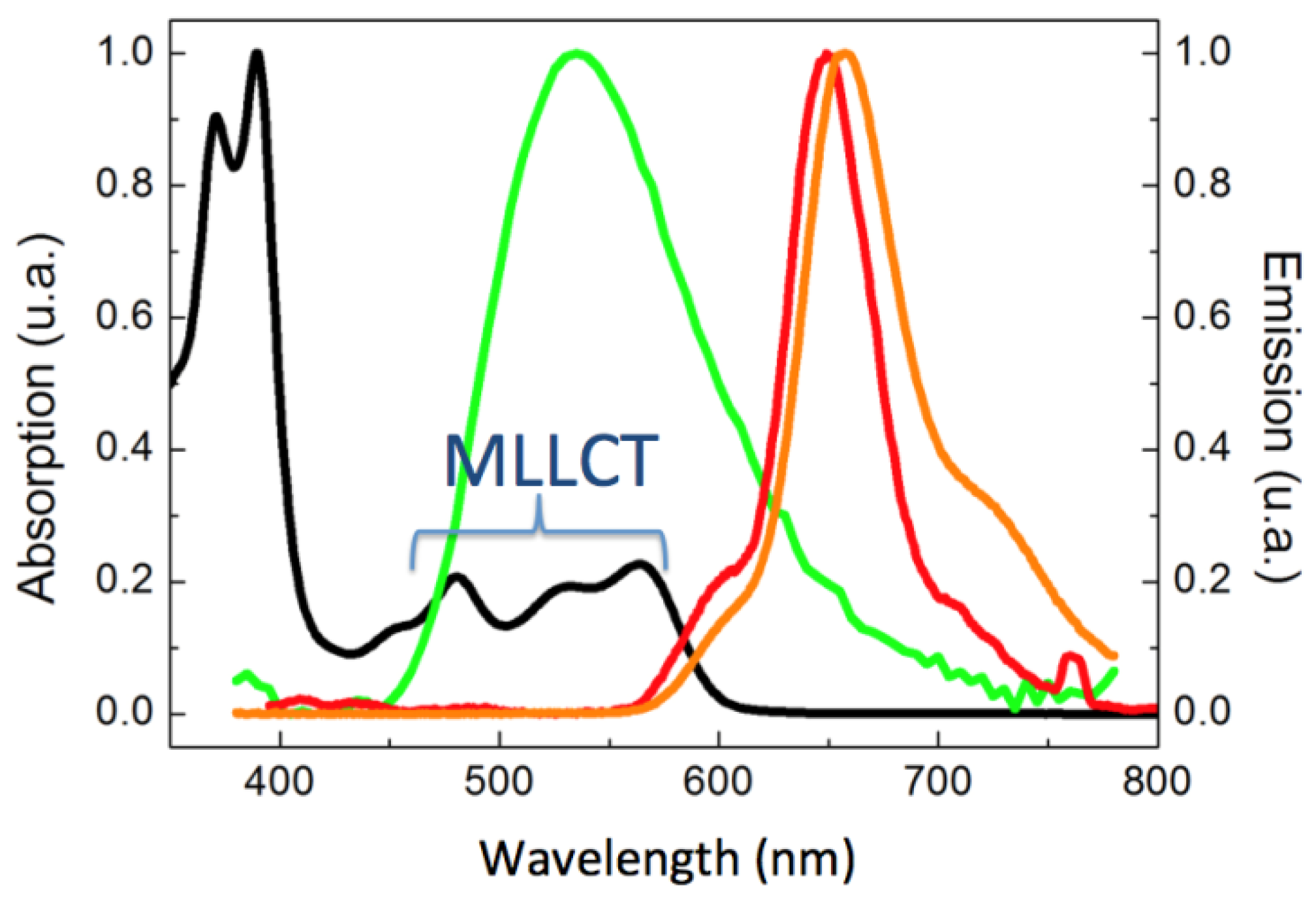
3. Results and Discussion

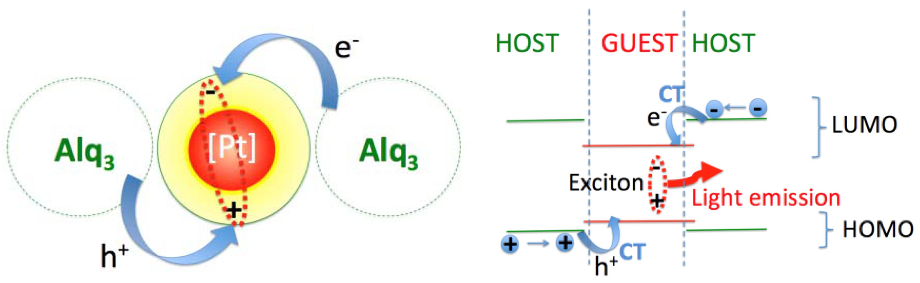
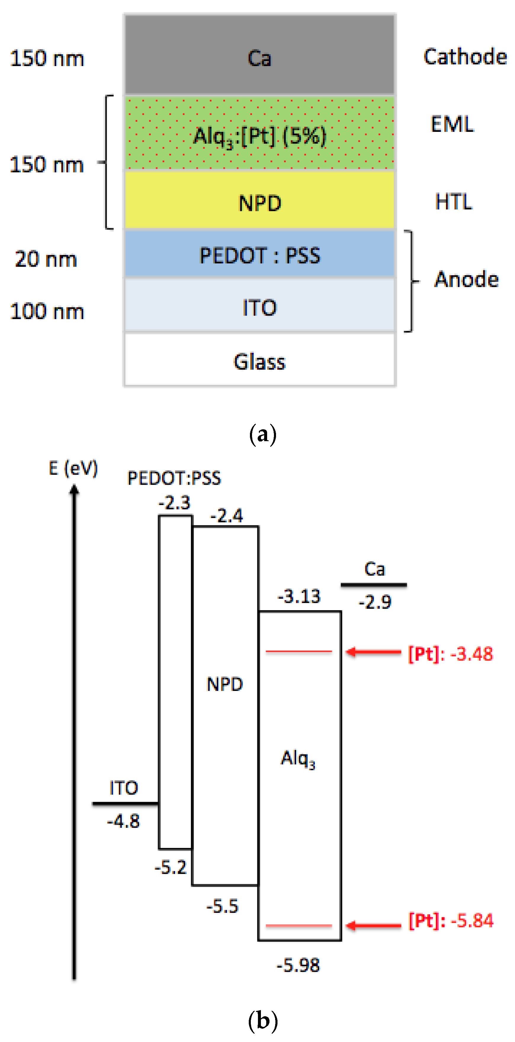
3.1. Host-Guest System

Based on C. Che et al. research on phosphorescent Pt(II) Schiff Base complexes [16], we synthetized [Pt(II)(tetra-tert-butylsalophen)] named [Pt] (Scheme 1) which is thermally stable (Td = 390 °C). Time-dependent density functional theory (TD-DFT) calculations [15] have been performed in order to assign the different electronic transition of [Pt].
[Pt] exhibits absorption bands in the range of 400–600 nm attributed to metal-ligand-ligand charge transfer (MLLCT). After excitation at λex = 390 nm, an emission band was observed between 575 nm and 750 nm (λmax = 660 nm) (Figure 2). Alq3 emission spectrum overlaps with the absorption spectrum of [Pt] and should favor an efficient energy transfer from Alq3 to [Pt].
The doping rate of the emissive layer plays a key role in the devices efficiency and color emission. It was demonstrated that the device efficiency increased with a concentration of platinum (II) dopant, up to 5 wt % or 6 wt % depending on the platinum(II) complex [16]. By considering a 6 wt % concentration of [Pt] (with Alq3 number density ~1021 cm−3 [17]) and by assuming that the Pt-complexes do not aggregate, the number density of Pt-complex is estimated at about 6.1019 [Pt]/cm3 and the average distance between neighboring complexes at ~3 nm. Thereby, the effective distance over which the energy transfers between complexes (estimated at 3 nm) would be higher than the radius of triplet-triplet annihilation (<1 nm through Dexter mechanism) [18,19,20]. Furthermore, the steric hindrance between adjacent molecules induced by the tert-butyl substituents of [Pt] tends to limit the formation of [Pt] aggregates and hence reduces aggregation-induced phosphorescence quenching in thin solid film [15,16]. Consequently, doping rate of [Pt] is fixed at 6 wt % to maximize the performance of the devices.
The host-guest confinement methodology was used to modulate and to improve the electroluminescent properties of the devices (Figure 3). The monolayer device exhibited a deep red emission band attributed to the [Pt], whereas the green emission of Alq3 was vanished, implying an efficient energy transfer from the host to the guest. In our previous investigation [15], it was observed that during OLED polarization, some of charges were directly captured by the dye to form an exciton. HOMO/LUMO levels of [Pt] (estimated at −5.84 eV and −3.48 eV (Figure 1) respectively from electrochemistry measurements) are within the electronic gap of Alq3 matrix (with HOMO level: −5.98 eV and LUMO level: −3.13 eV); involving that exciton formation, arising from charge transfer mechanism, would be confined on [Pt] (Figure 3) by a charge transfer (CT) process. The emission process can be described by (i) migration of charge carriers (holes and electrons) within the host layer (ii) CT from the host to the guest (iii) exciton formation on [Pt] (iv) radiative recombination of triplet states.

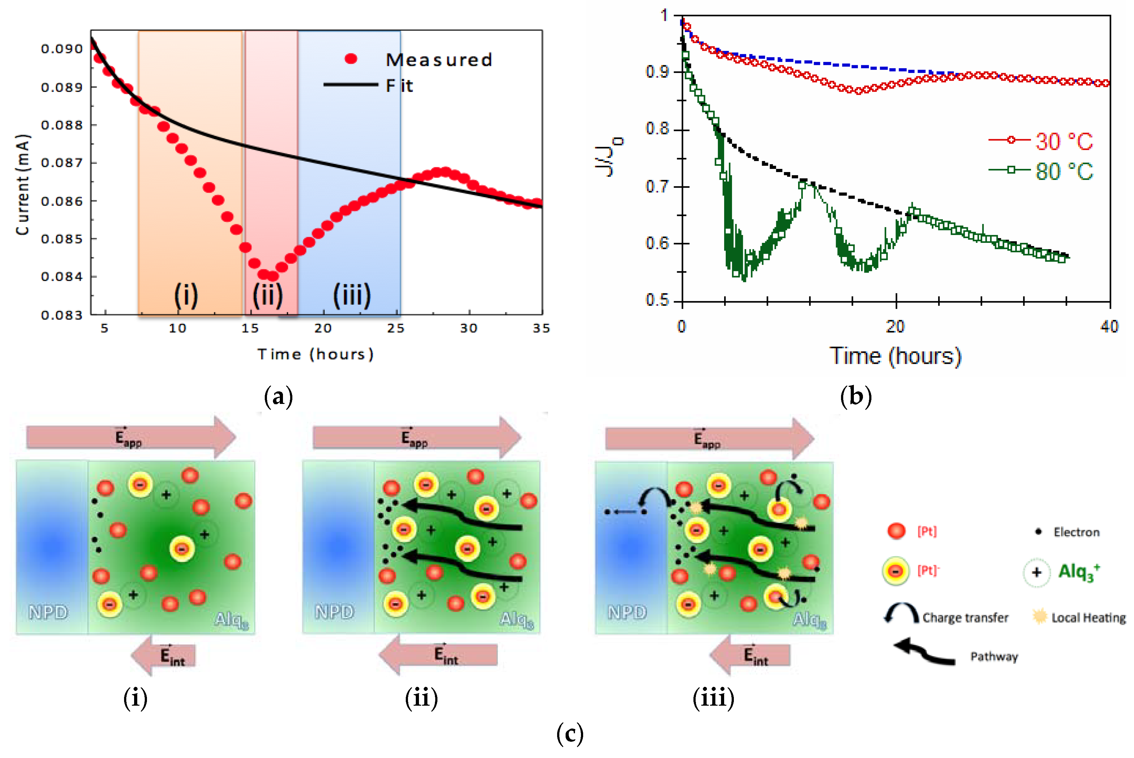
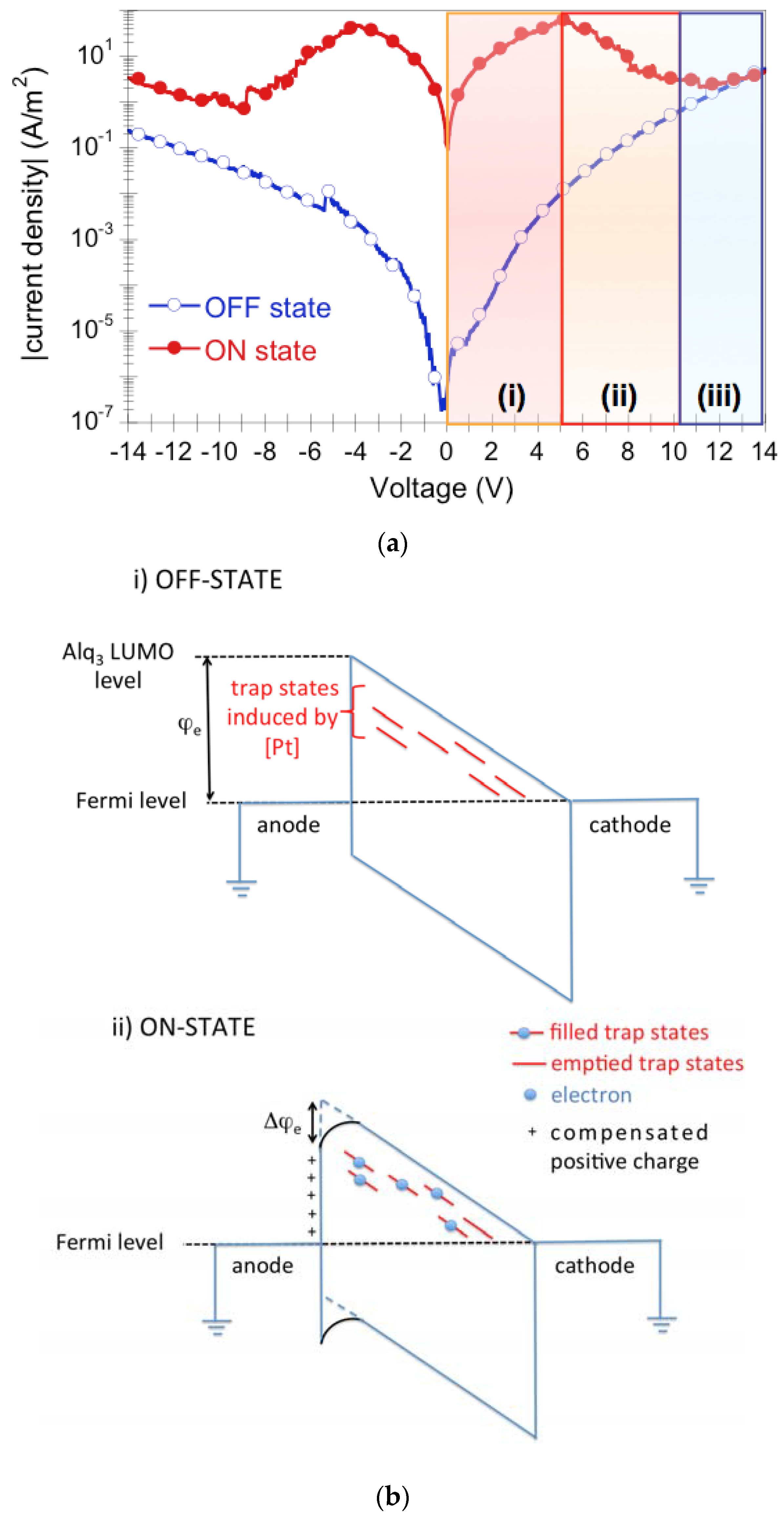
3.2. Negative Differential Resistance

The effect of [Pt] on the charge transport in the Alq3 layer was investigated from J-V characteristics in a monolayer device (Figure 4a). After performing sweeping voltage from 0 V to +14 V, the current abruptly increased in the range of 0 to 5 V then decreased in the range of 5 to 8 V. The peak of current is obtained for an applied voltage of 5 V. This shape of J-V is characteristic of negative differential resistance (NDR). It was only observed on [Pt] doped devices. By performing ten successive sweeping cycles (positive poling), the repeatable NDR behavior was observed with an increase in current peak. The intensity of this peak achieves a constant value after ten successive sweeping cycles (as shown in Figures S1–S3 of Supplementary Information). By performing negative poling (ten successive sweeping from 0 V to −14 V, as shown in Figures S2 and S3 of Supplementary Information), J-V characteristics recovered the initial shape, indicating that the electrical switching behavior is related to a reversible mechanism. At low voltage (below 8 V), the current could be switched between two electrical states: high-resistance state (OFF state) and low-resistance state (ON state). Thus, the current can be identified in three parts: (i) bistable area; (ii) Negative Differential Resistance (NDR) area and (iii) monostable area. An ON/OFF current ratio higher than 103 is achieved in the bistable area.
The origin of NDR features of devices could be assigned to the formation of electrically active defects introduced by the [Pt] within the Alq3 layer. Similar behavior was observed in devices based on organic layer doped by metal nano-clusters or fluorescent dyes [21,22,23,24,25]. It was proposed that charge accumulation within Alq3 layer would play a key role in the bistable trend and NDR properties [21]. At low voltage (<5 V), the switching conductance of the active layer can be due to localized electronic states leading to electron like-traps. The filling of these trapping states leads to the formation of Alq3+-[Pt] dipole resulting in space charge polarization (SCP) of active layer. The SCP can modify charge injection properties at the electrode/active layer interface; promoting conductive pathways or space charge field inhibition of charge injections [26].
The J-V characteristics carried out after positive poling show a transition in conduction mechanism from injection limited (OFF) to bulk limited (ON) suggesting a variation in the electric-field distribution between OFF and ON states. Due to the distribution of the LUMO levels (estimated at −3.13 eV and −3.48 eV for Alq3 and [Pt] respectively), the interface with the cathode is expected to be as ohmic contact for electrons (Figure 1b). Therefore, the asymmetrical J-V characteristics observed for OFF state could be explained by an energetic barrier at the interface (with the anode). That should result in injection-limited current in the device for negative applied voltages. After the positive poling, the charges are expected to be stored in the active layer due to the trap like behavior of [Pt] within Alq3 matrix. Consequently, the trapped charges within active layer should be compensated by charges from the metal electrode. A portion of the compensated charges could lead to band bending (Figure 4b) and that would likely lower the energetic barrier for electrons at the interface with the anode [27,28]. As a result, the current in the device increases to form the ON state in both polarity of the applied voltage (between −5 V and +5 V). It can be assumed that the injection properties of Anode/Alq3:[Pt] would be modified by charges trapped within Alq3:[Pt] layer.
The monolayer devices displayed poor luminance performance (below 10 Cd/m2) compared to bilayer structures with the NPD layer (inset of Figure 5). Bilayer devices with 10 nm and 55 nm thicknesses of NPD exhibited a luminance of 15 Cd/m2 and 35 Cd/m2 at 14 V respectively. The intensity of NDR is decreasing with the enhancement of NPD thickness (Figure 5). For monolayer devices, the stored charges on trapping states lead to the modification of both charge injection and conduction. For bilayer devices, NPD acts as electron blocking layer due to its lower value of LUMO level [29] and Alq3 as electron transport layer [30]. It can be inferred that the thin layer of NPD limits electron extraction from Alq3 to the anode and promotes hole injection. Consequently, the amount of stored negative charges is reduced due to hole injection leading to the decrease in NDR peak. That is confirmed by the enhancement in luminance of devices with NPD layer (i.e., recombination of trapped electrons with holes).
The NDR mechanism in organic devices is still discussed and depends on the device structures and/or the nature of the contacts [15,21,31]. Further electrical analyses are needed to identify clearly the main physical mechanism responsible for the NDR characteristic of [Pt] based devices. Nonetheless, the measurements reported in this work suggests that the NDR behavior in Alq3:5% [Pt] could be related to electron accumulation within Alq3 layer. Preliminary measurements have been carried out in order to evaluate retention time of space-charges (Figure S4 of Supplementary Information). It is observed that there is no obvious degradation for both the JON and JOFF in the retention time of 1 × 10⁴ s, indicating the potential application in resistive memory device. Although their luminance performance should be improved, the electrical switching behavior of this type of OLEDs could likely open the development of potential applications such as light memory (which would combine the dual functions of the organic light emitting diodes and the organic bistable memory devices).

3.3. Stability Investigations

The degradation behavior under constant current or voltage driving can be influenced by several independent degradation mechanisms [14,32]. The lifetime curve could be interpreted from the analytical models of decays, which are related to several different sets of physical mechanisms. During OLED operation, the current and the luminance tend to decrease exponentially and this suggests that two main degradation mechanisms may occur:
  • A fast initial decrease (with a rate of the order of few hours) which is one of the characteristics of space charge effects as trapping-untrapping/dipole reorientation [14,32,33]
  • A slow decrease (with a rate of the order of few hundred hours), which can be related to electro-chemical mechanisms (likely molecule dissociation) and/or chemical species diffusion within the OLED layers [14,34].
The lifetime measurements were performed in order to evaluate the effect of [Pt] on devices stability under a constant driving voltage. The study of degradation was performed on doped and non-doped bilayers OLEDs (Figure 6). We observed: (i) a rapid decay in the initial stage of operation that may be related to SCP mechanism; (ii) Long-time decay related to electro-chemical mechanisms (likely molecule dissociation) and/or chemical species diffusion. We noticed that J-V characteristic measured on doped devices exhibited decrease-resetting zones.
The luminance and the operating current behavior of a device were recorded in the dark at constant voltage of 8 V and at ambient temperature. The driving voltage was fixed above the turn-on voltage (estimated to be in the range 4 to 5 V) and below the voltage at which the decrease in quantum efficiency occurs (estimated at 10 V). In high driving condition, the active layer was probably completely filled with excited triplet states, favoring triplet-triplet annihilation leading to roll-off of phosphorescent device.
The stretched exponential decay (SED), given by Equation (1), can be used to fit the lifetime curve obtained under different driving conditions [14,30,33].
J J 0 = e x p ( ( t τ ) β )
in which τ is the decay time, and β the dispersion factor.
As the parameter β reflects the different initial luminance drop behavior for different device structures, i.e., materials and layer design, β is nearly constant for different current densities measured on the same structure. Some investigations performed on disordered semiconducting materials suggest that the analyze of the decay rate could provide information on density of trap states and trap release rates [35,36,37,38]. In this model based on hopping mechanism, it was suggested that β might depend on the spatial distribution of localized states within the band gap of the semiconductor. The exponential decrease might be explained by the reduction of the number of emissive centers over time, caused by the flow of charge carriers [32,39]. SED analysis is a convenient tool for describing relaxation processes in disorder molecular systems allowing a qualitative analysis of OLED aging. Although a direct relation with physical parameters cannot be clearly established from this analysis, the decay rate could nonetheless give information on the dynamic of physical mechanisms involved in OLED aging.

3.3.1. Analysis of Characteristics Measured on Non-Doped Devices

The stretched exponential fit traced the normalized decay curves accurately. The parameters are summarized in Table 1. On non-doped device, values for β = 0.59 and 1.1 with a decay time of τ = 8.5 h and 500 h were applied to the fast and long-time decays, leading to a very good agreement of the SED fit with the measured data (Figure 6). The values of the parameter β are in agreement with those obtained in Alq3 based diodes [32,40]. We can assume that the charge transport would become dispersive during the operating time and is likely due to the creation of defects in organic devices [8]. The fast decay (occurring at the initial stage) could be attributed to the creation of the internal electrical field (due to SCP) likely caused by the presence of traps, diffusion of mobile ions, or reverse orientation of the dipoles [14,32].
It was suggested that the long-time exponential decay of the luminance, results from a degradation model governed by electrochemical reactions [14,32]. Consequently, it can be assumed that, during the long-time decay, the degradation mechanism would be related to the formation of unstable cationic Alq3 species [32,41].
During, the operation of diodes, Joule effect resulting from charge flow can lead to thermal degradation of OLEDs [42]. In addition to the effect of oxygen and the role of the temperature in the degradation process of organic devices, the charge flow during the device operation plays a role in the aging mechanisms. By applying a voltage, an internal polarization field is induced, which tends to oppose to the external field, which causes a decrease of the drive current. Several models are proposed to explain the mechanisms that cause polarization field. The first one is the trapping model [43] in which traps can be present and/or created in the organic layers. The second model is based on the permanent dipoles: the external field induces the reorientation of the permanent dipoles and can lead to the increase and/or decrease of internal field in the device [14,33]. The third model is the redistribution of mobile ions in active layers under the external bias: the diffusion of mobile ions leads to electrochemical processes at the electrode/organic interface [44]. Other investigations infer that the charge transport in the active layer of devices causes degradation of the organic film [45,46]. Parker et al. suggested that the gradual degradation of organic film is related to the passage of electrons through polymer film [45]. They assumed that the microscopic origin would be some form of redox instability in the materials. However, investigations on Alq3 based diodes suggest that the degradation of these devices is primarily caused by the injection of holes and the subsequent formation of the unstable cationic Alq3 species in vicinity of the hole transport layer [14,44]. It should be noted that the lifetime measurements were performed under electrical stresses and inert atmosphere. Oxidation of the organic materials can thus be excluded. SED suggests that the charge transport would become dispersive during the operating time. The OLED degradation could be explained in term of dipole formation and/or trap-controlled mechanism leading to the annihilation of the emission centers.

3.3.2. Doping Effect on the Device Stability

The stability measurements showed that [Pt] within the emissive layer would stabilize OLEDs upon operation (decrease of the degradation rate at τ = 1500 h) whereas the higher decrease rate of the initial decay (τ = 8.5 h) assumes that the effect of space charge on charge transport would be more pronounced in doped devices than in non-doped devices.
A decrease-resetting behavior of current was observed (Figure 6 and Figure 7a) upon electrical stress. Three portions can be identified: (i) the current decreases from 88.5 A to 85 A with a rate of 0.130 h−1 between 7 h and 15 h; (ii) the current reaches a minimum value of 84 A after 16 h; and (iii) the current increases with a rate of 0.138 h−1 between 17 h and 25 h. This behavior would be related to the modulation of SCP within the active layer due to the polarization/ depolarization mechanisms of [Pt] [14,47]. This relaxation mechanism could be explained by the internal electronic field model based on diffusion of ionic species and dipole reorientation/charge trapping [14]. The NDR behavior observed in Alq3:[Pt] based devices is substantiated with polarization/depolarization assumption. A possible explanation is the formation of preferred current pathways in devices induced by the orientation of [Pt]–Alq3+ dipoles. Similar decrease-resetting behavior of current has already been observed in Pt based OLED by H. von Seggern et al. [9]. It was explained by the formation of preferred current pathways in devices leading to hot spots under electrical driving measurement. It can be assumed that similar effect might occur in Alq3:[Pt] based devices. However, the origin of this possible conductive pathway is not clearly established. The electron pathways within Alq3 layer would lead to hot spots resulting in local increases of temperature as a consequence the higher electron conductivity. On Figure 7b, the lifetime curves measured at 30 °C and 80 °C highlight the influence of the temperature on the decrease-resetting characteristic, suggesting that it was related to thermally activated mechanisms.
The following stages, depicted in Figure 7c, are proposed for explaining the lifetime curve of [Pt] based device:
(i)
Dipole formation by charge transfer (CT)—The current decrease could be explained by charge accumulation: the electrons are trapped by [Pt] leading to the formation of complex negatively charged [Pt] and adjacent molecule would be positively charged (Alq3+). The formation of charged species tends to create [Pt]–Alq3+ dipoles. The electron accumulation (within Alq3 layer and at the vicinity of NPD/Alq3 interface) would induce internal field (Eint) opposite to applied field, which tends to reduce electron mobility within Alq3 layer.
(ii)
Formation of conductive pathways—The preferred orientation of [Pt]–Alq3+ dipoles would tend to create preferential electron pathways within Alq3 layer favoring local electron charge transport.
(iii)
Thermal energy release—The current resetting could be explained by electron–phonon and/or electron-electron scattering in conductive pathways [48,49,50]. The local heating would induce thermal assisted mechanisms: depolarization of [Pt]–Alq3+ dipoles (i.e., thermally activated relaxation of electron captured by [Pt]) and thermal assisted injection of electron from the Alq3 layer to the NPD layer.
The phenomena responsible for device aging could not be clearly attributed to a single process. The analysis of the lifetime decay of the devices can give a qualitative interpretation of physical mechanisms: formation of SCP and electrochemical reactions. Further investigations are required to elucidate clearly the origin of decrease-resetting behavior of the lifetime curve of [Pt] based devices. Nevertheless, this specific behavior could be related to SCP effects responsible for NDR mechanisms in [Pt] embedded Alq3 layer. Although the origin of NDR is not well understood in organic devices, our study has shown that this mechanism would be closely related to negative charge accumulation leading to the modulation of the electronic properties at anode/active layer interface; thus, a schematic model to comprehensively depict the SCP mechanisms responsible for NDR and decrease-resetting behavior observed in [Pt] based devices, was proposed.

4. Conclusions

[Pt(II)(di-tert-butylsalophen)] was used as dopant in Alq3 matrix and produced deep red OLEDs (λmax = 660 nm). Monolayer based OLEDs showed a NDR characteristic with a figure of merit higher than 103, promoting them as potential candidates in memory device applications. NDR mechanism is interpreted in terms of space charge polarization linked to charge trapping/untrapping mechanism. By adding electron-blocking layer of NPD, NDR can be amplitude-modulated up to its annihilation. These results suggest that NDR mechanism is closely related to trapped negative charges that would modify the electronic properties at the interface between the emissive layer and the anode. The stability of OLEDs was evaluated under electrical stress. The SED model can be used to fit the decay lifetime by assuming at least two degradation mechanisms likely related to a SCP effect and an electrochemical process. The rapid decay observed in the initial stage is more pronounced in [Pt] based devices, which would be due to space charge effects (trapping-detrapping/dipole reorientation) induced by [Pt] embedded within Alq3 layer. Doping active layer with [Pt] decreased the rate of the long-term decay. Therefore, the results suggest that [Pt] stabilize Alq3 layer under electrical stress. Moreover, relaxation phenomena specific to [Pt] based devices were observed and might be related to the physical process governing the NDR mechanisms. Thus, the specific characteristic can be interpreted in terms of internal electric field. This study can help to elucidate NDR mechanisms in organic molecular devices.

Supplementary Materials

The following are available online at https://www.mdpi.com/2076-3417/8/5/762/s1, Figure S1: Evolution of NDR peak after several positive sweeping cycles, Figure S2: Evolution of NDR peak after several negative sweeping cycles, Figure S3: Variation the current density versus the number of sweeping voltage cycles, Figure S4: Retention time of both ON and OFF states measured at 5 V.

Author Contributions

M.L. and B.B. conceived and designed the experiments; B.B. and A.C. performed the experiments; C.R., I.S. and F.A. analyzed and interpreted the data; B.B. and M.L. contributed materials/analysis tools; C.R. and I.S. wrote the paper. G.Z. contributed to the redaction of the paper.

Acknowledgments

Region Midi-Pyrénées and University Paul Sabatier are acknowledged for B.B.’s fellowship. M. SCHLEGEL Benoît is acknowledged for his contribution in the setting up of the cleaning part in the OLEDs making process.

Conflicts of Interest

The authors declare no conflict of interest. The founding sponsors had no role in the design of the study; in the collection, analyses, or interpretation of data; in the writing of the manuscript, and in the decision to publish the results.

References

  1. Xu, H.; Chen, R.; Sun, Q.; Lai, W.; Su, Q.; Huang, W.; Liu, X. Recent progress in metal-organic complexes for optoelectronic applications. Chem. Soc. Rev. 2014, 43, 3259–3302. [Google Scholar] [CrossRef] [PubMed]
  2. Klaus, M.; Scherf, U. Organic Light Emitting Devices: Synthesis, Properties and Applications, 1st ed.; Wiley-VCH Verlag GmbH & Co. KGaA: Weinheim, Germany, 2006; ISBN 9783527312184. [Google Scholar]
  3. Yang, X.; Zhou, G.; Wong, W.-Y. Functionalization of phosphorescent emitters and their host materials by main-group elements for phosphorescent organic light-emitting devices. Chem. Soc. Rev. 2015, 44, 8484–8575. [Google Scholar] [CrossRef] [PubMed]
  4. Cheng, J.; Wei, K.; Ma, X.; Zhou, X.; Xiang, H. Synthesis and Photophysical Properties of Colorful Salen-Type Schiff Bases. J. Phys. Chem. C 2013, 117, 16552–16563. [Google Scholar] [CrossRef]
  5. Al Baldo, Y.E.; O’Brien, M.A.; You, D.F. Highly efficient phosphorescent emission from organic electroluminescent devices. Nature 1998, 395, 151–154. [Google Scholar] [CrossRef]
  6. Yersin, H. Triplet Emitters for OLED Applications. Mechanisms of Exciton Trapping and Control of Emission Properties. Top. Curr. Chem. 2004, 241, 1–26. [Google Scholar] [CrossRef]
  7. Lee, C.W.; Renaud, C.; LeRendu, P.; Nguyen, T.P.; Seneclauze, B.; Ziessel, R.; Kanaan, H.; Jolinat, P. Performance and defects in phosphorescent organic light-emitting diodes. Sol. Stat. Sci. 2010, 12, 1873–1876. [Google Scholar] [CrossRef]
  8. Renaud, C.; Nguyen, T.P. Study of trap states in polyspirobifluorene based devices: Influence of aging by electrical stress. J. Appl. Phys. 2009, 106, 053707. [Google Scholar] [CrossRef]
  9. Pekkola, O.; Gassmann, A.; Etzold, F.; Laquai, F.; von Seggern, H. Influence of triplet excitons on the lifetime of polymer-based organic light emitting diodes. Phys. Status Solidi (a) 2014, 211, 2035–2039. [Google Scholar] [CrossRef]
  10. King, S.M.; Cass, M.; Pintani, M.; Coward, C.; Dias, F.B.; Monkman, A.P.; Roberts, M. The contribution of triplet–triplet annihilation to the lifetime and efficiency of fluorescent polymer organic light emitting diodes. J. Appl. Phys. 2011, 109, 074502. [Google Scholar] [CrossRef] [Green Version]
  11. Zhang, Y.; Slootsky, M.; Forrest, S.R. Enhanced efficiency in high-brightness fluorescent organic light emitting diodes through triplet management. Appl. Phys. Lett. 2011, 99, 223303. [Google Scholar] [CrossRef]
  12. Meerheim, R.; Walzer, K.; Pfeiffer, M.; Leo, K. Ultrastable and efficient red organic light emitting diodes with doped transport layers. Appl. Phys. Lett. 2006, 89, 061111–061114. [Google Scholar] [CrossRef]
  13. Nowy, S.; Ren, W.; Elschner, A.; Lövenich, W.; Brütting, W. Impedance spectroscopy as a probe for the degradation of organic light-emitting diodes. J. Appl. Phys. 2010, 107, 054501. [Google Scholar] [CrossRef]
  14. Scholz, S.; Kondakov, D.; Lüssem, B.; Leo, K. Degradation mechanisms and reactions in organic light-emitting devices. Chem. Rev. 2015, 115, 8449–8503. [Google Scholar] [CrossRef] [PubMed]
  15. Blondel, B.; Delarue, F.; Lopes, M.; Ladeira-Mallet, S.; Alary, F.; Renaud, C.; Sasaki, I. Investigation of a sterically hindered Pt(II) complex to avoid aggregation-induced quenching: Applications in deep red electroluminescent and electrical switching devices. Synth. Met. 2017, 227, 106–116. [Google Scholar] [CrossRef]
  16. Che, C.; Kwok, C.; Lai, S.-W.; Rausch, A.; Finkenzeller, W.; Zhu, N.; Yersin, H. Photophysical Properties and OLED Applications of Phosphorescent Platinum(II) Schiff Base Complexes. Chemistry 2010, 16, 233–247. [Google Scholar] [CrossRef] [PubMed]
  17. Piest, H.; Anni, M.; Cingolani, R.; Gigli, G. Singlet to triplet excitation spectrum of thin film tris-(8-hydroxyquinolate)-aluminium in direct absorption. Synth. Met. 2008, 158, 1062–1066. [Google Scholar] [CrossRef]
  18. Burrows, H.D.; Fernandes, M.; Seixas de Melo, J.; Monkman, A.P.; Navaratnam, S. Characterization of the Triplet State of tris(8-hydroxyquinoline)aluminium(III) in Benzene Solution. J. Am. Chem. Soc. 2003, 125, 15310–15311. [Google Scholar] [CrossRef] [PubMed]
  19. Ruseckas, A.; Ribierre, J.C.; Shaw, P.E.; Staton, S.V.; Burn, P.L.; Samuel, I.D.W. Singlet energy transfer and singlet-singlet annihilation in light-emitting blends of organic semiconductors. Appl. Phys. Lett. 2009, 95, 183305. [Google Scholar] [CrossRef]
  20. Borowicz, P.; Nickel, B. The Kinetics of Joined Action of Triplet-Triplet Annihilation and First-Order Decay of Molecules in T1 State in the Case of Nondominant First-Order Process: The Kinetic Model in the Case of Spatially Periodic Excitation. J. Spectrosc. 2013, 2013, 346826. [Google Scholar] [CrossRef]
  21. Lin, J.; Ma, D. Origin of negative differential resistance and memory characteristics in organic devices based on tris(8-hydroxyquinoline) aluminum. J. Appl. Phys. 2008, 103, 124505. [Google Scholar] [CrossRef]
  22. Bozano, L.D.; Kean, B.W.; Deline, V.R.; Salem, J.R.; Scott, J.C. Mechanism for bistability in organic memory elements. Appl. Phys. Lett. 2003, 84, 607. [Google Scholar] [CrossRef]
  23. Chen, J.; Ma, D. Performance improvement by charge trapping of doping fluorescent dyes in organic memory devices. J. Appl. Phys. 2006, 100, 034512. [Google Scholar] [CrossRef]
  24. Yang, Y.; Ouyang, J.; Ma, L.H.; Tseng, R.J.; Chu, C.W. Electrical Switching and Bistability in Organic/Polymeric Thin Films and Memory Devices. Adv. Funct. Mater. 2006, 16, 1001–1014. [Google Scholar] [CrossRef]
  25. Mohd Sarjidan, M.A.; Basri, S.H.; Za’aba, N.K. Electroluminescence and negative differential resistance studies of TPD:PBD:Alq3 blend organic-light-emitting diodes. Bull. Mater. Sci. 2015, 38, 235–239. [Google Scholar] [CrossRef]
  26. Dearnale, G.; Stoneham, A.M.; Morgan, D.V. Electrical Phenomena in Amorphous Oxide Films. Rep. Prog. Phys. 1970, 33, 1129–1191. [Google Scholar] [CrossRef]
  27. Naber, R.C.G.; Asadi, K.; Blom, P.M.W.; de Leeuw, D.M.; de Boer, B. Organic nonvolatile memory devices based on ferroelectricity. Adv. Mater. 2010, 22, 933–945. [Google Scholar] [CrossRef] [PubMed]
  28. Chowdhury, A.; Biswas, B.; Mallik, B. Negative Differential Resistance and Photovoltaic Phenomena Observed in Nanostructured Organic Heterojunction. J. Nanosci. Nanotechnol. 2013, 13, 4134–4140. [Google Scholar] [CrossRef] [PubMed]
  29. Yee, M.; Yunus, W.M.M.; Talib, Z.A.; Kassim, A. Effect of thickness of tris(8-hydroxyquinolinato) aluminum on the photoluminescence and I–V characteristic of organic light emitting structure. Am. J. Appl. Sci. 2010, 7, 1215–1218. [Google Scholar] [CrossRef]
  30. Naka, S.; Okada, H.; Onnagawa, H.; Yamaguchi, Y.; Tsutsui, T. Carrier transport properties of organic materials for EL device operation. Synth. Met. 2000, 111, 331–333. [Google Scholar] [CrossRef]
  31. Cho, B.; Song, S.; Ji, Y.; Kim, T.W.; Lee, T. Organic Resistive Memory Devices: Performance Enhancement, Integration, and Advanced Architectures. Adv. Funct. Mater. 2011, 21, 2806–2829. [Google Scholar] [CrossRef]
  32. Ishii, M.; Taga, Y. Influence of temperature and drive current on degradation mechanisms in organic light-emitting diodes. Appl. Phys. Lett. 2002, 80, 3430–3432. [Google Scholar] [CrossRef]
  33. Zou, D.; Tutsui, T. Voltage shift phenomena introduced by reverse-bias application in multilayer organic light emitting diodes. J. Appl. Phys. 2000, 87, 1951–1956. [Google Scholar] [CrossRef]
  34. Aziz, H.; Popovic, Z.D.; Hu, N.X.; Hor, A.M.; Xu, G. Degradation mechanism of small molecule-based organic light-emitting devices. Science 1999, 283, 1900–1902. [Google Scholar] [CrossRef] [PubMed]
  35. Pavesi, L. Influence of dispersive exciton motion on the recombination dynamics in porous silicon. J. Appl. Phys. 1996, 80, 216–225. [Google Scholar] [CrossRef]
  36. Kakalios, J.; Street, R.A.; Jackson, W.B. Stretched-Exponential Arising from Dispersive Diffusion of Hydrogen in Amorphous Silicon. Phys. Rev. Lett. 1998, 59, 1037–1040. [Google Scholar] [CrossRef] [PubMed]
  37. Phillips, J.C. Stretched exponential relaxation in molecular and electronic glasses. Rep. Prog. Phys. 1996, 59, 1133–1207. [Google Scholar] [CrossRef]
  38. Jonscher, A.K. Dielectric relaxation in solids. J. Phys. D 1999, 32, R57–R70. [Google Scholar] [CrossRef]
  39. Féry, C.; Racine, B.; Vaufrey, D.; Doyeux, H.; Cinà, S. Physical mechanism responsible for the stretched exponential decay behavior of aging organic light-emitting diodes. Appl. Phys. Lett. 2005, 87, 213502–213504. [Google Scholar] [CrossRef]
  40. Ishii, M. Luminance decay mechanisms in organic light-emitting diodes. R&D Rev. Toyota CRDL 2003, 38, 55–60. [Google Scholar]
  41. Aziz, H.; Popovic, Z.; Xie, S.; Hor, A.; Xu, G. Humidity-induced crystallization of tris(8-hydroxyquinoline) aluminum layers in organic light-emitting devices. Appl. Phys. Lett. 1998, 72, 756–758. [Google Scholar] [CrossRef]
  42. Choi, J.W.; Kim, J.S.; Oh, S.Y.; Rhee, H.W.; Lee, W.H.; Lee, S.B. Degradation effect of polymer hole transport layer on organic electroluminescence device performance. Thin Solid Films 2000, 363, 271–274. [Google Scholar] [CrossRef]
  43. Shen, J.; Wang, D.; Langlois, E.; Barrow, W.A.; Green, P.J.; Tang, C.W.; Shi, J. Degradation mechanisms in organic light emitting diodes. Synth. Met. 2000, 111, 233–236. [Google Scholar] [CrossRef]
  44. Aziz, H.; Popovic, Z. Degradation Phenomena in Small-Molecule Organic Light-Emitting Devices. Chem. Mater. 2004, 16, 4522–4532. [Google Scholar] [CrossRef]
  45. Parker, I.D.; Cao, Y.; Yang, C.Y. Lifetime and degradation effects in polymer light-emitting diodes. J. Appl. Phys. 1999, 85, 2441–2447. [Google Scholar] [CrossRef]
  46. Stampor, W.; Kalinowski, J.; Di Marco, P.; Fattori, V. Electric field effect on luminescence efficiency in 8-hydroxyquinoline aluminum (Alq3) thin films. Appl. Phys. Lett. 1997, 70, 1935–1937. [Google Scholar] [CrossRef]
  47. Zou, D.; Yahiro, M.; Tsutsui, T. Spontaneous and reverse-bias induced recovery behavior in organic electroluminescent diodes. Appl. Phys. Lett. 1998, 72, 2484–2486. [Google Scholar] [CrossRef]
  48. Kim, N.; Domercq, B.; Yoo, S.; Christensen, A.; Kippelen, B.; Graham, S. Thermal transport properties of thin films of small molecule organic semiconductors. Appl. Phys. Lett. 2005, 87, 241908. [Google Scholar] [CrossRef]
  49. Silvestre, G.C.M.; Johnson, M.T.; Giraldo, A.; Shannon, J.M. Light degradation and voltage drift in polymer light-emitting diodes. Appl. Phys. Lett. 2001, 78, 1619–1621. [Google Scholar] [CrossRef]
  50. Kao, K.C. New theory of electrical discharge and breakdown in low-mobility condensed insulators. J. Appl. Phys. 1984, 55, 752. [Google Scholar] [CrossRef]
Figure 1. Schematic (a) and energy band diagram (b) of organic light-emitting diodes (OLEDs).
Applsci 08 00762 g001
Scheme 1. Structure of [Pt(II)(tetra-tert-butylsalophen)] named [Pt].
Applsci 08 00762 sch001
Figure 2. Normalized absorption (in black) and emission spectra (in red) of [Pt(II)(tetra-tert-butylsalophen)] in chloroform; and normalized emission spectra of Alq3 (in green) and of an Alq3:[Pt] (in orange) based OLEDs.
Applsci 08 00762 g002
Figure 3. Description of the host-guest confinement: the difference of HOMO and LUMO levels between the guest and host materials substantiates that HOMO and LUMO levels of [Pt] act as trapping levels (holes and electrons) within Alq3 layer.
Applsci 08 00762 g003
Figure 4. (a) Current density—Voltage (J-V) characteristics of a monolayer Alq3:5% [Pt] based OLED. (b) Band diagram of a monolayer Alq3:5% [Pt] based OLED in OFF-state (i) and ON-State (ii). In OFF-state, under negative applied voltages, electron transport is injection limited by energetic barrrier (ϕe). In ON-state, negative charges are trapped on [Pt] sites. Compensated positive charges are created in the vicinity of the interface with the anode leading band bending (Δϕe) of energy profile (i.e., a decrease in electron injection barrier from anode to Alq3 layer). Under negative applied voltage, the band bending would lead to enhanced electron injection from anode to Alq3 layer.
Applsci 08 00762 g004
Figure 5. J-V Characteristics of OLEDs with different thicknesses of NPD layer (x = 0 nm, x = 10 nm and x = 55 nm) by keeping the total thickness of OLED constant. (Inset) L-V characteristics measured for the different structures. The device configuration is ITO/PEDOT:PSS/NDP (x nm)/Alq3:5% [Pt] (150 nm–x nm)/Ca with x the thickness of N,N′-Di(1-naphthyl)-N,N′-diphenyl-(1,1′-biphenyl)-4,4′-diamine (NPD) layer.
Applsci 08 00762 g005
Figure 6. Normalized current vs. time curves of non-doped (in green) and doped (in red) devices with the fitted lifetime curves using the stretched exponential decay (SED) model (respectively in blue and black). The Red square highlighting the decrease-resetting zone is zoomed in Figure 7.
Applsci 08 00762 g006
Figure 7. (a) Decrease-resetting zone identified from normalized current vs. time curves of doped devices (according with Figure 6); (b) The lifetime curves measured at 30 °C and 80 °C; (c) Schematic illustration of the physical mechanisms suggested for describing the decrease-resetting behavior of the current upon electrical stress. The applied field (Eapp) results in the migration of electrons within Alq3 layer and the accumulation of electrons within Alq3 layer and in the vicinity of NPD/Alq3 interface. (i) Drop in current: Dipole formation; (ii) formation of conductive pathways and (iii) Increase in current: Thermal energy release.
Applsci 08 00762 g007
Table 1. Parameters obtained from stretched exponential fits related to fast decay and long-time decay.
Fast DecayLong-Time Decay
τ (h)Bτ (h)β
Non-doped device8.50.595001.1
Doped device1.50. 5315001.2

