High Q-Factor Resonance in a Symmetric Array of All-Dielectric Bars

Centre for THz Research, China Jiliang University, Hangzhou 310018, China
*
Author to whom correspondence should be addressed.
Appl. Sci. 2018, 8(2), 161; https://doi.org/10.3390/app8020161
Submission received: 30 December 2017
/
Revised: 19 January 2018
/
Accepted: 22 January 2018
/
Published: 24 January 2018
(This article belongs to the Special Issue Dielectric Metamaterials)
Abstract
:Strong electrical dipole resonance (ER) with high quality-factor (Q) (over several thousands) in a simple silicon all-dielectric rod arrays without asymmetric structure is achieved in the near infrared (NIR) wavelength range. According to numerical simulations, strong high order ER is excited by vertical incident plane waves with electric fields polarized perpendicular to the rod instead of parallel. The electric field coupling between adjacent rods is greatly enhanced by increasing the length of the rods, and the radiative loss of the ER is significantly depressed, thus achieving high Q resonances. In the meantime, the electric field enhancement both inside and surrounding the rod are greatly improved, which is conducive to many applications. The proposed all-dielectric metasurface is simple, low loss, Complementary Metal Oxide Semiconductor (CMOS) compatible, and can be applied in many fields, such as sensing, narrowband filters, optical modulations, and nonlinear interactions.
1. Introduction
High quality-factor (Q) resonance in metamaterials or metasurfaces is desirable for various applications of ultra-high sensitive sensing, narrowband filtering, modulation and nonlinear interactions [1,2,3,4,5,6,7]. The realization of high Q value remains a big challenge due to the substantial losses of metasurfaces in the terahertz, infrared, and optical frequency regimes. The loss in metasurfaces includes both the ohmic loss of the material and the radiative loss of the resonance. For plasmonic metasurfaces, besides the ohmic loss inherent to metals, especially in optical regime, the radiation resistance is usually high due to the surface resonance leading to inevitable leaking of resonant energy into free space [8,9,10]. Although metasurfaces with a symmetry broken structure can effectively reduce the radiative loss of Fano resonance, not only the Q factor achieved is limited to the order of 100, but also the resonance is very weak even in the lower THz regime where the ohmic loss can be negligible [8,9,10,11,12,13,14,15,16,17]. In the optical band, the Q value of the Fano resonance is limited to ~10 due to ohmic damping [18].
Comparing with metallic nanostructures, all-dielectric resonators possess the advantages of low radiative losses due to relative large resonance volume and low absorption loss because of the eliminated metallic loss [4,19], which implies that strong and high Q resonance is possible. Owing to effective light confinement, dielectrics with high permittivity can generate magnetic dipoles, electric dipoles and higher order dipoles due to Mie resonances in the microwave, terahertz, and optical wavelengths [20,21,22,23,24,25,26,27,28,29,30,31]. In addition to the powerful applications of all-dielectric metasurface in manipulating light phase and polarization [32,33,34], high Q resonance and its applications is also an interesting research topic. As Fano resonant systems used in its metallic counterpart, strong EIT-like or Fano resonances with Q value over thousands have been numerically presented in all-dielectric metasurfaces consisting of asymmetric rods and rings [5,6,35,36,37], and experimentally reachable of ~600 in the near-IR wavelength range [6,35]. And strong field enhancement either inside the dielectric resonators or in SRR gaps accompany with high Q, which is useful for nonlinear interaction [7,38] or sensing applications [6,36,37]. High Q resonance can also be expected in a simple rod arrays with high permittivity (ε ≥ 60) dielectrics at microwave frequencies [4], however, as the permittivity of dielectrics such as commonly used silicon decreases to around 13 in the optical range, high Q over ~100 for electrical resonance (ER) or magnetic response (MR) in a simple silicon metasurface without asymmetric structure has not been reported yet, to the best of our knowledge.
In this paper, we have numerically demonstrated that strong ER with high Q value over thousands can be achieved in a simple all-dielectric silicon rod arrays without asymmetric structure. The electric field coupling between adjacent rods is greatly enhanced by increasing the length of the rods, thus the radiative loss of the ER is significantly depressed, and high Q value over several thousands is achieved. At same time, the electric field enhancement both inside and surrounding the rod is greatly improved.
2. Simple Silicon Rod Arrays with High Q Resonance
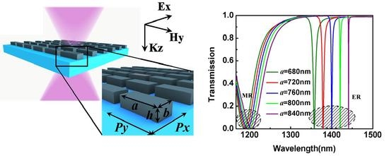
The structure of the all-dielectric metasurface is shown in Figure 1a, where a silicon rectangular rod array (n = 3.45) is deposited on top of a semi-infinite quartz substrate (n = 1.46). And it can be easily fabricated by plasma-enhanced chemical vapor deposition (PECVD), electron-beam lithography, residual resist etching and lift-off process [6,35]. Unlike most previously reported rod-type all-dielectric metasurfaces, where normal incident light polarized along the rods is used to excite a broad ER [5,6,36,37,39], in this paper, the electric field of the incident wave is polarized perpendicular to the rods (i.e., in x-axis). Numerical simulations are conducted using the commercial CST software (CST Studio Suite 2014, CST company, Darmstadt, Germany) at frequency-domain, and periodic boundary conditions are utilized both in x and y directions and open boundary condition are used in the wave propagating direction of z. The lattice periods in the x and y direction are fixed as Px = 800 nm and Py = 900 nm, respectively.
Figure 1b shows the simulated transmission spectrum. Two strong and clear dips are observed in the wavelength range of 1100 nm to 1400 nm. To interpret the origin of these two resonance dips, the field distribution inside the silicon rod are calculated and illustrated in Figure 2. For the broad resonance at shorter wavelength of 1187 nm, the electric and magnetic field are illustrated in Figure 2a,b. The electric and magnetic fields are mainly localized inside the dielectric rods, and the electric field in the x-z plane is greatly enhanced (Figure 2a) showing a typical loop surrounding the rod. However, due to the existence of the quartz substrate, the electric field distribution is not uniform and exhibits strong directional emission into the substrate. Meanwhile, the azimuthal component of the displacement current inside each rod results that the magnetic field linearly polarizes along y direction in the center of the rod in the x-y plane at the same wavelength (Figure 2b). It mainly corresponds to MR and a typical fundamental mode of the dielectric rod resonator [40]. While for the narrow resonance at longer wavelength of 1357 nm, the strong electric field (Figure 2c) is polarized in the central region of the rod along x direction and formed ring-type at both side of dielectric rod. According to the Maxwell electromagnetic theory, a strong magnetic field (Figure 2d) at the cross-section (y-z plane) is induced along the azimuth by the large displacement current, which corresponds to ER and a typical high order mode of the rod resonator [40], though it is usually hybridized due to the coupling between neighboring rods [41].
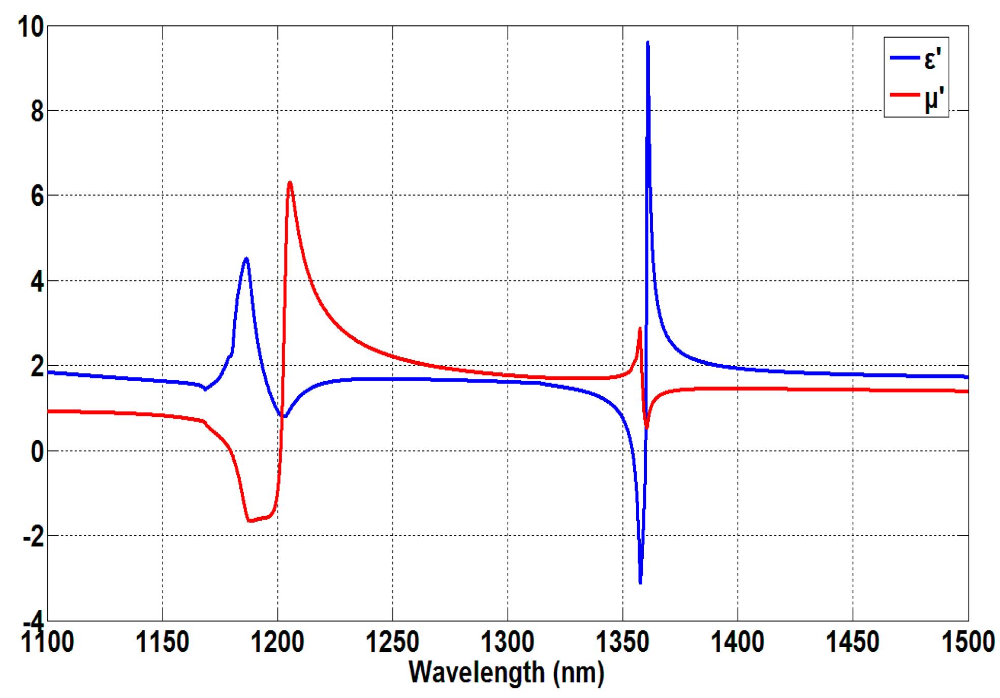
As Yang et al. [39] indicated that both ER and MR contributed to the resonance in a long rod silicon metasurface when a normal incident light is polarized along the rods, to further confirm the distinct ER and MR behavior, we also adopted a standard S-parameter retrieval method [42] to compute the effective permittivity and permeability shown in Figure 3. At the resonance wavelength of ~1187 nm, it shows negative permeability and positive permittivity which explain that this resonance is mainly attributed to the MR, but affected by the coupling between the MR and the ER. Whereas the ER dominates the resonance at the wavelength at 1360 nm in spite of very small coupling of the ER to the MR response.
In order to further study the resonance properties, the wavelength dependences of ER and MR on the geometric parameters (the length and the width) of dielectric rod are calculated in Figure 4. Both the ER and MR resonances show red-shift as the rod’s length or width increases. Linear fits of the dip wavelength versus the geometric parameters are shown in Figure 4b,d, which confirm that the wavelength of the ER is sensitive to both the rod’s length and width, whereas the wavelength of the MR is more sensitive to the rod’s width, which is mainly due to the displacement current loop covers a larger area in the x-z plane for larger value of the rod’s width. And the spectral width of the MR is wide (low Q ~10) and insensitive to the rod parameters due to its fundamental mode of the rods and easy excitation property, however, it is interestingly found that this is just opposite for the ER, i.e., the Q-factor of the ER is not only very high, but also very sensitive to the rod parameters. The Q-factor of the sharp ER with respect to the rod’s length a is calculated and shown in Figure 5 when the rod’s widths are b = 300 nm and b = 260 nm, while the height is fixed at h = 200 nm. As the rod length increases from 680 nm to 800 nm, the Q value of the ER increases steadily, then a dramatic rise is observed and reaches 4500 when a = 840 nm, b = 260 nm. By further increasing the rod’s length, the Q value of over tens of thousands can be expected. However, this kind of growth is not unlimited, since the ER will vanish when the length of the rectangular rod resonators is too close to the period of Py = 900 nm. Not to mention it is expensive or even impossible to fabricate the proposed metasurface when a > 840 nm. Simulation results also indicate that the Q value of the ER increases as the rod width or height decreases. For example, it reaches 25,300 when a = 840 nm, b = 230 nm, h = 200 nm, and further decreasing the rod width or height will result in disappearance of the ER. Based on our simulations, we can conclude that different from a single silicon rod resonator, there exists a critical condition or boundary of the rod’s geometric parameters for the excitation of high order in rod arrays, and less coupling efficiency of the incident light to this resonator mode or higher Q resonance can be obtained near the boundary. And the rod’s length contributes much more to the high Q ER resonance than the rod’s width or height. Although high order ER or MR resonances have been reported [6,41], strong resonance with high Q over several hundreds has not yet been calculated in silicon metasurfaces without asymmetrical structure. Fortunately, the wavelength of the ER discussed above is beyond the diffraction of periodically arranged rod arrays, while this is not the case for the MR with limited applications [43]. Moreover, we should mention here that in the case of oblique incidences, when the angle of incidence plane wave is less than 10 degrees, the Q-factor of the ER will not be changed according to our simulations.
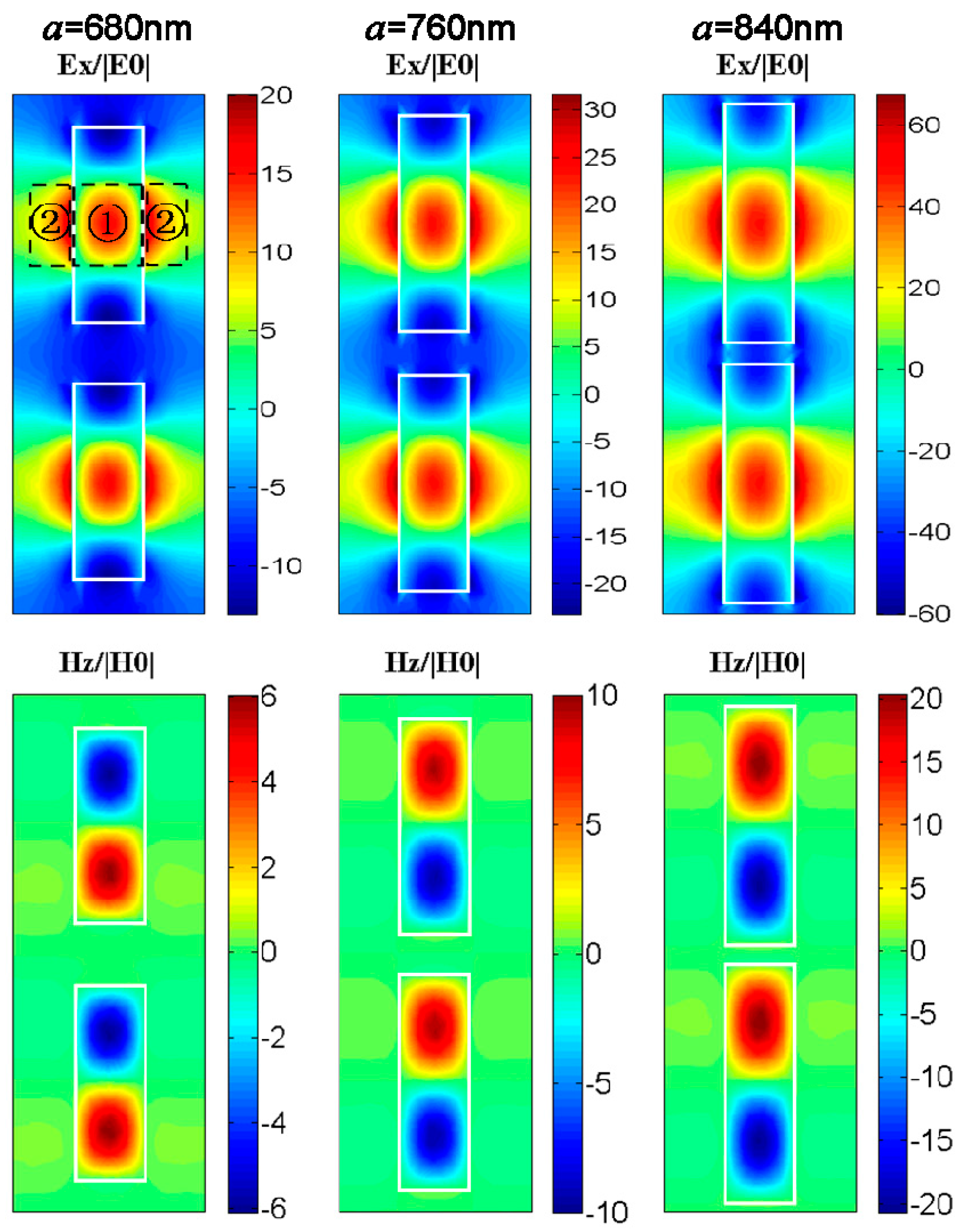
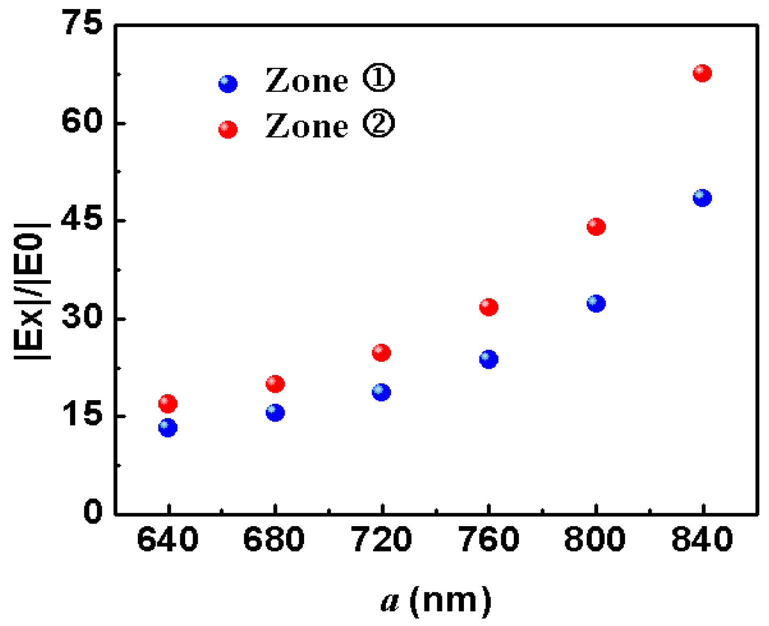
High Q resonance is usually accompanied with the near field enhancement which is useful for nonlinear interactions [7,38] or sensing applications [5,6,36,37]. As the Q value of the ER is more sensitive to the rod’s length, the electric and magnetic field enhancement at the wavelength of the ER and the coupling of adjacent rods in the y-direction with respect to the rod’s length are calculated and shown in Figure 6. It is clearly to see the typical resonator mode inside the rectangular rods and mode hybridization in the surrounding rods. And the magnetic field is well confined inside the rods, while the electric energy is mainly distributed both inside and surrounding the rods. When the rod’s length increases from 680 nm to 840 nm, the electric field enhancement factors both inside the rods (zone ① in Figure 6) and surrounding the rods (zone ② in Figure 6) increases exponentially as shown in Figure 7. The field enhancement factors in zone ① and ② can reach 48.5 and 67.5, respectively, which are comparable to plasmonic nanostructures [36]. Moreover, as the rod length increases, the gap between adjacent rods in the y-direction decreases, the local field coupling between the adjacent rods becomes stronger, leading to the depression of resonance radiation into free space, hence the Q value of the resonance is improved. However, due to the weak mode coupling between the neighboring rods in the x-direction, the decrease of the distance will not improve the resonance Q.
3. Conclusions
In summary, sharp electric resonance with extremely high Q-factor over several thousands are achieved in a simple all-dielectric silicon rod arrays without asymmetric structure. In the mean time, large electric field enhancement both inside and surrounding the rods is observed. A plane wave with its electric field polarized perpendicular to the rod (instead of parallel) illuminates on the metasurface, hence strong high order ER () with high Q value is excited. The electric field coupling between adjacent rods is enhanced by increasing the length of the rod, thus the radiation loss of the ER is significantly depressed, which further explains the source of the high Q value. The resonant wavelength, the Q value and the field enhancement factors versus various geometrical parameters are calculated. The proposed all-dielectric metasurface has many advantages, such as low loss, simple structure, and CMOS-compatible. This structure can be widely used in applications, such as label-free bio-chemical sensing, narrowband filters, optical modulations and nonlinear interactions.
Acknowledgements
This work was supported by the National Natural Science Foundation of China under Grant Nos. 61377108, 61405182.
Author Contributions
Chuanshuai Sui designed the structure and performed the numerical simulations; Xiangjun Li, Tingting Lang, Xufeng Jing and Jianjun Liu analyzed the simulations and modified the article; Zhi Hong putted forward the idea, analyzed the date and wrote the article.
Conflicts of Interest
The authors declare no conflict of interest.
References
- Meinzer, N.; Barnes, W.L.; Hooper, I.R. Plasmonic meta-atoms and metasurfaces. Nat. Photonics 2014, 8, 889–898. [Google Scholar] [CrossRef] [Green Version]
- Gu, J.; Singh, R.; Liu, X.; Zhang, X.; Ma, Y.; Zhang, S.; Maier, S.A.; Tian, Z.; Azad, A.K.; Chen, H.L.; et al. Active control of electromagnetically induced transparency analogue in terahertz metamaterials. Nat. Commun. 2012, 3, 1151. [Google Scholar] [CrossRef] [PubMed]
- Singh, R.; Cao, W.; Al-Naib, I.; Cong, L.; Withayachumnankul, W.; Zhang, W. Ultrasensitive terahertz sensing with high-Q Fano resonances in metasurfaces. Appl. Phys. Lett. 2014, 105, 41–48. [Google Scholar] [CrossRef]
- Jahani, S.; Jacob, Z. All-dielectric metasurfaces. Nat. Nanotechnol. 2016, 11, 23–26. [Google Scholar] [CrossRef] [PubMed]
- Wu, C.; Arju, N.; Kelp, G. Spectrally selective chiral silicon metasurfaces based on infrared Fano resonance. Nat. Commun. 2014, 5, 3892. [Google Scholar] [CrossRef] [PubMed]
- Yang, Y.; Kravchenko, I.I.; Briggs, D.P. All-dielectric metasurface analogue of electromagnetically induced transparency. Nat. Commun. 2014, 5, 5753. [Google Scholar] [CrossRef] [PubMed]
- Li, G.; Zhang, S.; Zentgraf, T. Nonlinear photonic metasurfaces. Nat. Rev. Mater. 2017, 2, 17010. [Google Scholar] [CrossRef]
- Boltasseva, A.; Atwater, H.A. Low-loss plasmonic metamaterials. Science 2011, 331, 290–291. [Google Scholar] [CrossRef] [PubMed]
- Fedotov, V.A.; Rose, M.; Prosvirnin, S.L.; Papasimakis, N.; Zheludev, N.I. Sharp trapped-mode resonances in planar metamaterials with a broken structural symmetry. Phys. Rev. Lett. 2007, 99, 147401. [Google Scholar] [CrossRef] [PubMed]
- Cao, W.; Singh, R.; Al-Naib, I.; He, M.; Taylor, A.J.; Zhang, W. Low-loss ultra-high-Q dark mode plasmonic Fano metamaterials. Opt. Lett. 2012, 37, 3366–3368. [Google Scholar] [CrossRef] [PubMed]
- Al-Naib, I.; Jansen, C.; Singh, R.; Walther, M.; Koch, M. Novel THz metamaterial designs: From near-and far-field coupling to high-Q resonances. IEEE Trans. Terahertz Sci. Technol. 2013, 3, 772–782. [Google Scholar] [CrossRef]
- Al-Naib, I.; Hebestreit, E.; Rockstuhl, C.; Lederer, F.; Christodoulides, D.; Ozaki, T.; Morandotti, R. Conductive coupling of split ring resonators: A path to THz metamaterials with ultrasharp resonances. Phys. Rev. Lett. 2014, 112, 183903. [Google Scholar] [CrossRef] [PubMed]
- Luk’yanchuk, B.; Zheludev, N.I.; Maier, S.A.; Halas, N.J.; Nordlander, P.; Giessen, H.; Chong, C.T. The Fano resonance in plasmonic nanostructures and metamaterials. Nat. Mater. 2010, 9, 707–715. [Google Scholar] [CrossRef] [PubMed]
- Srivastava, Y.K.; Cong, L.; Singh, R. Dual-surface flexible THz Fano metasensor. Appl. Phys. Lett. 2017, 111, 201101. [Google Scholar] [CrossRef]
- Dayal, G.; Solanki, A.; Chin, X.Y.; Sum, T.C.; Soci, C.; Singh, R. High-Q plasmonic infrared absorber for sensing of molecular resonances in hybrid lead halide perovskites. J. Appl. Phys. 2017, 122, 73101. [Google Scholar] [CrossRef]
- Gupta, M.; Singh, R. Toroidal versus Fano resonances in high Q planar THz metamaterials. Adv. Opt. Mater. 2016, 4, 2119–2125. [Google Scholar] [CrossRef]
- Srivastava, Y.K.; Manjappa, M.; Krishnamoorthy, H.N.S.; Singh, R. Accessing the high-Q dark plasmonic Fano resonances in superconductor metasurfaces. Adv. Opt. Mater. 2016, 4, 1875–1881. [Google Scholar] [CrossRef]
- Dayal, G.; Chin, X.Y.; Soci, C.; Singh, R. High-Q Whispering-Gallery-Mode-Based Plasmonic Fano Resonances in Coupled Metallic Metasurfaces at Near Infrared Frequencies. Adv. Opt. Mater. 2016, 4, 1295–1301. [Google Scholar] [CrossRef]
- Staude, I.; Schilling, J. Metamaterial-inspired silicon nanophotonics. Nat. Photonics 2017, 11, 274–284. [Google Scholar] [CrossRef]
- Zhao, Q.; Zhou, J.; Zhang, F.; Lippens, D. Mie resonance-based dielectric metamaterials. Mater. Today 2009, 12, 60–69. [Google Scholar] [CrossRef]
- Ahmadi, A.; Mosallaei, H. Physical configuration and performance modeling of all-dielectric metamaterials. Phys. Rev. B 2008, 77, 45104. [Google Scholar] [CrossRef]
- Schuller, J.A.; Zia, R.; Taubner, T.; Brongersma, M.L. Dielectric metamaterials based on electric and magnetic resonances of silicon carbide particles. Phys. Rev. Lett. 2007, 99, 107401. [Google Scholar] [CrossRef] [PubMed]
- Popa, B.; Cummer, S.A. Compact dielectric particles as a building block for low-loss magnetic metamaterials. Phys. Rev. Lett. 2008, 100, 207401. [Google Scholar] [CrossRef] [PubMed]
- Headland, D.; Nirantar, S.; Withayachumnankul, W.; Gutruf, P.; Abbott, D.; Bhaskaran, M.; Fumeaux, C.; Sriram, S. Terahertz magnetic mirror realized with dielectric resonator antennas. Adv. Mater. 2015, 27, 7137–7144. [Google Scholar] [CrossRef] [PubMed]
- Ginn, J.C.; Brener, I.; Peters, D.W.; Wendt, J.R.; Stevens, J.O.; Hines, P.F. Realizing optical magnetism from dielectric metamaterials. Phys. Rev. Lett. 2012, 108, 97402. [Google Scholar] [CrossRef] [PubMed]
- Kuznetsov, A.I.; Miroshnichenko, A.E.; Fu, Y.H.; Zhang, J.; Luk’Yanchuk, B. Magnetic light. Sci. Rep. 2012, 2, 492. [Google Scholar] [CrossRef] [PubMed]
- Němec, H.; Kužel, P.; Kadlec, F.; Kadlec, C.; Yahiaoui, R.; Mounaix, P. Tunable terahertz metamaterials with negative permeability. Phys. Rev. B 2009, 79, 241108. [Google Scholar] [CrossRef]
- Yahiaoui, R.; Němec, H.; Kužel, P.; Kadlec, F.; Kadlec, C.; Mounaix, P. Broadband dielectric terahertz metamaterials with negative permeability. Opt. Lett. 2009, 34, 3541–3543. [Google Scholar] [CrossRef] [PubMed]
- Yahiaoui, R.; Chung, U.-C.; Elissalde, C.; Maglione, M.; Vigneras, V.; Mounaix, P. Towards left-handed metamaterials using single-size dielectric resonators: The case of TiO2-disks at millimeter wavelengths. Appl. Phys. Lett. 2012, 101, 42909. [Google Scholar] [CrossRef]
- Yahiaoui, R.; Němec, H.; Kužel, P.; Kadlec, F.; Kadlec, C.; Mounaix, P. Tunable THz metamaterials based on an array of paraelectric SrTiO3 rods. Appl. Phys. A 2011, 103, 689–692. [Google Scholar] [CrossRef]
- Yahiaoui, R.; Chung, U.-C.; Burokur, S.N.; de Lustrac, A.; Ellssalde, C.; Maglione, M.; Vigneras, V.; Mounaix, P. Broadband effective magnetic response of inorganic dielectric resonator-based metamaterial for microwave applications. Appl. Phys. A 2014, 114, 997–1002. [Google Scholar] [CrossRef] [Green Version]
- Kuznetsov, A.I.; Miroshnichenko, A.E.; Brongersma, M.L.; Kivshar, Y.S.; Luck’yanchuk, B. Optically resonant dielectric nanostructures. Science 2016, 354, 2472. [Google Scholar] [CrossRef] [PubMed]
- Arbabi, A.; Horie, Y.; Bagheri, M.; Faraon, A. Dielectric metasurfaces for complete control of phase and polarization with subwavelength spatial resolution and high transmission. Nat. Nanotechnol. 2015, 10, 937–943. [Google Scholar] [CrossRef] [PubMed]
- Arbabi, A.; Arbabi, E.; Horie, Y.; Kamali, S.M.; Faraon, A. Planar metasurface retroreflector. Nat. Photonics 2017, 11, 415–420. [Google Scholar] [CrossRef]
- Campione, S.; Liu, S.; Basilio, L.I.; Warne, L.K.; Langston, W.L. Broken symmetry dielectric resonators for high quality factor Fano metasurfaces. ACS Photonics 2016, 3, 2362–2367. [Google Scholar] [CrossRef]
- Zhang, J.; Liu, W.; Zhu, Z.; Yuan, X.; Qin, S. Strong field enhancement and light-matter interactions with all-dielectric metamaterials based on split bar resonators. Opt. Express 2014, 22, 30889–30898. [Google Scholar] [CrossRef] [PubMed]
- Zhang, J.; MacDonald, K.F.; Zheludev, N.I. Near-infrared trapped mode magnetic resonance in an all-dielectric metamaterial. Opt. Express 2013, 21, 26721–26728. [Google Scholar] [CrossRef] [PubMed]
- Yang, Y.; Wang, W.; Boulesbaa, A.; Kravchenko, I.I.; Briggs, D.P.; Puretzky, A.; Geohegan, D.; Valentine, J. Nonlinear Fano-resonant dielectric metasurfaces. Nano Lett. 2015, 15, 7388–7393. [Google Scholar] [CrossRef] [PubMed]
- Yang, Y.; Miroshnichenko, A.E.; Kostinski, S.V.; Odit, M.; Kapitanova, P.; Qiu, M.; Kivshar, Y. Multimode directionality in all-dielectric metasurfaces. Phys. Rev. B 2017, 95, 165426. [Google Scholar] [CrossRef]
- Wang, J.; Xu, Z.; Yu, Z.; Wei, X.; Yang, Y.; Wang, J.; Qu, S. Experimental realization of all-dielectric composite cubes/rods left-handed metamaterial. J. Appl. Phys. 2011, 109, 84918. [Google Scholar] [CrossRef]
- Zywietz, U.; Schmidt, M.K.; Evlyukhin, A.B.; Reinhardt, C.; Aizpurua, J.; Chichkov, B.N. Electromagnetic resonances of silicon nanoparticle dimers in the visible. ACS Photonics 2015, 2, 913–920. [Google Scholar] [CrossRef]
- Smith, D.R.; Vier, D.C.; Koschny, T.; Soukoulis, C.M. Electromagnetic parameter retrieval from inhomogeneous metamaterials. Phys. Rev. E 2005, 71, 36617. [Google Scholar] [CrossRef] [PubMed]
- Sui, C.; Han, B.; Lang, T.; Li, X.; Jing, X.; Hong, Z. Electromagnetically induced transparency in an all-dielectric metamaterial-waveguide with large group index. IEEE Photonics J. 2017, 9, 4600708. [Google Scholar] [CrossRef]
Figure 1.
(a) Schematic diagram of the unit cell for the all-dielectric metasurface. The length, width and height of the silicon rod are represented by a, b, and h. The lattice constants of unit cell are Px (800 nm) × Py (900 nm); (b) Transmission of the silicon rod arrays for the geometrical parameters of a = 680 nm, b = 300 nm, h = 200 nm. ER: electrical resonance; MR: magnetic response.

Figure 2.
Field distribution inside one unit cell of the rod array. (a,b) |E| in x-z plane and |H| in x-y plane at wavelength of 1187 nm, representing the magnetic dipole moment; (c,d) |E| in x-z plane and |H| in x-y plane at wavelength of 1357 nm, representing the higher order electric dipole moment.
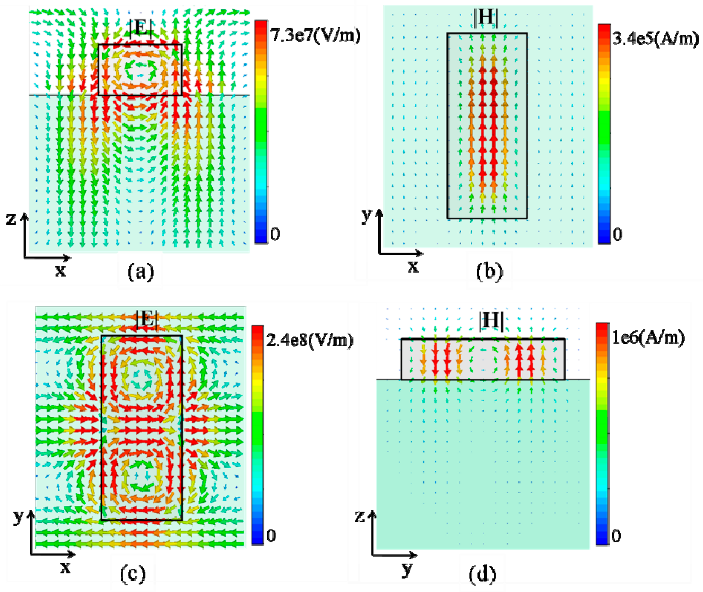
Figure 3.
The real parts of effective permittivity (ε′) and permeability (μ′).

Figure 4.
(a,c): Transmission spectra of the metasurface as a function of the rod’s length a (b = 300 nm) and width b (a = 800 nm), respectively. (b,d): The wavelength dependence of electrical resonance (ER) and magnetic response (MR) on the rod’s length a and width b, respectively. The rod’s height is fixed at 200 nm.
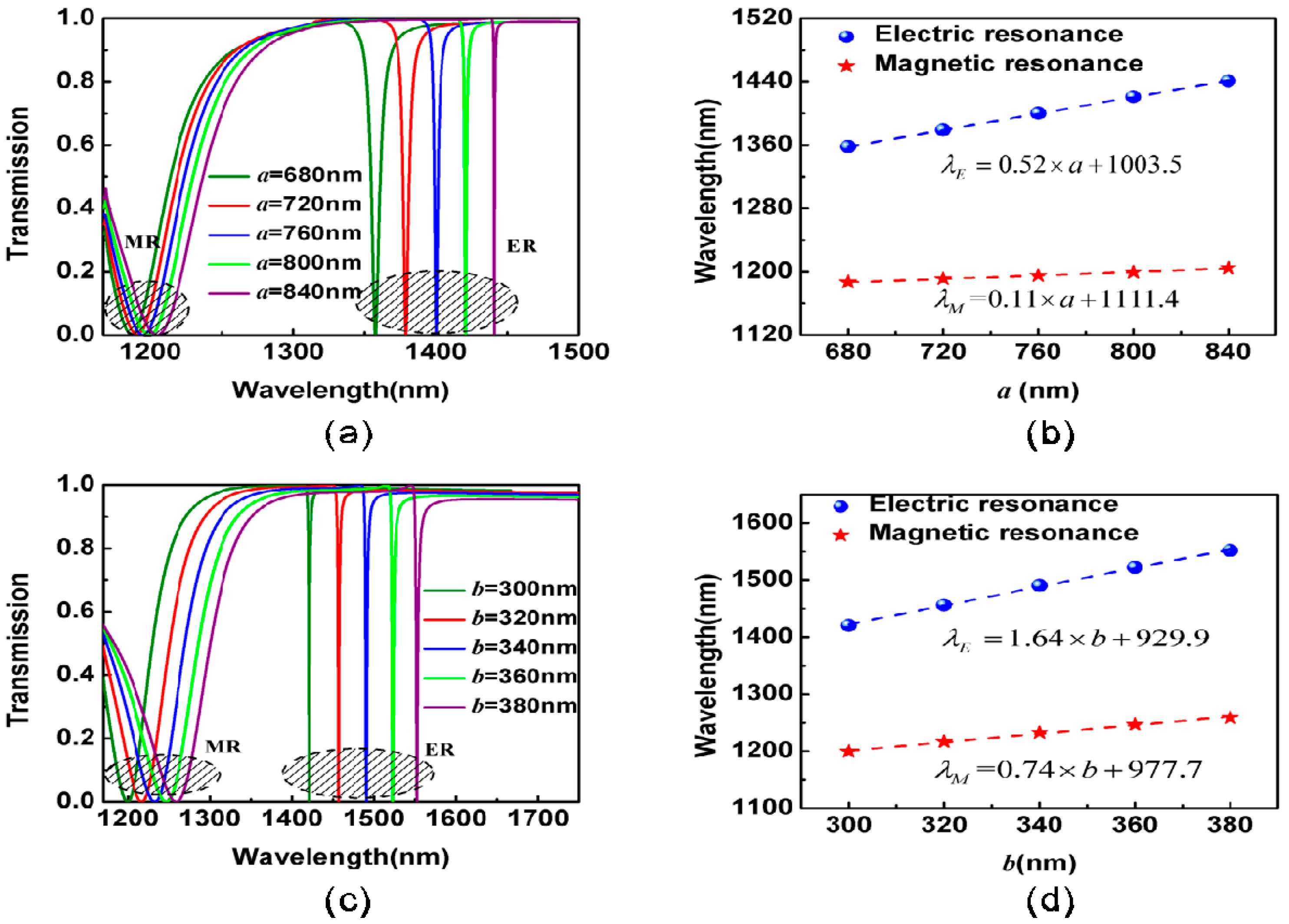
Figure 5.
Calculated Q-factors of ER as a function of the rod’s length a for b = 260 nm and 300 nm when h = 200 nm.
Figure 5.
Calculated Q-factors of ER as a function of the rod’s length a for b = 260 nm and 300 nm when h = 200 nm.
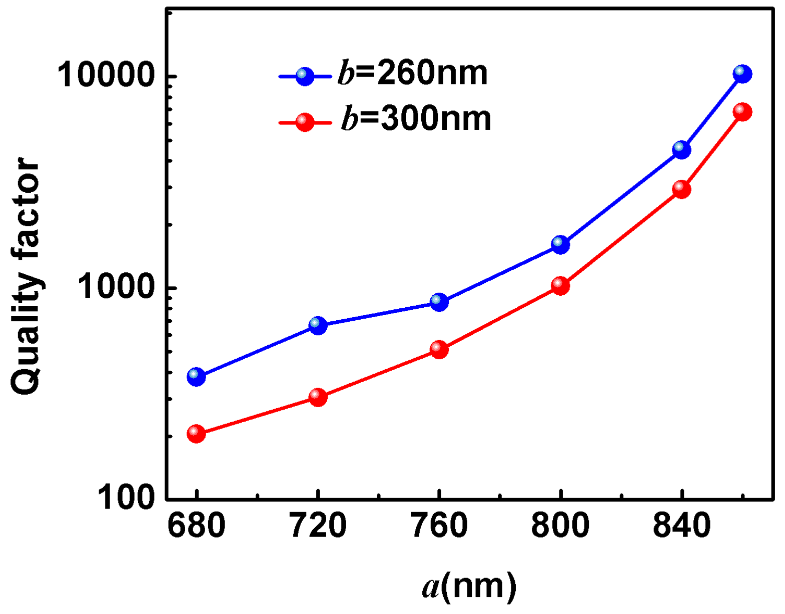
Figure 6.
Simulated electric (Ex) and magnetic field (Hz) at ER (normalized to the incident field amplitude E0 and H0) at the x-y plane bisecting the nanobars when rod length a = 680 nm, 760 nm, and 840 nm.
Figure 6.
Simulated electric (Ex) and magnetic field (Hz) at ER (normalized to the incident field amplitude E0 and H0) at the x-y plane bisecting the nanobars when rod length a = 680 nm, 760 nm, and 840 nm.

Figure 7.
Dependence of the field enhancement factor (|Ex|/|E0|) on the rod’s length at zone ① and ②.
Figure 7.
Dependence of the field enhancement factor (|Ex|/|E0|) on the rod’s length at zone ① and ②.
© 2018 by the authors. Licensee MDPI, Basel, Switzerland. This article is an open access article distributed under the terms and conditions of the Creative Commons Attribution (CC BY) license (http://creativecommons.org/licenses/by/4.0/).
Share and Cite
MDPI and ACS Style
Sui, C.; Li, X.; Lang, T.; Jing, X.; Liu, J.; Hong, Z. High Q-Factor Resonance in a Symmetric Array of All-Dielectric Bars. Appl. Sci. 2018, 8, 161. https://doi.org/10.3390/app8020161
AMA Style
Sui C, Li X, Lang T, Jing X, Liu J, Hong Z. High Q-Factor Resonance in a Symmetric Array of All-Dielectric Bars. Applied Sciences. 2018; 8(2):161. https://doi.org/10.3390/app8020161
Chicago/Turabian StyleSui, Chuanshuai, Xiangjun Li, Tingting Lang, Xufeng Jing, Jianjun Liu, and Zhi Hong. 2018. "High Q-Factor Resonance in a Symmetric Array of All-Dielectric Bars" Applied Sciences 8, no. 2: 161. https://doi.org/10.3390/app8020161
Note that from the first issue of 2016, this journal uses article numbers instead of page numbers. See further details here.