Theoretical Study of a 0.22 THz Backward Wave Oscillator Based on a Dual-Gridded, Carbon-Nanotube Cold Cathode


1
School of Electronic Science and Engineering, University of Electronic Science and Technology of China, Chengdu 610054, China
2
Department of Electronic and Electrical Engineering, University of Bath, North Road BA2 7AY, UK
3
State Key Laboratory Optoelectronic Materials and Technologies, Sun Yat-sen University, Guangzhou 510275, China
*
Author to whom correspondence should be addressed.
Appl. Sci. 2018, 8(12), 2462; https://doi.org/10.3390/app8122462
Submission received: 25 October 2018
/
Revised: 28 November 2018
/
Accepted: 29 November 2018
/
Published: 2 December 2018
(This article belongs to the Section Nanotechnology and Applied Nanosciences)
Abstract
:The carbon nanotube (CNT) cold cathode is an attractive choice for millimeter and terahertz vacuum electronic devices owning to its unique instant switch-on and high emission current density. A novel, dual-gridded, field emission architecture based on a CNT cold cathode is proposed here. CNTs are synthesized directly on the cathode surface. The first separating grid is attached to the CNT cathode surface to shape the CNT cathode array. The second separating grid is responsible for controlled extraction of electrons from the CNT emitters. The cathode surface electric field distribution has been improved drastically compared to conventional planar devices. Furthermore, a high-compression-ratio, dual-gridded, CNT-based electron gun has been designed to further increase the current density, and a 21 kV/50 mA electron beam has been obtained with beam transparency of nearly 100%, along with a compression ratio of 39. A 0.22 THz disk-loaded waveguide backward wave oscillator (BWO) based on this electron gun architecture has been realized theoretically with output power of 32 W. The results indicate that higher output power and higher frequency terahertz BWOs can be made using advanced, nanomaterial-based cold cathodes.
1. Introduction
Terahertz radiation sources have gleaned much attention due to the wide range of potential applications of such devices, such as high data rate communications; the identification of concealed weaponry; remote, high-resolution imaging; and biomedical diagnostics [1,2,3,4,5]. Several existing technologies to generate terahertz waves are currently available, including quantum cascade lasers, solid state electron devices, and optical devices [6,7,8,9]. Unfortunately, they have many intrinsic restrictions such as poor anti-interference performance, deleterious responsiveness to incident radiation, and the need for cryogenic cooling, which is often coupled to challengingly low output power.
Vacuum electronic devices (VEDs) have been applied widely to realize terahertz radiation sources due to their high output power and high operation frequency [10,11]. VEDs include gyrotrons, extended-interaction klystrons (EIKs), traveling wave tubes (TWTs), and backward wave oscillators (BWOs) [12,13,14,15]. In particular, the BWO is an effective solution that is capable of producing relatively high power and stable monochromatic terahertz signals. BWOs can be electronically tuned over a wide frequency range around an arbitrary operating frequency and afford high frequency stability, along with compact designs at relatively inexpensive costs. To date, commercially available modern BWOs employ thermionic cathode electron guns that suffer from the need for large working volumes, high temperature operation, and slow temporal response. Field emission cold cathodes are a leading candidate for the replacement of incumbent thermionic electron sources in terahertz BWOs. Cold cathodes offer low operating temperature, instantaneous response time, facile and inexpensive integration, and the potential for miniaturization. 0.22 THz is an important terahertz frequency of atmospheric window, which is of great value in application. Here, a 0.22 THz BWO based on a cold cathode has been designed. Central to this is the development of field emission cold cathode materials suitable for terahertz BWOs.
Carbon nanotubes (CNT)-based field electron emitters have a high emission current density, as well as impressive chemical and temporal stability [16,17,18,19,20], and are well suited to the miniaturization of terahertz VEDs. Nevertheless, there are still various challenges plaguing CNT cold cathode VEDs. Principally, the emission current density of CNT in a large area is very small. Therefore, it is vital to choose a suitable electron gun architecture that has the ability to simultaneously generate a high beam emission current and high emission current density. Several existing types of CNT-based field emission structures have been developed during the last two decades, including Spindt-type, magnetic injection type and separating gridded type [21,22,23,24]. Spindt-type CNT field emission structures have many difficulties and insurmountable processing challenges, such as regular short circuits between the cathode and grid, high grid losses, and poor emission spatial uniformity. A truncated-cone CNT cold cathode electron gun, based on magnetic injection, has proven a need for superconducting magnetic fields in order to confine or control the electron beam [21,22]. Conversely, the separating grid-type CNT field emission structure can be easily achieved in experiments and can operate at lower magnetic field at the gauss level. Such an operation would make the separating gridded structure widely appealing to a variety of small-scale vacuum microelectronic devices. However, it has been reported that a conventional, single-separating, gridded electron gun with the planar annular CNT cold cathode suffers from low emission current, high gate losses, and grid deformation [23], the latter of which stems from the small effective emission area, electrostatic shielding effect, and drop in electric field beneath the grid center.
In this paper, an emerging topology has been introduced by modifying the conventional single separating gridded field emission structure into a dual-gridded field emission structure. This architecture could be effectively used to solve the problem of the reduction of the electric field beneath the center of grid, thereby achieving a relatively uniform electric field distribution on the cathode surface. Therefore, any electrostatic shielding and edge effects would be greatly reduced. Such advantages make the dual-gridded CNT-based electron gun simultaneously produce a high beam emission current and have high emission current density. Furthermore, the two separating grids are coaxial with each other, which dramatically reduces grid interception and losses, thereby ensuring high beam transparency.
2. Design and Simulation
2.1. Dual-Gridded Field Emission Structure Based on CNT Cold Cathode
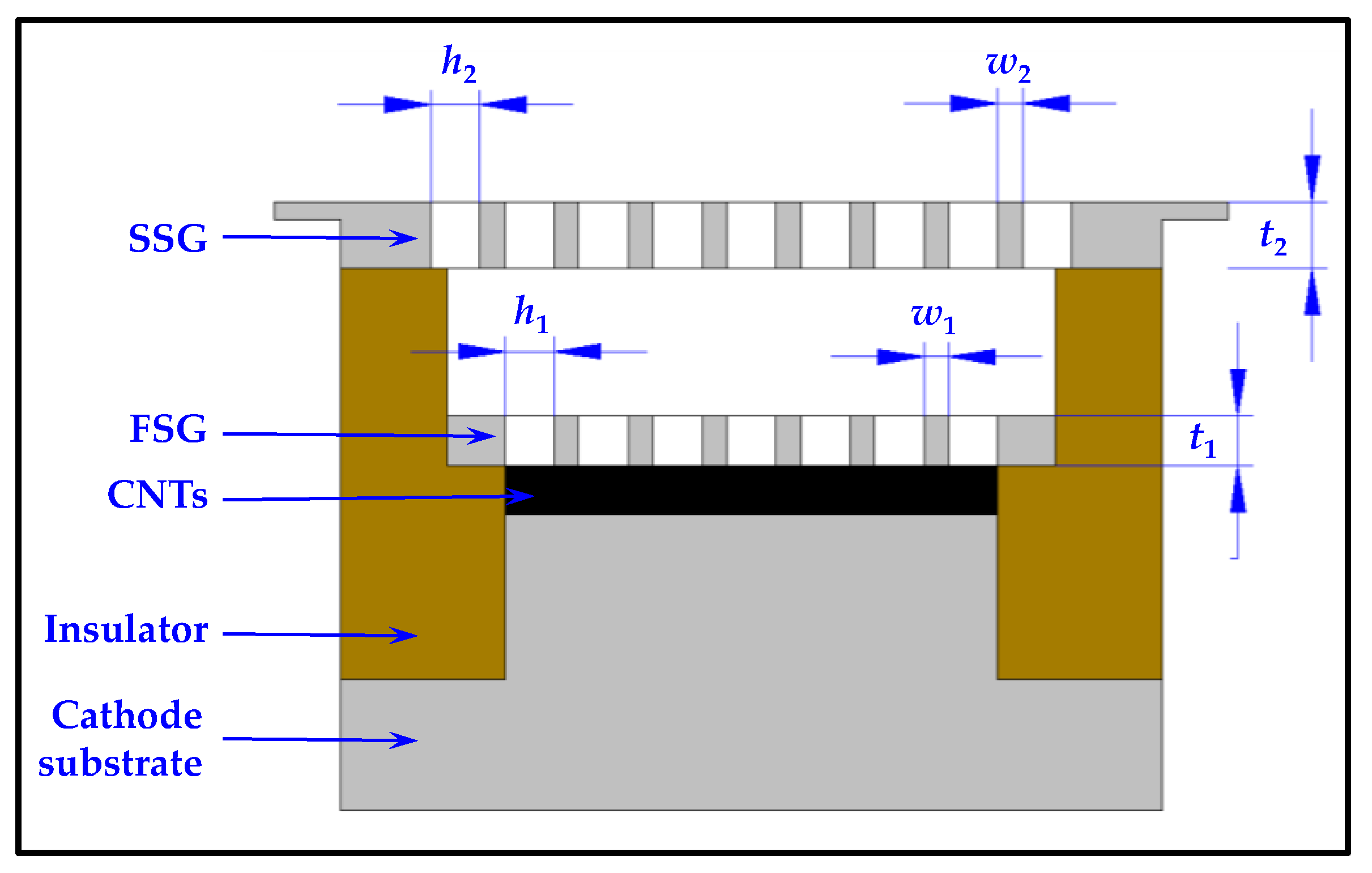
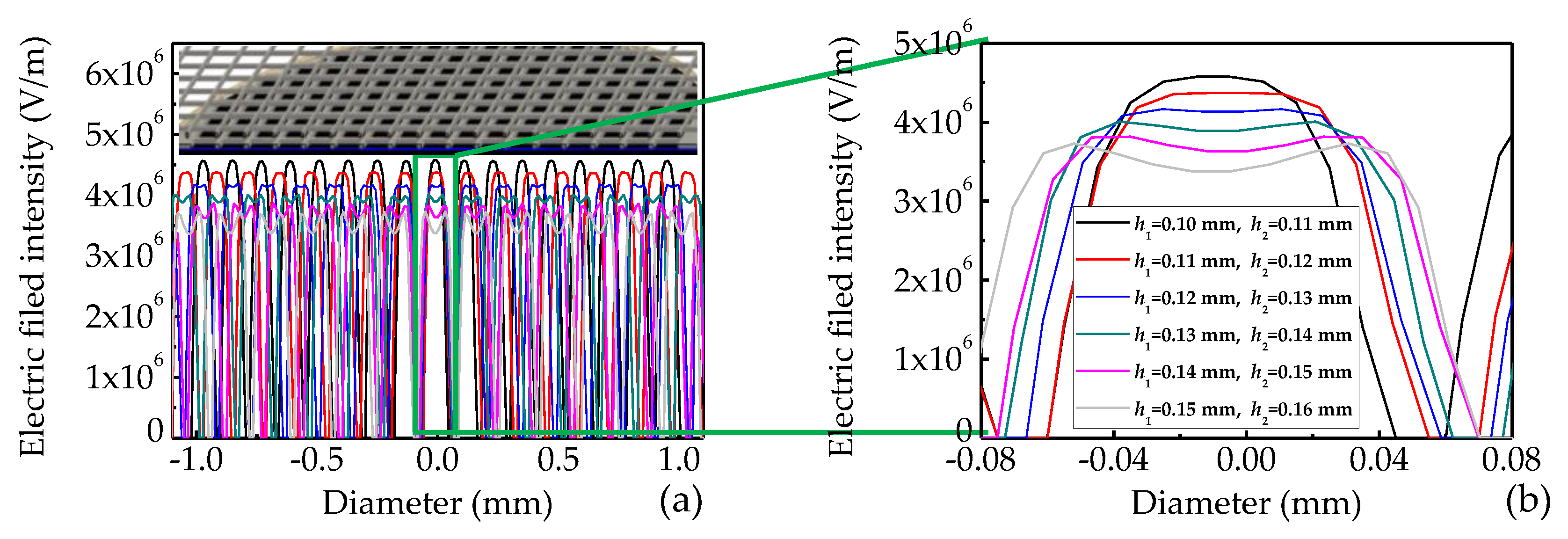
In previous work on conventional gridded triode with planar CNT cold cathodes, non-uniform electric field distributions often appear on the cathode surface [25]. Such devices exhibit large emission current densities immediately beneath the grid, owing to the higher local electric field, with a reduced emission current in the center of grid holes due to the lower effective electric field. This, as a result, allows for greater current interception, and hence losses. Experimental results have shown that low beam transparency may lead to small emission current, high grid losses, arcing, and unwanted grid deformation [23,25]. In response, here we report on the spatial topology of a dual-gridded CNT field emission system. The dual-gridded system is composed of a cathode substrate, a CNT electron emitter, a first separating grid (FSG), a second separating grid (SSG), and an insulator, as depicted in Figure 1. The CNTs are synthesized directly on the cathode substrate surface. The FSG is attached to the cathode surface to mold the cathode array. The SSG is coaxial with the FSG and controls electron extraction from the CNT electron emitters. The two separating grids are connected with each other coaxially through the insulator. The grid mesh holes are square. The design parameters of the specific dual-gridded system are listed in Table 1. The blue line on the surface of the square array (inset Figure 2a) denotes the probed surface under study. The mesh-hole h1 of the FSG is a dominant factor influencing the electric field distribution at the cathode surface in the present optimization. For brevity’s sake, we consider six practically viable h1 values (0.10, 0.11, 0.12, 0.13, 0.14, and 0.15 mm) in the present geometry. Figure 2 shows the electric field distribution along the blue line as function of h1. Correspondingly, the SSG mesh-hole h2 values are 0.11, 0.12, 0.13, 0.14, 0.15, and 0.16 mm, ensuring that the SSG is coaxial with the FSG (h1 + w1 = h2 + w2). It is evident that in this field emission structure the electric field distribution at the effective emission cathode surface is relatively smooth without significant edge effects. The difference in electric field intensity between the maximum and the minimum is less than 0.5 kV/mm, which is <11% variation in the electric field from the center field intensity. The simulation results also illustrate that the surface electric field intensity increases as h1 decreases. However, the smaller h1 causes a rise in the electric field at the center of the square cathode surface, as well as reducing the emission cathode area. The larger unit square cathode area causes a drop in the electric field at the center of the square cathode surface. The rise or drop in electric field at the center of the square cathode surface is, nevertheless, a disadvantage to the production of a uniform emission current. Therefore, an optimal h1 is significant to the current design. Our studies suggest an optimal h1 of 0.12 mm, which is used herein to ensure that the electric field distribution on the emission cathode surface remains relatively uniform (<2.3% variation).
2.2. High-Compression-Ratio CNT Electron Gun Based on Dual-Gridded System
There remain many challenges in the realization of terahertz BWOs based on CNT cold cathodes. Here, a high-compression-ratio CNT electron gun based on the mentioned dual-gridded system above is designed and investigated to overcome many of these limitations. The dual-gridded CNT cold cathode electron gun has been simulated herein using commercially available 3D simulation software (CST). The basic field emission process from such semi-metals is well described by the generalized Fowler-Nordheim equation, in the following form:
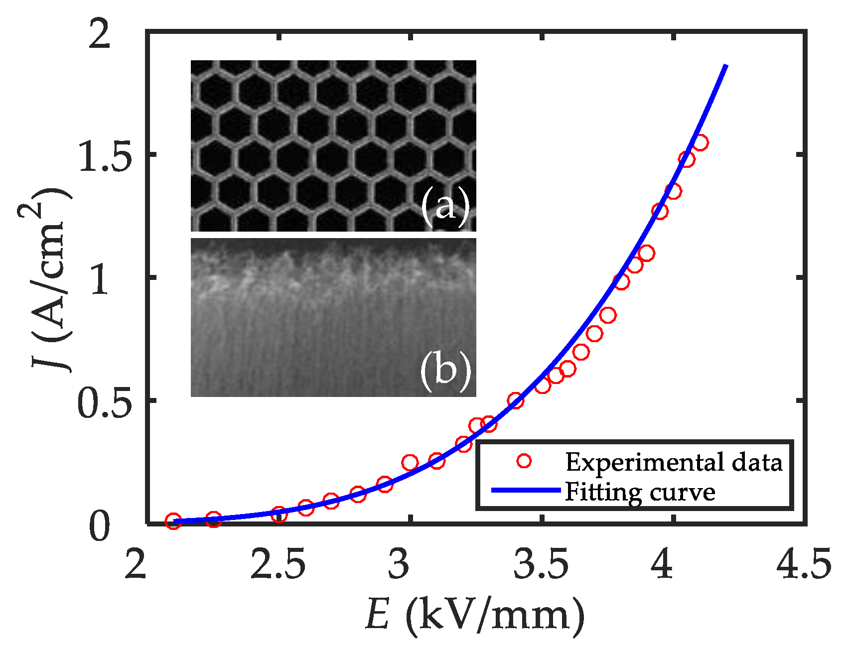
Here, A and B are the approximate Fowler-Nordheim constants, which are estimated by numerical fitting based on the previous experimental results [26]. Applying our fitting procedure (R2 = 0.9897), we find A = 5 × 10⁻⁸ A/V2 and B = 1.62 × 10⁷ V/m. In our previous experimental study [26], we have investigated field emission (FE) of a vertically aligned, well-ordered carbon nanotube (CNT) mesh (VACM) by growing the CNTs in a network with hexagonal holes as shown in the inset (a) of Figure 3. The synthesized carbon nanotubes are uniform, dense, well aligned, and perpendicular to the substrate as shown in the inset (b) of Figure 3. The FE properties of the emitters were determined using a simple diode configuration in a vacuum chamber at a pressure of 1 × 10⁻⁶ Pa. Emission area of 16 mm2 was used. A maximum operating emission current density of 1.5 A/cm2 was obtained at a field of less than 4.5 kV/mm. In this paper, we adopt the VACM as cathode emitters on the smaller substrate surface of 3.91 mm2 at a higher vacuum degree of 1 × 10⁻⁷ Pa. Figure 3 shows typical experimental data and the resulting fitted emission characteristics. It indicates that the dual-gridded electron gun exhibits a maximum emission current of 50 mA at the grid voltage of 0.5 kV (the electric field on the per cathode unit surface is 4.17 kV/mm); the corresponding emission current density J is 1.5 A/cm2 when the effective emission area Se is 3.33 mm2.
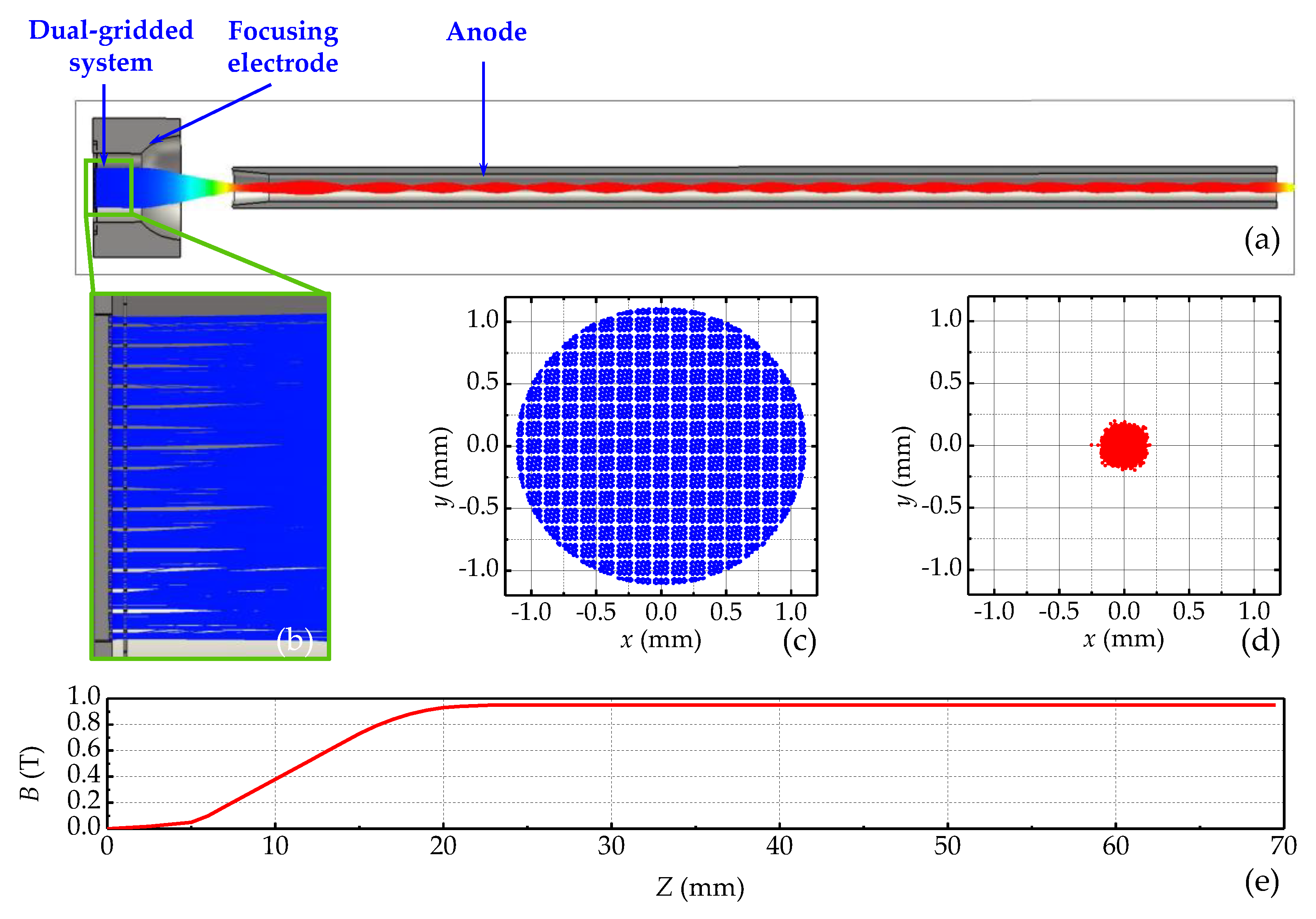
As shown in Figure 4a, the CNT electron gun comprises a dual-gridded system, a focusing electrode, and an anode. The dimensions of dual-gridded system are listed in Table 1. The focusing electrode is connected to the SSG, and the distance between the cathode and anode is 8 mm. In order to obtain a high-compression-ratio electron beam, a suitable axial magnetic field is required. Figure 4a shows the simulated beam trajectories under a field of 0.95 T operating at 21 kV/50 mA. A beam transparency of 100% is obtained, as shown in Figure 4b. Figure 4 e shows the profile of the magnetic field intensity along the central axis. In the cathode region the magnetic field is approximately 0.01 T. At the beam output port, the magnetic field is 0.95 T. Figure 4c,d shows the beam spot cross-section at the cathode surface and anode output port plane of the electron gun. The electron beam cross-section is compressed from the cold cathode emission area of 1.25π mm2 into a beam spot approximately 0.032π mm2 (beam spot radius = 0.18 mm). At the gun exit port, the electron beam cross-sectional area is compressed approximately 39 times, with the beam current density correspondingly enhanced by a comparable amount.
Compared with existing CNT-based cathode electron guns, this kind of dual-gridded electron gun has several advantages. Firstly, the fabrication process of the CNT cathode array is simple and easy to implement. The CNTs film uniformly cover the whole plane substrate surface with high areal density. Then, the dual-gridded system is placed onto the cathode, thereby enabling the FSG to be attached to the cathode surface, and the mesh-holes of the FSG are employed to shape the CNT cathode array. Secondly, an electron beam transparency of 100% can be achieved theoretically, due to the coaxial components of the dual-gridded field emission system. Our findings suggest that the dual-gridded electron gun can successfully avoid grid interception and arcing, and hence offers extended operation life times. As shown in Figure 4a, the electron beam is firstly compressed by the focusing electrode electric field and then is accelerated by the anode prior to entering the beam tunnel. Here, the electron beam undergoes a second compression along the radial direction with the magnetic field gradually increasing with length along the tunnel. The electron beam then passes through the beam tunnel and moves into an interaction cavity.
2.3. A 0.22 THz BWO Based on Dual-Gridded CNT Cold Cathode Electron Gun
Backward wave oscillator (BWO) is one of the most established VED sources of THz radiation. A BWO is a VED that is used to generate microwaves up to the THz frequency range. By adjusting the beam voltage, it tunes fully and rapidly over a very wide band of frequencies [1]. The basic idea of the BWO is to use the electron beam interacting along their path with a periodic slow wave structure (the first space harmonic). When the electron beam passes the periodic structure, it initiates a wave propagating in backward direction. If the total phase delay in the loops is θn = n·2π, a backward wave oscillation can start [27]. When the phase velocity of the normal mode of the SWS equals that of the drifting electrons, each electron feels an accelerating or decelerating force, depending on the local phased of the wave. As a consequence, the beam bunches, but there is no net exchange of energy, because equal numbers of electrons speed up and slow down. If the electrons are initially somewhat faster than the wave, however, more electrons are decelerated than accelerated, and a resonant transfer of energy to the wave occurs in addition to the bunching. In BWO of this type, the exchange of energy causes the wave to grow in amplitude, and the bunching enforces the coherence of the radiation [28].
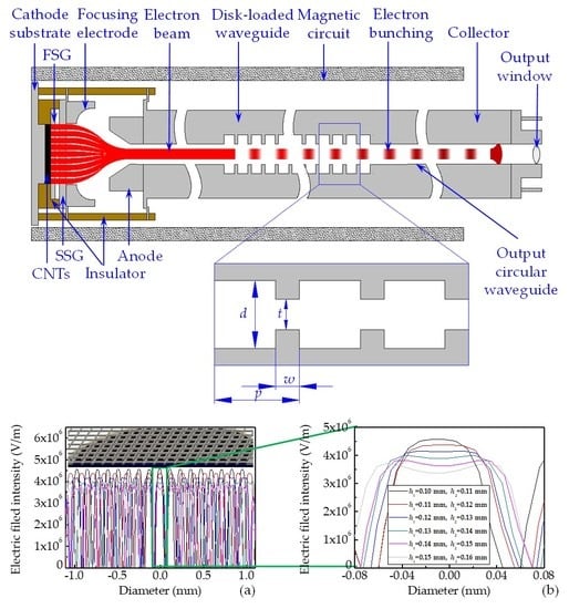
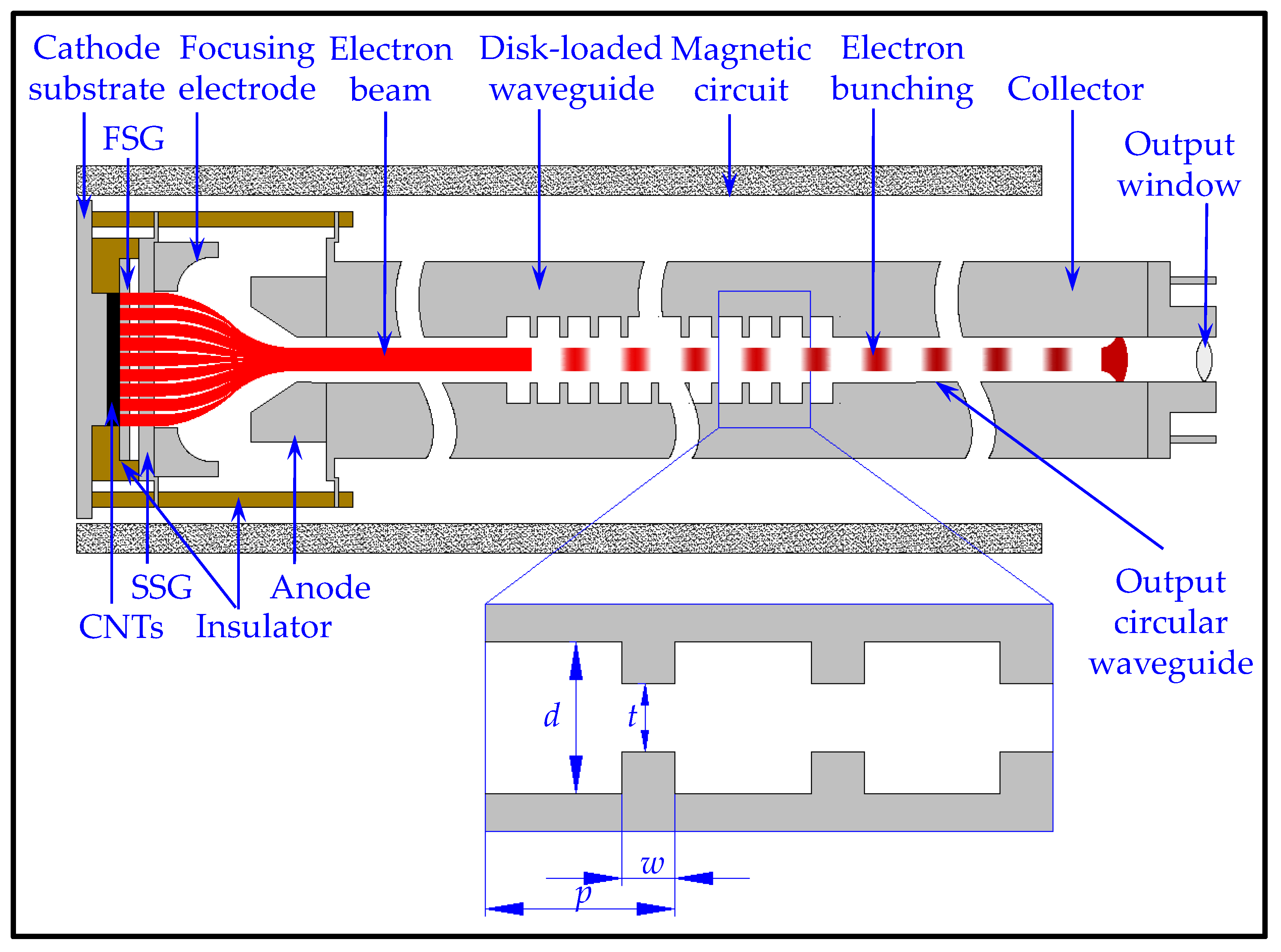
Figure 5 shows the scheme of the inner structure of the proposed CNT terahertz BWO device. The BWO consists of a dual-gridded CNT cold cathode electron gun, a beam-wave interaction slow wave structure (SWS), a collector, an output circular waveguide, an output window, and magnetic circuit. The beam-wave interaction SWS is a disk-loaded waveguide. The operating parameters of the BWO are listed in Table 2.
Firstly, electrons are emitted from the CNT cold cathode under the action of the applied field between the second separating grid and cold cathode. Electrons will be compressed and as a result form an electron beam under the electric and magnetic fields, while they are accelerated by the anode into the beam tunnel. Here, the magnetic field will gradually increase and electric field will not change, resulting in magnetic adiabatic compression of the beam. After the electron beam is compressed in the beam tunnel, it enters the beam-wave interaction SWS, where it initiates and interacts with the TM01 mode thusly generating electromagnetic radiation.
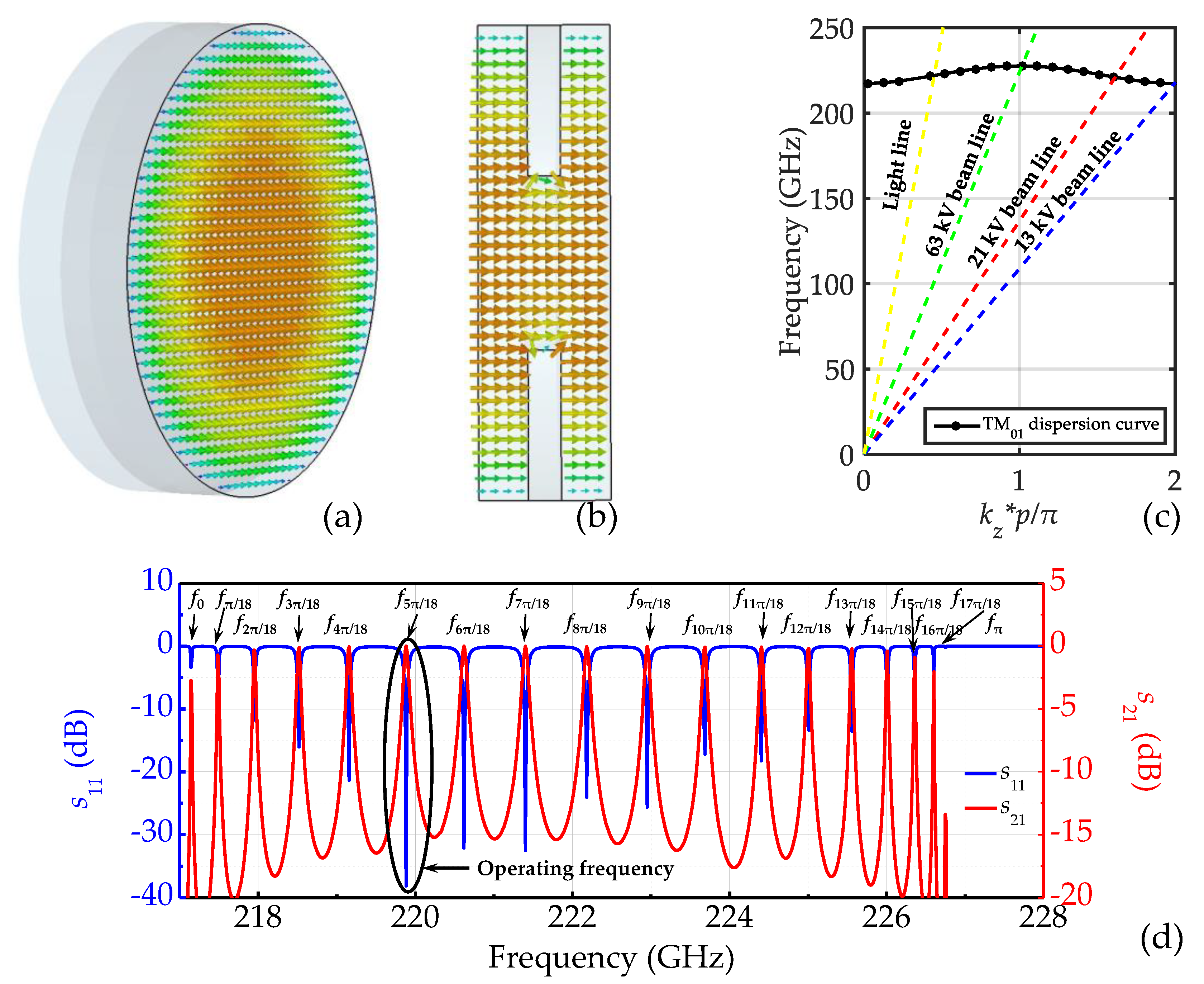
The disk-loaded waveguide structure, as a promising SWS, has attracted wide attention for terahertz VEDs, since it is geometrically suitable to be realized by modern microfabrication processes. The CST eigenmode simulation in Microwave Studio was applied to study the high-frequency characteristics of the disk-loaded waveguide BWO by setting the electric field and periodic boundary to the transverse and longitudinal direction, respectively. Here, the TM01 mode has been selected as an operating mode, as the cylindrical axial electric field Ez of the TM01 mode is concentrated in the center of the SWS, as shown in Figure 6a,b.
The dispersion curve of the TM01 mode is plotted as a function of the normalized wavenumber, as shown in Figure 6c. The 21 kV beam line (dashed red line) is superimposed onto the dispersion curve, intercepting the dispersion curve at an operating frequency of 220 GHz. At the operating frequency, the velocity of the electron beam is synchronous with the phase velocity of the backward wave, which is approximately equal to the slope of the beam line.
A completely symmetric, disk-loaded waveguide SWS structure is modeled to study the reflection and transmission characteristics of the terahertz VED. 20 periods are considered. The S-parameters are calculated by the transient solver in the CST Microwave Studio. Figure 6d shows the magnitudes of the calculated S-parameters. There are 19 resonant frequencies—corresponding to the 0-mode, π/18-mode, 2π/18-mode, 3π/18-mode, 4π/18-mode, 5π/18-mode, 6π/18-mode, 7π/18-mode, 8π/18-mode, 9π/18-mode, 10π/18-mode, 11π/18-mode, 12π/18-mode, 13π/18-mode, 14π/18-mode, 15π/18-mode, 16π/18-mode, 17π/18-mode, and π-mode—observed in both S11 and S12. As per frequency relation formula [29]:
these frequencies correspond to a phase shift “βL” of 0, π/18, 2π/18, 3π/18, 4π/18e, 5π/18, 6π/18, 7π/18, 8π/18, 9π/18, 10π/18, 11π/18, 12π/18, 13π/18, 14π/18, 15π/18, 16π/18, 17π/18, and π, respectively. The frequency passband of the disk-loaded waveguide BWO is largely discrete. As can be seen, S11 remains at about −38 dB around the operating frequency whilst S21 remains at approximately 0 dB, suggesting that the disk-loaded waveguide SWS is indeed well-suited for terahertz BWO applications.
The nonlinear interaction between the electron beam and electromagnetic wave in the disk-loaded waveguide BWO is simulated. Some typical parameters, including output power and operating frequency, are obtained. To make the BWO more practical, a simple matched output circular waveguide is designed, as shown in Figure 5. Unlike the traveling-wave tube (TWT), the BWO does not require an input signal. The output signal is produced by the electron beam during transit.
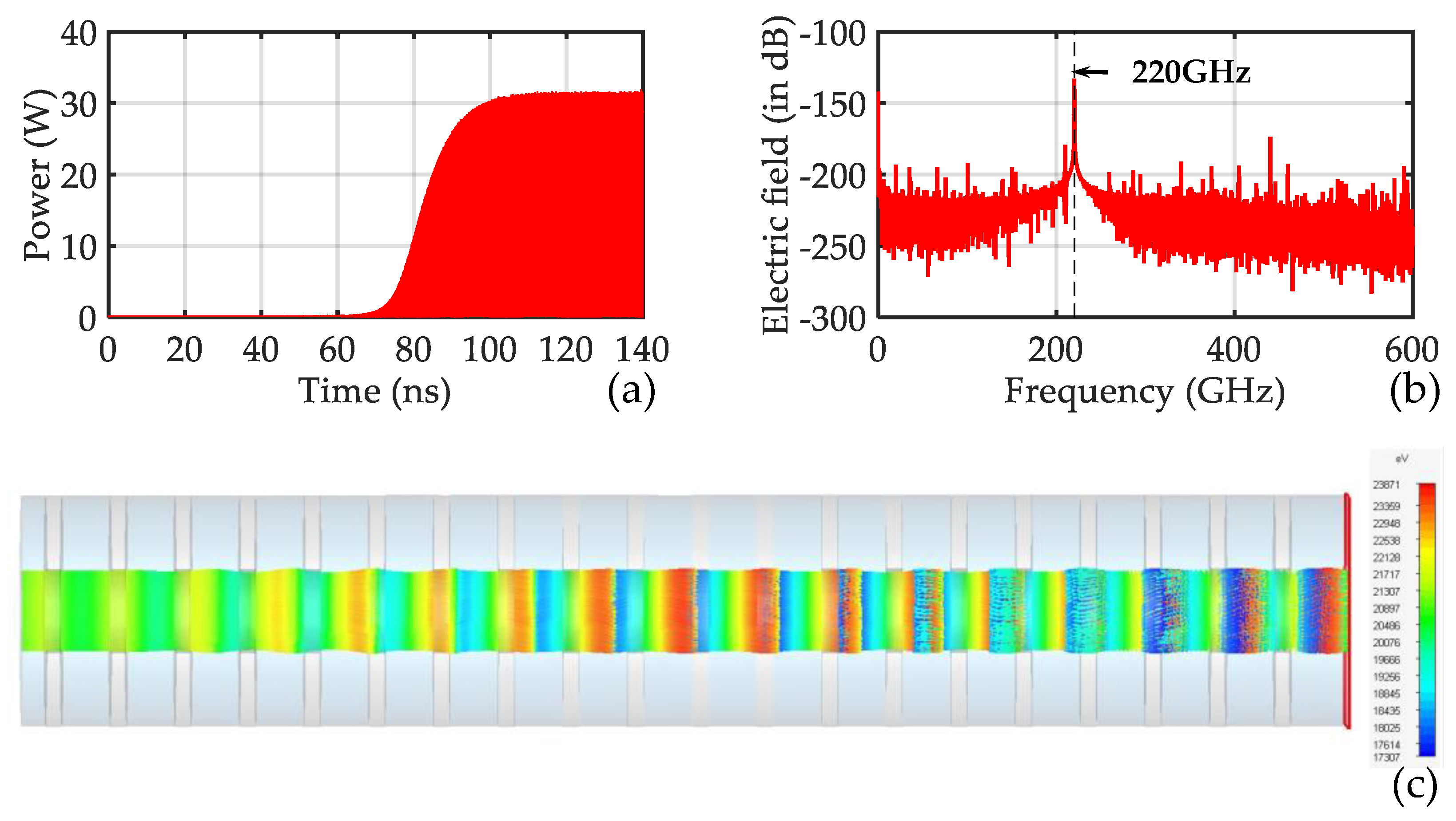
In this structure, the electron beam has a radius of 0.2 mm and an emission current of 50 mA, with an electron beam radius of 0.18 mm having been obtained upon optimization. Typical particle-in-cell (PIC) results of the BWO are shown in Figure 7, with the operating beam voltage set to 21 kV. As is shown in Figure 7a, after stable oscillation, a 32 W, 220 GHz output wave is obtained. Figure 7b,c presents the output signal spectrum showing mode purity and electron beam bunching. As an ordinary type (O-type) VED, BWO employs a magnetically focused electron beam. With the beam-wave interaction between the electron beam and the specify frequency of electromagnetic wave, electron bunching occurs in the SWS, as shown in Figure 7c. The energy extracted from the slowing electrons is transferred to the electromagnetic wave.
3. Results and Discussion
It is demonstrated in this work that a cold cathode terahertz BWO can be realized using CNTs as cold cathode field electron emitters. In principle, there is no major difficulty in our cold cathode BWO design to further increase output radiation frequency to higher end of the terahertz range. In the dual-gridded CNT-based cold cathode electron gun, a circular electron beam with maximum beam current of 50 mA (beam current density of 58.5 A/cm2) and beam radius of 0.18 mm is achieved on the output port. Our findings indicate that this kind of electron gun is completely suitable to apply to higher output power and higher radiation frequency terahertz BWOs.
In addition, we aim to further optimize the dual-gridded CNT-based cold cathode electron gun design in order to improve performance, such as dramatically uniform, larger emission current and emission current density, and a greater compression ratio. Such high-performance electron sources will facilitate the development of ultra-high-output power terahertz radiation sources in the future.
4. Conclusions
A dual-gridded field emission architecture based on CNT cold cathode is investigated here to solve the non-uniform electric field distribution at the cathode surface, which is the major cause of cathode arcing. High-emission current density electron beams with a transparency of 100% have been achieved using the proposed unique topology. Furthermore, a CNT cold cathode electronic optical system based on a dual-gridded field emission structure has been designed with a high-compression ratio of 39. The high-quality electron beam current density, correspondingly, was increased by a substantial amount, satisfying the 0.22 THz BWO operational design. Finally, the 0.22 THz disk-loaded waveguide BWO with a 32 W output power at an operating voltage of 21 kV was obtained by exploiting the high-performance CNT-based electronic optical system.
Our studies also suggest that the size of the proposed dual-gridded architecture can be changed from the μm to the mm scale, and the emission current will be augmented accordingly. Our findings suggest that the spatial architecture, and therefore the emission current, can be tailored for the development of high-power millimetre-wave VEDs. In addition, the dual-gridded architecture can be modified asymmetrically to generate high-aspect-ratio, sheet-beam VEDs. The high-compression-ratio, dual-gridded CNT electron gun, as a new structure towards new VED paradigms, shows much potential not only in traditional backward wave oscillators but also in traveling wave tubes, extended-interaction klystrons, and extended-interaction oscillators. In the future, further experiments will be conducted to verify the present simulation results. This study provides a positive outlook towards the realization of CNT-based, cold cathode, terahertz, vacuum electronic radiation sources.
Author Contributions
Conceptualization, X.Y., Q.C., and Y.Y.; Data curation, X.Y., Q.C., M.T.C., Y.Z., L.M., and Y.Y.; Formal analysis, X.Y., Q.C., Y.Z., and Y.Y.; Investigation, X.Y. and Q.C.; Methodology, X.Y., Q.C., and M.T.C.; Project administration, X.Y., L.M., and Y.Y.; Resources, X.Y., M.T.C., and Y.Z.; Software, X.Y. and Q.C.; Supervision, X.Y. and Y.Y.; Validation, X.Y.; Visualization, X.Y. and Y.Y.; Writing—original draft, X.Y. and Q.C.; Writing—review & editing, M.T.C., Y.Z., L.M., and Y.Y.
Funding
This research was funded by the National Natural Science Foundation of China, grant number 61771096; Fundamental Research Funds for the Central Universities, grant number ZYGX2016J059; and National Basic Research Program of China, grant number 2013CB933603.
Conflicts of Interest
The authors declare no conflict of interest.
References
- Booske, J.H.; Dobbs, R.J.; Joye, C.D.; Kory, C.L.; Neil, G.R.; Park, G.S.; Park, J.; Temkin, R.J. Vacuum electronic high power terahertz sources. IEEE Trans. Terahertz Sci. Technol. 2011, 1, 54–75. [Google Scholar] [CrossRef]
- Baughman, W.E.; Yokus, H.; Balci, S.; Wilbert, D.S.; Kung, P.; Kim, S.M. Observation of hydrofluoric acid burns on osseous tissues by means of terahertz spectroscopic imaging. IEEE Trans. Terahertz Sci. Technol. 2013, 3, 387–394. [Google Scholar] [CrossRef]
- Ostmann, T.K.; Jastrow, C.; Baaske, K.; Heinen, B.; Schwerdtfeger, M.; Kärst, U.; Hintzsche, H.; Stopper, H.; Koch, M.; Schrader, T. Field exposure and dosimetry in the THz frequency range. IEEE Trans. Terahertz Sci. Technol. 2014, 4, 12–25. [Google Scholar] [CrossRef]
- Komandin, G.A.; Chuchupal, S.V.; Lebedev, S.P.; Goncharov, Y.G.; Korolev, A.F.; Porodinkov, O.E.; Spektor, I.E.; Volkov, A.A. BWO generators for terahertz dielectric measurements. IEEE Trans. Terahertz Sci. Technol. 2013, 3, 440–444. [Google Scholar] [CrossRef]
- Suen, J.Y.; Fang, M.T.; Lubin, P.M. Global distribution of water vapor and cloud cover—Sites for high-performance THz applications. IEEE Trans. Terahertz Sci. Technol. 2014, 4, 86–100. [Google Scholar] [CrossRef]
- Maestrini, A.; Mehdi, I.; Siles, J.V.; Ward, J.S.; Lin, R.; Thomas, B.; Lee, C.; Gill, J.; Chattopadhyay, G.; Schlecht, E.; et al. Design and characterization of a room temperature all-solid-state electronic source tunable from 2.48 to 2.47 THz. IEEE Trans. Terahertz Sci. Technol. 2012, 2, 177–185. [Google Scholar] [CrossRef]
- Otsuji, T.; Popov, V.; Ryzhii, V. Active graphene plasmonics for terahertz device applications. J. Phys. D Appl. Phys. 2014, 47, 125–134. [Google Scholar] [CrossRef]
- Sharma, R.; Schrottke, L.; Wienold, M.; Biermann, K.; Tahraoui, A.; Grahn, H.T. Influence of post-growth rapid thermal annealing on the transport and lasing characteristics of terahertz quantum-cascade lasers. J. Phys. D Appl. Phys. 2013, 46, 305107. [Google Scholar] [CrossRef]
- Gong, H.; Travish, G.; Xu, J.; Wei, Y.; Feng, J.; Gong, Y. High-power tunable terahertz radiation by high-order harmonic generation. IEEE Trans. Electron Devices 2013, 60, 482–486. [Google Scholar] [CrossRef]
- Booske, J.H. Plasma physics and related challenges of millimeter-wave-to-terahertz and high power microwave generation. Phys. Plasmas 2008, 15, 055502. [Google Scholar] [CrossRef]
- Parker, R.K.; Abrams, R.H.; Danly, B., Jr.; Levush, B. Vacuum electronics. IEEE Trans. Microw. Theory Tech. 2002, 50, 835–845. [Google Scholar] [CrossRef]
- Xu, C.; Yin, Y.; Bi, L.; Zhang, Z.; Chang, Z.; Rauf, A.; Ullah, S.; Wang, B.; Meng, L. A novel wire-wrap slow-wave structure for terahertz backward wave oscillator applications. IEEE Trans. Electron Devices 2017, 64, 293–299. [Google Scholar] [CrossRef]
- Liu, Q.; Wang, Z.; Liu, P.; Du, C.; Li, H.; Xu, A. A THz backward-wave oscillator based on a double-grating rectangular waveguide. IEEE Trans. Electron Devices 2013, 60, 1463–1468. [Google Scholar] [CrossRef]
- Zhang, M.; Wei, Y.; Shi, X.; Yue, L.; Wei, W.; Xu, J.; Zhao, G.; Huang, M.; Wang, Z.; Gong, Y.; et al. A modified slow-wave structure for backward-wave oscillator design in THz band. IEEE Trans. Electron Devices 2014, 4, 741–748. [Google Scholar] [CrossRef]
- Mineo, M.; Paoloni, C. Corrugated rectangular waveguide tunable backward wave oscillator for terahertz applications. IEEE Trans. Electron Devices 2010, 57, 1481–1484. [Google Scholar] [CrossRef]
- Collins, C.M.; Parmee, R.J.; Milne, W.I.; Cole, M.T. High performance field emitters. Adv. Sci. 2016, 3, 1500318. [Google Scholar] [CrossRef] [PubMed]
- Milne, W.I.; Teo, K.B.K.; Minoux, E.; Groening, O.; Gangloff, L.; Hudanski, L.; Schnell, J.-P.; Dieumegard, D.; Peauger, F.; Bu, I.Y.Y.; et al. Aligned carbon nanotubes/fibers for applications in vacuum microwave amplifiers. J. Vac. Sci. Technol. B 2006, 24, 345–348. [Google Scholar] [CrossRef]
- Kim, H.J.; Choi, J.J.; Han, J.-H.; Park, J.H.; Yoo, J.-B. Design and field emission test of carbon nanotube pasted cathodes for traveling wave tube applications. IEEE Trans. Electron Devices 2006, 53, 2674–2680. [Google Scholar] [CrossRef]
- Ulisse, G.; Brunetti, F.; Tamburri, E.; Orlanducci, S.; Cirillo, M.; Terranova, M.L.; Carlo, A.D. Carbon nanotube cathodes for electron gun. IEEE Electron Device Lett. 2013, 34, 698–700. [Google Scholar] [CrossRef]
- Manohara, H.M.; Toda, R.; Lin, H.R.; Liao, A.; Bronikowski, M.J.; Siegel, P.H. Carbon nanotube bundle array cold cathodes for THz vacuum tube sources. J. Infrared Millim. Terahertz Waves 2009, 30, 1338–1350. [Google Scholar] [CrossRef]
- Yuan, X.; Zhu, W.; Zhang, Y.; Xu, N.; Yan, Y.; Wu, J.; Shen, Y.; Chen, J.; She, J.; Deng, S. A Fully-sealed carbon-nanotube cold-cathode terahertz gyrotron. Sci. Rep. 2016, 6, 32936. [Google Scholar] [CrossRef] [PubMed]
- Yuan, X.; Zhang, Y.; Cole, M.T.; Yan, Y.; Li, X.; Parmee, R.; Wu, J.; Xu, N.; Milne, W.I.; Deng, S. A truncated-cone carbon nanotube cold-cathode electron gun. Carbon 2017, 120, 374–379. [Google Scholar] [CrossRef]
- Yuan, X.; Zhang, Y.; Yang, H.; Li, X.; Xu, N.; Deng, S.; Yan, Y. A Gridded high-compression-ratio carbonnanotube cold cathode electron gun. IEEE Electron Device Lett. 2015, 36, 399–401. [Google Scholar] [CrossRef]
- Yuan, X.; Wang, B.; Cole, M.T.; Zhang, Y.; Deng, S.; Milne, W.I.; Yan, Y. Theoretical Research on a multibeam-modulated electron gun based on carbon nanotube cold cathodes. IEEE Trans. Electron Devices 2016, 62, 2919–2924. [Google Scholar] [CrossRef]
- Chen, Q.; Yuan, X.; Zhang, Y.; Li, H.; Wang, B.; Yan, Y.; Meng, L. Study on a high beam transparency gridded X-ray electron gun based on carbon nanotube cold cathode. J. Nanoelectron. Optoelectron. 2018, 13, 1265–1270. [Google Scholar] [CrossRef]
- Li, C.; Zhang, Y.; Mann, M.; Hasko, D.; Lei, W.; Wang, B.; Chu, D.; Pribat, D.; Amaratunga, G.A.J.; Milne, W.I. High emission current density, vertically aligned carbon nanotube mesh, field emitter array. Appl. Phys. Lett. 2010, 97, 113107. [Google Scholar] [CrossRef]
- Faillon, G.; Kornfeld, G.; Bosch, E.; Thumm, M.K. Microwave Tubes. In Vacuum Electronics; Eichmeier, J.A., Thumm, M.K., Eds.; Springer: Berlin/Heidelberg, Germany, 2008; Volume 3, pp. 1–84. [Google Scholar]
- Benford, J.; Swegle, J.A.; Schamiloglu, E. High Power Microwaves, 2nd ed.; Taylor and Francis Group: New York, NY, USA, 2007; pp. 321–370. [Google Scholar]
- Nashed, A.I.; Chaudhuri, S.K.; Safavi-Naeini, S. A 650-GHz backward wave oscillator based on axial loaded double defected-photonic crystal SWS. IEEE Trans. Plasma Sci. 2017, 45, 372–380. [Google Scholar] [CrossRef]
Figure 1.
Schematic of the dual-gridded field emission structure based on carbon nanotube (CNT) cold cathode. SSG: second separating grid; FSG: first separating grid.
Figure 1.
Schematic of the dual-gridded field emission structure based on carbon nanotube (CNT) cold cathode. SSG: second separating grid; FSG: first separating grid.

Figure 2.
Surface electric field intensity as a function of first separating grid mesh hole h1. (a) Electric field intensity at square cathode surface. Inset: Schematic drawing of dual-gridded system. (b) Expanded view of the central unit CNT cathode surface electric field intensity.
Figure 2.
Surface electric field intensity as a function of first separating grid mesh hole h1. (a) Electric field intensity at square cathode surface. Inset: Schematic drawing of dual-gridded system. (b) Expanded view of the central unit CNT cathode surface electric field intensity.

Figure 3.
Fitting and experimental emission current density as a function of applied electric field. Insets from Ref. [26]: (a) top view scanning electron microscope (SEM) image of the as-grown honeycomb structure CNT mesh. (b) Cross sectional SEM image of the CNT array showing uniform, high density, and vertically aligned CNTs.

Figure 4.
Beam trajectories within the dual-gridded, CNT-based electron gun. (a) Simulated beam trajectories. (b) Expanded view of the dual-gridded system; there is no electron interception. (c) CNT cold cathode emission area. (d) Electron beam spot size in the anode plane. (e) Magnetic field intensity profile along the tube central axis.

Figure 5.
Cross-sectional illustration of dual-gridded CNT, cold-cathode, terahertz, disk-loaded waveguide backward wave oscillator (BWO).
Figure 5.
Cross-sectional illustration of dual-gridded CNT, cold-cathode, terahertz, disk-loaded waveguide backward wave oscillator (BWO).

Figure 6.
Electric field distribution of the TM01 mode on the cross section at the center of (a) transverse-plane and (b) longitudinal-plane. (c) The TM01 mode dispersion curve as a function of the normalized wavenumber. (d) Transmission characteristic.
Figure 6.
Electric field distribution of the TM01 mode on the cross section at the center of (a) transverse-plane and (b) longitudinal-plane. (c) The TM01 mode dispersion curve as a function of the normalized wavenumber. (d) Transmission characteristic.

Figure 7.
The presentation of the particle-in-cell (PIC) results after beam-wave interaction stable with operation voltage 21 kV: (a) signal power amplitude at output port, (b) output signal spectrum showing mode purity, and (c) electron bunch phenomenon.
Figure 7.
The presentation of the particle-in-cell (PIC) results after beam-wave interaction stable with operation voltage 21 kV: (a) signal power amplitude at output port, (b) output signal spectrum showing mode purity, and (c) electron bunch phenomenon.


Table 1.
Dimensions of dual-gridded field emission structure based on CNT cold cathode.
| Symbols | Parameters | Values and Units |
|---|---|---|
| rc | Cathode substrate radius | 1.116 mm |
| h1 | Mesh hole of the FSG | 0.12 mm |
| h2 | Mesh hole of the SSG | 0.13 mm |
| w1 | Wire line of the FSG | 0.02 mm |
| w2 | Wire line of the SSG | 0.01 mm |
| t1 | Thickness of the FSG | 0.02 mm |
| t2 | Thickness of the SSG | 0.02 mm |
| d1 | Distance between CNT and SSG | 0.1 mm |
| Uc | Cathode voltage | 0 |
| U2 | SSG voltage | 0.5 kV |
Table 2.
BWO operating paramenters.
| Symbols | Parameters | Values and Units |
|---|---|---|
| d | Circular waveguide inner diameter | 1.054 mm |
| t | Disk inner diameter | 0.4 mm |
| w | Disk width | 0.076 mm |
| p | Period length | 0.3044 mm |
| f | Operating frquency | 0.22 THz |
| U | Operating voltage | 21 kV |
| I | Operating current | 50 mA |
© 2018 by the authors. Licensee MDPI, Basel, Switzerland. This article is an open access article distributed under the terms and conditions of the Creative Commons Attribution (CC BY) license (http://creativecommons.org/licenses/by/4.0/).
Share and Cite
MDPI and ACS Style
Chen, Q.; Yuan, X.; Cole, M.T.; Zhang, Y.; Meng, L.; Yan, Y. Theoretical Study of a 0.22 THz Backward Wave Oscillator Based on a Dual-Gridded, Carbon-Nanotube Cold Cathode. Appl. Sci. 2018, 8, 2462. https://doi.org/10.3390/app8122462
AMA Style
Chen Q, Yuan X, Cole MT, Zhang Y, Meng L, Yan Y. Theoretical Study of a 0.22 THz Backward Wave Oscillator Based on a Dual-Gridded, Carbon-Nanotube Cold Cathode. Applied Sciences. 2018; 8(12):2462. https://doi.org/10.3390/app8122462
Chicago/Turabian StyleChen, Qingyun, Xuesong Yuan, Matthew T. Cole, Yu Zhang, Lin Meng, and Yang Yan. 2018. "Theoretical Study of a 0.22 THz Backward Wave Oscillator Based on a Dual-Gridded, Carbon-Nanotube Cold Cathode" Applied Sciences 8, no. 12: 2462. https://doi.org/10.3390/app8122462
Note that from the first issue of 2016, this journal uses article numbers instead of page numbers. See further details here.