Unidirectional Slow Light Transmission in Heterostructure Photonic Crystal Waveguide


1
Wuhan National Laboratory for Optoelectronics, Huazhong University of Science and Technology, Wuhan 430074, China
2
Department of Electrical and Computer Engineering, McMaster University, Hamilton, ON L8S 4K1, Canada
*
Author to whom correspondence should be addressed.
Appl. Sci. 2018, 8(10), 1858; https://doi.org/10.3390/app8101858
Submission received: 9 September 2018
/
Revised: 5 October 2018
/
Accepted: 7 October 2018
/
Published: 9 October 2018
(This article belongs to the Special Issue Substrate Integrated Waveguide (SIW) and Its Applications)
Abstract
:Featured Application
The proposed unidirectional backscattering-immune device may provide a potential way to realize robust optical delay lines and robust on-chip optical buffers.
Abstract
In conventional photonic crystal systems, extrinsic scattering resulting from random manufacturing defects or environmental changes is a major source of loss that causes performance degradation, and the backscattering loss is amplified as the group velocity slows down. In order to overcome the limitations in slow light systems, we propose a backscattering-immune slow light waveguide design. The waveguide is based on an interface between a square lattice of magneto-optical photonic crystal with precisely tailored rod radii of the first two rows and a titled 45 degrees square lattice of Alumina photonic crystal with an aligned band gap. High group indices of 77, 68, 64, and 60 with the normalized frequency bandwidths of 0.444%, 0.481%, 0.485%, and 0.491% are obtained, respectively. The corresponding normalized delay-bandwidth products remain around 0.32 for all cases, which are higher than previously reported works based on rod radius adjustment. The robustness for the edge modes against different types of interfacial defects is observed for the lack of backward propagation modes at the same frequencies as the unidirectional edge modes. Furthermore, the transmission direction can be controlled by the sign of the externally applied magnetic field normal to the plane.
1. Introduction
The velocity of light in vacuum is approximately , fast enough to circle the Earth once in 0.3 s. However, faster is not always better, such an ultrahigh speed makes it very difficult to control the optical signals in time domain [1,2]. Slow light with a much slower group velocity makes it possible to delay and temporarily store light in all-optical systems [3,4,5,6]. Among all the approaches to realize slow light, photonic crystal waveguide (PCW) has drawn much attention as it supports room temperature operation and is compatible with on-chip integration [7,8,9,10,11,12,13,14,15,16]. However, the performance of the conventional photonic crystal (PC) systems is very vulnerable to the backscattering loss induced by disorders or defects [17,18]. The backscattering loss is amplified as the group velocity slows down in the waveguide [19,20].
The development of the photonic chiral edge state (CES) [21,22,23,24] may provide an approach to overcome the limitations related to backscattering loss in slow light systems, as it is robust against scattering from interfacial defects. The existence of the photonic CESs at the interface of a two-dimensional (2D) magneto-optical photonic crystal (MOPC) was first theoretically proposed by Haldane [25,26] and was then experimentally verified by Wang et al. [27,28] in microwave regime. Since the CESs are leaky in the free space [21,29], a regular PC with an aligned band gap has to be bounded to the interface of the MOPC to prevent the radiation leakage. The constructed waveguide only supports unidirectional modes as it has only positive (negative) group velocities and the backscattering is completely suppressed. This enabled the light transmission to be immune to fabrication imperfections. The unidirectional transmission feature is of great significance for slow light systems and may provide robust designs for optical delay and light storage applications [30].
There are various approaches to tailor the dispersion curves to realize slow light in PC systems: modification the radii of air holes [31], shifting the air holes to specific directions [32], infiltrating optical fluid into the air holes [33], infiltrating microfluidic selectively [34,35], using asymmetric engineering structure [36], merging coupled cavities [37] and, introducing alternative rows of ellipse-holes [38]. In all the above mentioned ways, adjusting the rod radius is relatively easy to control and have less fabrication issues.
In this paper, we propose a unidirectional backscattering-immune slow light waveguide. The waveguide is constructed by a square lattice of MOPC with the rod radii of the first two rows adjacent to the waveguide core are precisely tailored and a titled 45° square lattice of Alumina PC as an ancillary cladding. A flat band for slow light is obtained and the slope (group velocities) of the waveguide dispersion curves process only positive (or only negative) values, which is determined by the sign of the externally applied magnetic field. In the waveguide, the backscattering is completely suppressed for the lack of the backward transmission channel. This unique feature ensures that the design can avoid performance degradation induced by impurities or defects, which is difficult to realize in conventional slow light systems.
The remaining content of this work is arranged as follows: to better understand the content of the subsequent sections, we briefly introduce the theoretical background of slow light in Section 2. In Section 3, we firstly introduce the design of the unidirectional slow light waveguide and then exhibit the slow light characteristics and the backscattering-immune properties of the waveguide in detail. The followed simulation results are based on the finite element method (FEM).
2. Theoretical Background
The group velocity (or equivalently the group index , denotes the speed of light in vacuum) is not the only key parameter to evaluate the performance of slow light devices. We should also take into account the frequency bandwidth, group velocity dispersion (GVD), and the propagation loss. The frequency bandwidth and the group index are encapsulated by the normalized delay-bandwidth product (NDBP) [16,39]. The NDBP indicates the obtained compromise between a large operating bandwidth and a large group index, as given by
is an average group index in the desired slow light bandwidth. denotes the normalized frequency bandwidth, where represents the difference between the maximum and the minimum frequency in the slow light region and represents the center frequency. The reduction of should be balanced with the bandwidth requirements in practical applications. The frequency bandwidth is considered as the frequency range corresponding to a group index variation with respect to the obtained mean value [16,39,40].
The group velocity is strongly dependent on the operation frequencies [41,42], as quantified by the second-order derivative of the dispersion relation:
is the GVD parameter. Large can lead to pulse distortion, and thereby degrades the performance of the slow light device. Taking the practical application requirements into consideration, the GVD parameter should below the order of [43,44] ( is the lattice constant in PC systems).
The propagation loss, mainly due to light scattering, is the most critical limitations to be solved in slow light systems. The scattering loss is mainly due to random fabrication imperfections or environmental changes. It increases quadratically with the reduced as proposed theoretically in [19] and certified experimentally in [20]. If the propagation loss penalty is too high, the superiority of slow light might be compromised. To overcome this crucial limitation in slow light systems, we propose a backscattering-immune slow light waveguide as demonstrated in the followed sections.
3. Model Design and Simulation Results
3.1. The Unidirectinal Waveguide and the Edge Modes
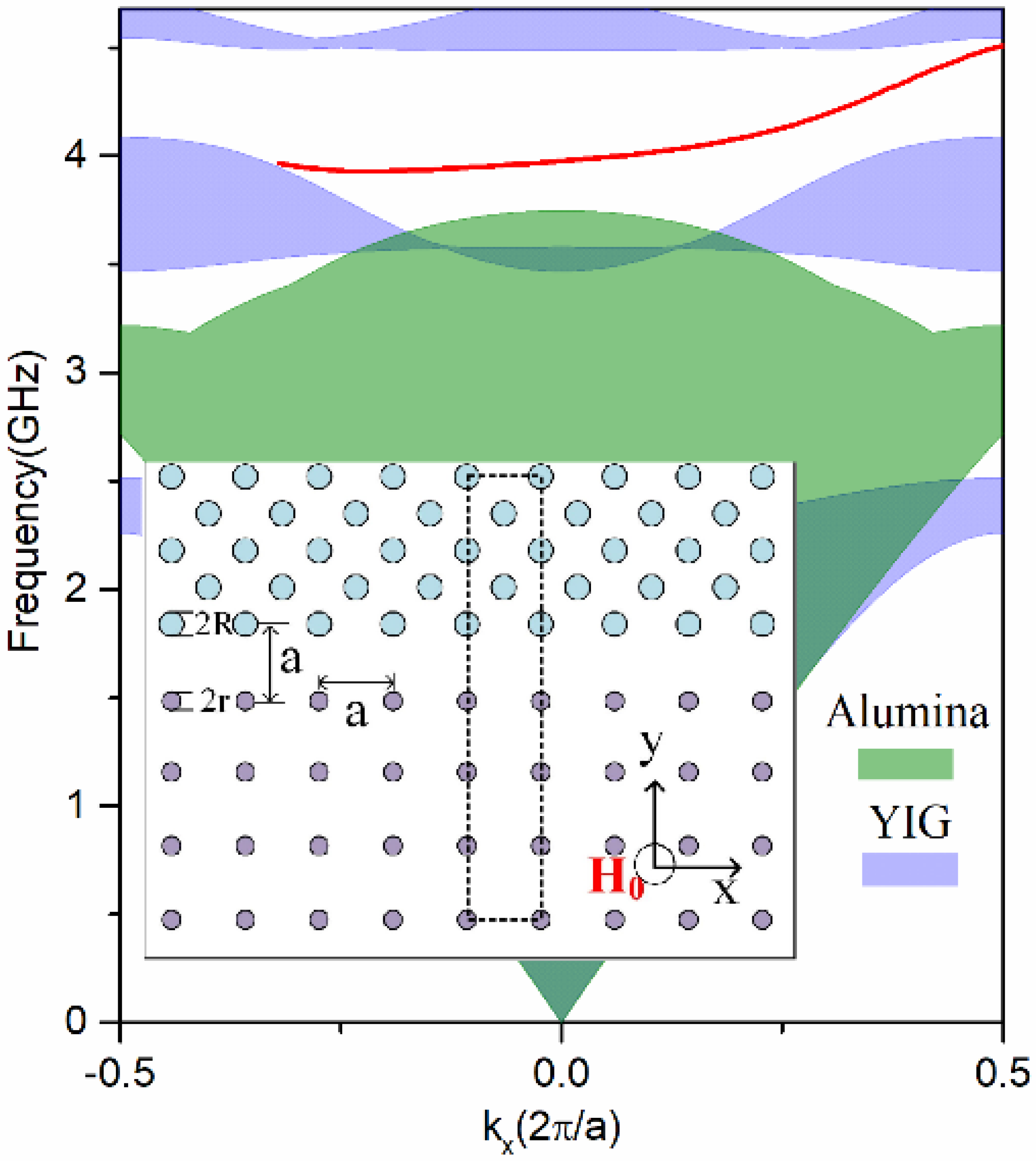
Our proposed design is based on an interface between two types of PC structures and the schematic configuration is depicted in the inset in Figure 1. The lower half plane is a square lattice of MOPC consisting of Yttrium–Iron–Garnet (YIG) rods [28], where is the lattice constant. With an externally applied magnetic field normal to the plane (along the direction), the induced magnetic permeability sensor is given as [45]
Here and indicate the operating frequency of the microwave field, the procession resonance frequency and the characteristic frequency, respectively ( is the gyromagnetic ratio). The saturation magnetization of the YIG rods is . If the external magnetic field applied along direction, both and change signs accordingly. According to Equation (4), it can be inferred that remains unchanged, but becomes its opposite value. As the edge modes at the interface of the MOPC exist inside the light cone and thus will be leaky in the free space. A titled 45° square lattice of Alumina PC (the upper half plane) with an aligned band gap has to be attached to the interface of the MOPC. Therefore, the excited edges are evanescent in both two types of PC structures.
The dashed rectangle in the inset in Figure 1 indicates a supercell of the waveguide. Using a finite element eigenfrequency analysis and imposing period boundary conditions at the supercell’s borders, we can get the band diagram of the waveguide. Theoretically, the supercell must contain infinite rods in y direction, while a supercell of 10 × 1 unite cells of the waveguide can satisfy the accuracy requirements in practical calculations. With an externally applied magnetic field along the direction, the projected band diagram of the unidirectional waveguide for transverse magnetic (TM) modes (electric field is polarized along z-axis) are given in Figure 1. The shadow regions are the bulk modes of full MOPC and Alumina PC and the red curve denotes the unidirectional edge mode. As shown in Figure 1, the slope of the red curve (group velocities) has only positive values. It indicates that the waveguide support only forward transmission and the opposite propagation is completely prohibited. This unique feature insures that the edge modes are robust against interfacial disorders or defects. It is of significant importance for slow light systems.
3.2. Slow Light Properties
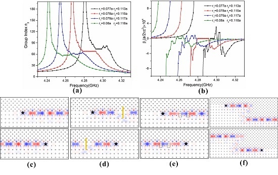
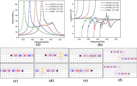
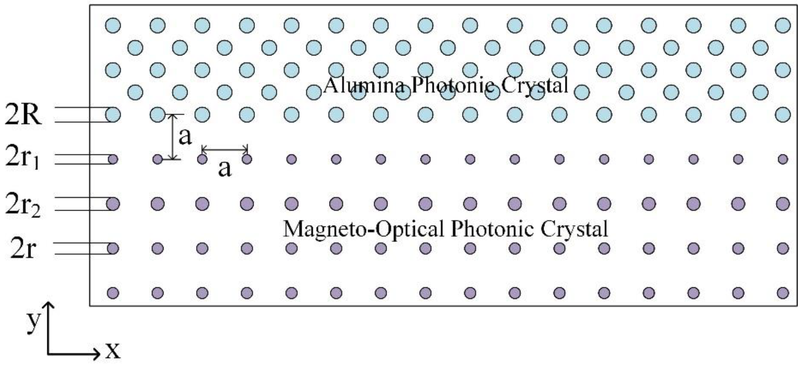
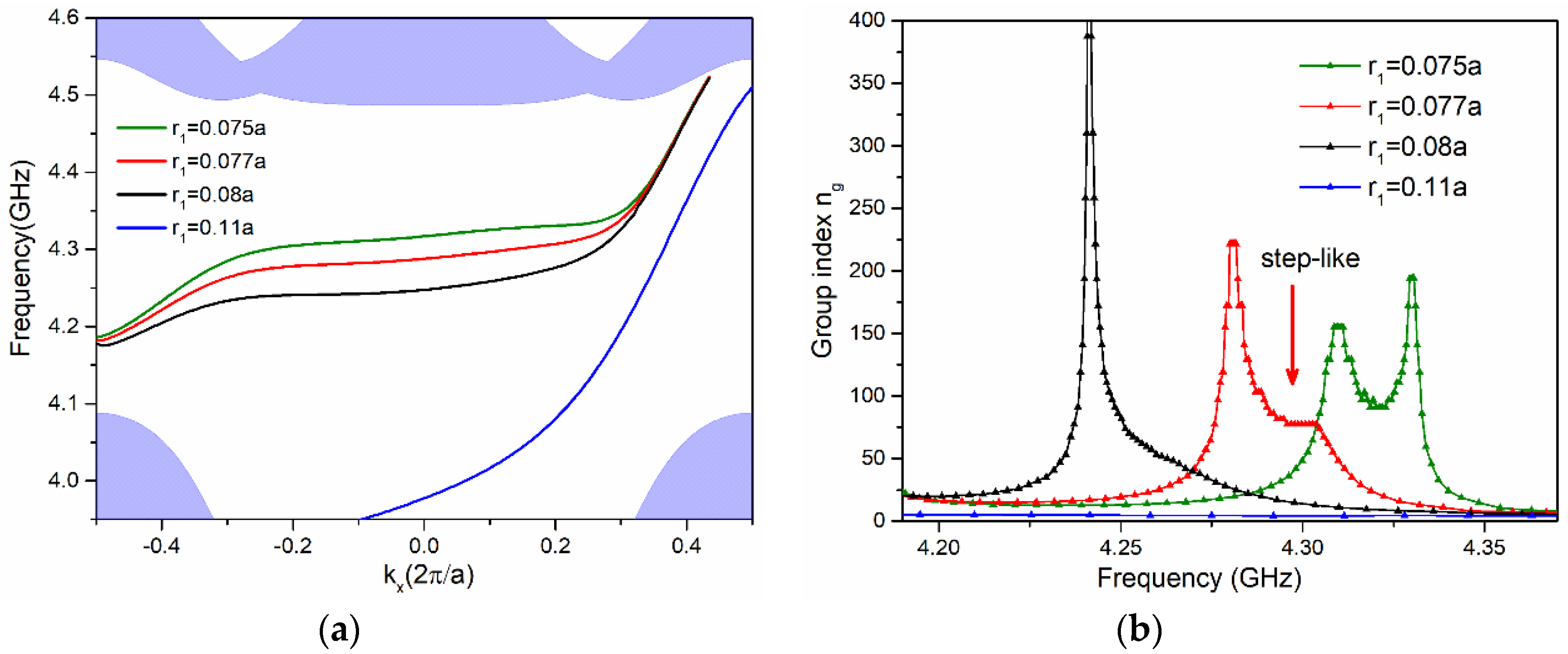
Since the first few rows of YIG rods have the greatest influence on the shape of the dispersion curve, we adjust the radii of the YIG rods to obtain a flat band region for slow light (a large NDBP value and a low GVD value) with the unidirectional feature. The new configuration of the waveguide is shown in Figure 2, the radii of the YIG rods in the first and second rows adjacent to the waveguide core are denoted by and , respectively. We perform a serious of numerical simulations for different values and find that when goes beyond the range of to , the unique unidirectionality of the edge modes vanishes. Therefore, we present the dispersion diagram for parameters , , , and , as shown in Figure 3a. The corresponding group index characteristics are illustrated in Figure 3b. The dispersion curve becomes flat at and a step-like region (corresponding to the slow light region) appears, which indicates a low GVD feature. In the cases of and , the curve gets very steep and the step-like behavior disappears.
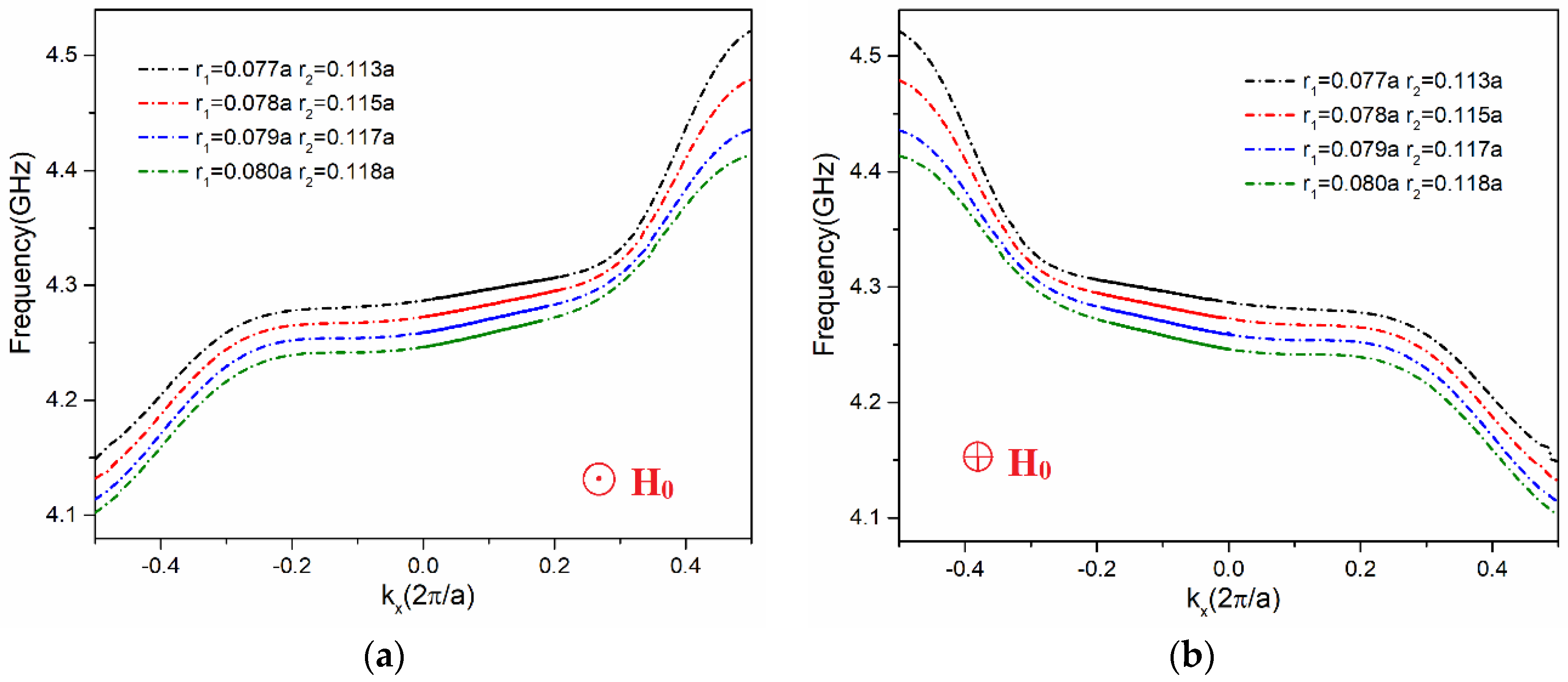
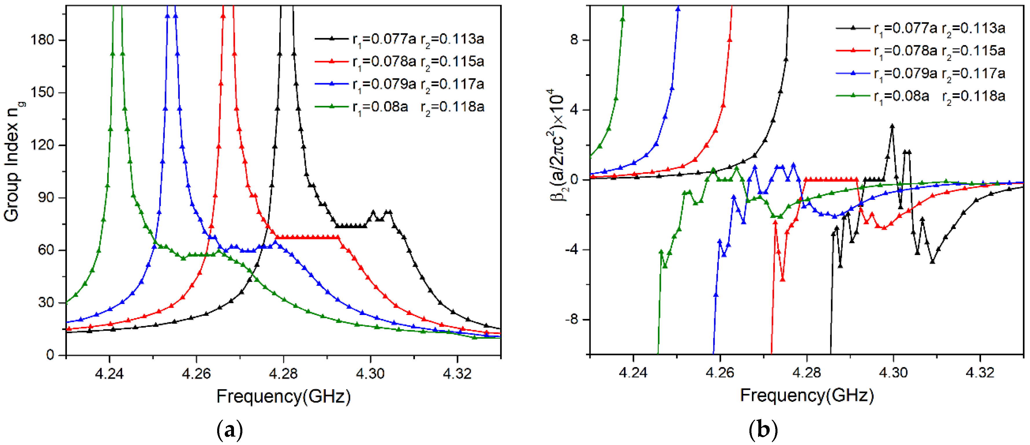
Based on the optimum , we then adjust to further engineer the dispersion curve. Figure 4a illustrates the projected band diagram of TM modes with an external magnetic field applied in the +z direction for parameters , ; , ; , ; and , . The slope of the curves (group velocities) have only positive values and the flat band regions for slow light are highlighted by the thick solid lines. The corresponding frequency range of the slow light region are 4.2886 GHz–4.3077 GHz, 4.2744 GHz–4.295 GHz, 4.2599 GHz–4.2806 GHz, and 4.2483 GHz–4.2692 GHz. The thick solid lines are approximate linear, which correspond to the step-like regions in Figure 5a. As illustrated in Figure 5a, the step-like behavior with a small change in group index in a relatively large frequency bandwidth is found in all cases, which indicates a large NDBP value and a low GVD characteristics. Under the constant group index criterion [16,40], the normalized frequency bandwidths of 0.444%, 0.481%, 0.485%, and 0.491% are obtained for group indices of 77, 68, 64, and 60, respectively. Consequently, the corresponding NDBP are 0.342, 0.327, 0.311, and 0.295 respectively. This NDBP values are higher than previous works based on modifying the rod radius [31,42,46]. The results of our design and previous works are summarized in Table 1. The corresponding GVD characteristics are illustrated in Figure 5b, we find that the GVD parameters in the slow light region keep around for all four cases. This value is two orders of magnitude smaller than the previous works [43,44] and it indicates a more superior performance of our design. In the cases of , ; , ; and , both negative values and positive values are observed, it may reveals potential applications in dispersion-compensation. Zero values is observed in the range of to (the corresponding bandwidth is 0.324%) in the case of , . The dispersion of such slow light PCW can be pursued to achieve a much slower and lower values simultaneously by further adjusting the YIG rod radii of the third row adjacent to the waveguide. Notably, when the externally applied magnetic field is reversed, the slope of the dispersion curves have only negative values as shown in Figure 3b. It indicates that the direction of the group velocity can be controlled by the external magnetic field.
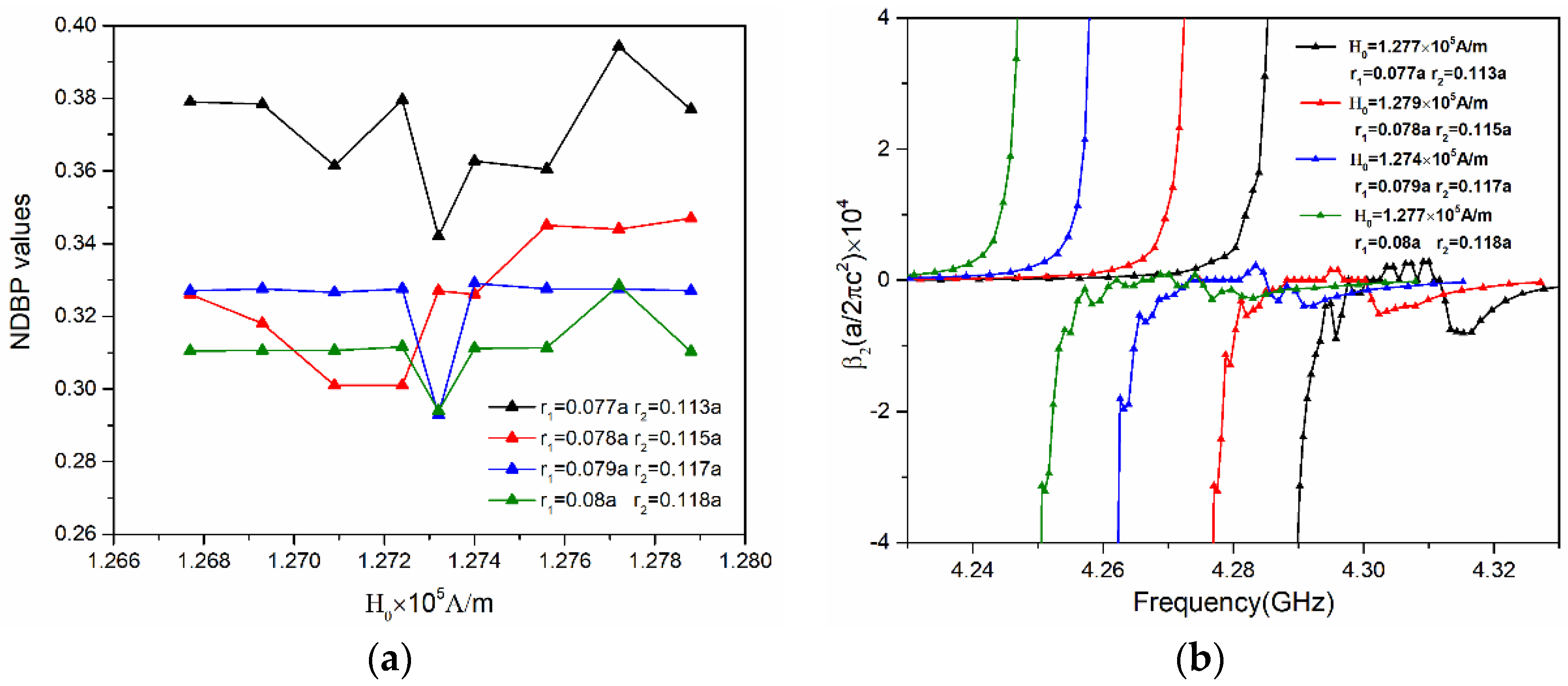
The dispersion curve can be tailored further to purse larger NDBP values by adjusting the magnitude of the externally applied magnetic field . Based on the results of Figure 5, we keep the parameters and carry out the optimizations for the . As shown in Figure 6a, corresponding to the same PCW structures in Figure 5, higher NDBP values of 0.394, 0.347, 0.329, and 0.326 are obtained for , , , and , respectively. The corresponding GVD characteristics are illustrated in Figure 6b. It is shown that the GVD parameters in the slow light region keep around for all four cases, and these values are smaller than the values in Figure 5b.
3.3. Backscattering-Immune Feature
As illustrated in Figure 4a, with an external magnetic field applied along the direction, the tailored four PCWs still have only positive group velocities (the slope of the waveguide dispersions). It indicates that the waveguide supports only forward transmission and the opposite direction transmission is completely prohibited. The absence of backward propagation channel avoids the possibility of backscattering loss and enables the electromagnetic wave to wrap around different types of obstacles as verified in Figure 7. We introduce four types of interfacial disorders into the waveguide to investigate the robustness of the edge modes. For comparison, Figure 7a shows the field distributions without introducing the disorders. As shown in Figure 7b, the light bypasses the inserted metal reflector and maintain the forward transmission. This can never happen in a conventional PCW, as the metal reflector would cause strong scattering and even block the guide mode. However, in the proposed unidirectional PCW, a new interface between the metal reflector and the MOPC is formed, thus providing a way for the electromagnetic wave to flow around the metal reflector and no backscattering takes place. The second type of defect is shown in Figure 7c, when two YIG rods at the interface of the MOPC are replaced by the Copper rods with the same size, the electromagnetic wave flow around the metal rods without introducing backscattering. The third type of defect is a Z-shaped interface, as shown in Figure 7d, the light travels along the Z-shaped interface and the forward propagation is not affected by the two sharp corners. In Figure 7e, two Alumina rods and two YIG rods at the interface of the waveguide (circled in the black rectangles) are replaced by two Alumina rods with smaller rod radii and two YIG rods with larger rod radii , respectively. It is found that the unidirectional transmission is not affected by the interfacial defects. This ideal robust unidirectional transmission feature is of great significance for slow light systems. The same unidirectionality and robustness of the edge modes from all four types of perturbation is observed when the external magnetic field is applied in the −z direction (bottom plots in Figure 7b–e). The propagation of the electromagnetic wave in the waveguide is switched to the opposite direction accordingly in all five cases.
Notably, as illustrated in the top plots of Figure 8, in all five cases, the power flow is cycling anticlockwise on the edge of the Alumina PC and clockwise on the edge of the MOPC. The opposite cycling direction of the power flow on the upper and the lower boundaries of the waveguide core may indicate the slow light properties of the unidirectional waveguide. Under the reversed externally applied magnetic field in the −z direction, the power flow is switched to the opposite direction accordingly as demonstrated in the bottom plots in Figure 8. The results in Figure 7 and Figure 8 are obtained by using a finite-element frequency domain analysis. The point source is located in the interface between two types of PC structures and perfectly matched absorbing boundary layers are applied to the surroundings of the structure in the FEM simulation.
4. Conclusions
In this paper, we propose a slow light PCW with unique unidirectionality and robustness characteristics. By choosing appropriate rod radii of the first two rods of the MOPC adjacent to the waveguide core, a high NDBP of 0.342 with a group index of 77 and frequency bandwidth of 0.444% is obtained. This value is much higher than previously reported works based on radius adjustment. The corresponding GVD parameters is zero in the range of 4.2786 GHz to 4.2925 GHz. By further adjusting the magnitude of the externally applied magnetic field, much larger NDBP values of 0.394 is obtained. Furthermore, due to the absence of the backward-propagation channel, the backscattering is completely suppressed. Our simulation results show that the edge modes are robust against the introduced interfacial defects. It is of great significance to solving the scattering loss limitations in slow light systems.
Author Contributions
Supervision, X.L.; Writing—Original Draft Preparation, Q.Z.; Writing—Review and Editing, Q.Z.
Funding
This research received no external funding.
Conflicts of Interest
The authors declare no conflict of interest.
References
- Thévenaz, L. Slow and fast light in optical fibres. Nat. Mater. 2008, 2, 474–481. [Google Scholar] [CrossRef] [Green Version]
- Krauss, T.F. Why do we need slow light. Nat. Photonics 2008, 2, 448–450. [Google Scholar] [CrossRef]
- Castellanos Munoz, M.; Petrov, A.Y.; O’Faolain, L.; Li, J.; Krauss, T.F.; Eich, M. Optically induced indirect photonic transitions in a slow light photonic crystal waveguide. Phys. Rev. Lett. 2014, 112, 053904. [Google Scholar] [CrossRef] [PubMed]
- Scullion, M.G.; Arita, Y.; Krauss, T.F.; Dholakia, K. Enhancement of optical forces using slow light in a photonic crystal waveguide. Optica 2015, 2, 816. [Google Scholar] [CrossRef]
- Yan, S.; Zhu, X.; Frandsen, L.H.; Xiao, S.; Mortensen, N.A.; Dong, J.; Ding, Y. Slow-light-enhanced energy efficiency for graphene microheaters on silicon photonic crystal waveguides. Nat. Commun. 2017, 8, 14411. [Google Scholar] [CrossRef] [PubMed] [Green Version]
- Monat, C.; Grillet, C.; Collins, M.; Clark, A.; Schroeder, J.; Xiong, C.; Li, J.; O’Faolain, L.; Krauss, T.F.; Eggleton, B.J.; et al. Integrated optical auto-correlator based on third-harmonic generation in a silicon photonic crystal waveguide. Nat. Commun. 2014, 5, 3246. [Google Scholar] [CrossRef] [PubMed] [Green Version]
- Zhao, Y.; Zhang, Y.N.; Qi Wang, M.; Hu, H. Review on the Optimization Methods of Slow Light in Photonic Crystal Waveguide. IEEE Trans. Nanotechnol. 2015, 14, 407–426. [Google Scholar] [CrossRef]
- Tamura, T.; Kondo, K.; Terada, Y.; Hinakura, Y.; Ishikura, N.; Baba, T. Silica-Clad Silicon Photonic Crystal Waveguides for Wideband Dispersion-Free Slow Light. J. Lightw. Technol. 2015, 33, 3034–3040. [Google Scholar] [CrossRef]
- Serna, S.; Colman, P.; Zhang, W.; Le Roux, X.; Caer, C.; Vivien, L.; Cassan, E. Experimental GVD engineering in slow light slot photonic crystal waveguides. Sci. Rep. 2016, 6, 26956. [Google Scholar] [CrossRef] [PubMed] [Green Version]
- Passoni, M.; Gerace, D.; O’Faolain, L.; Andreani, L.C. Optimizing band-edge slow light in silicon-on-insulator waveguide gratings. Opt. Exp. 2018, 26, 8470–8478. [Google Scholar] [CrossRef] [PubMed]
- Kondo, K.; Tatebe, T.; Hachuda, S.; Abe, H.; Koyama, F.; Baba, T. Fan-beam steering device using a photonic crystal slow-light waveguide with surface diffraction grating. Opt. Lett. 2017, 42, 4990–4993. [Google Scholar] [CrossRef] [PubMed]
- Elshahat, S.; Khan, K.; Yadav, A.; Bibbò, L.; Ouyang, Z. Slow-light transmission with high group index and large normalized delay bandwidth product through successive defect rods on intrinsic photonic crystal waveguide. Opt. Commun. 2018, 418, 73–79. [Google Scholar] [CrossRef]
- Ebnali-Heidari, A.; Prokop, C.; Heidari, M.E.; Karnutsch, C. A Proposal for Loss Engineering in Slow-Light Photonic Crystal Waveguides. J. Lightw. Technol. 2015, 33, 1905–1912. [Google Scholar] [CrossRef]
- Minkov, M.; Savona, V. Wide-band slow light in compact photonic crystal coupled-cavity waveguides. Optica 2015, 2, 631–634. [Google Scholar] [CrossRef]
- Schulz, S.A.; Upham, J.; O’Faolain, L.; Boyd, R.W. Photonic crystal slow light waveguides in a kagome lattice. Opt. Lett. 2017, 42, 3243–3246. [Google Scholar] [CrossRef] [PubMed]
- Tang, J.; Wang, T.; Li, X.; Wang, B.; Dong, C.; Gao, L.; Liu, B.; He, Y.; Yan, W. Wideband and Low Dispersion Slow Light in Lattice-Shifted Photonic Crystal Waveguides. J. Lightw. Technol. 2013, 31, 3188–3194. [Google Scholar] [CrossRef]
- Johnson, S.G.; Povinelli, M.L.; Soljaci, M.; Karalis, A.; Jacobs, S.; Joannopoulos, J.D. Roughness losses and volume-current methods in photonic-crystal waveguides. Appl. Phys. B 2005, 81, 283–293. [Google Scholar] [CrossRef]
- Povinelli, M.L.; Johnson, S.G.; Lidorikis, E.; Joannopoulos, J.D.; Soljačić, M. Effect of a photonic band gap on scattering from waveguide disorder. Appl. Phys. Lett. 2004, 84, 3639–3641. [Google Scholar] [CrossRef]
- Hughes, S.; Ramunno, L.; Young, J.F.; Sipe, J.E. Extrinsic optical scattering loss in photonic crystal waveguides: Role of fabrication disorder and photon group velocity. Phys. Rev. Lett. 2005, 94, 033903. [Google Scholar] [CrossRef] [PubMed]
- Kuramochi, E.; Notomi, M.; Hughes, S.; Shinya, A.; Watanabe, T.; Ramunno, L. Disorder-induced scattering loss of line-defect waveguides in photonic crystal slabs. Phys. Rev. B 2005, 72. [Google Scholar] [CrossRef]
- Ao, X.; Lin, Z.; Chan, C.T. One-way edge mode in a magneto-optical honeycomb photonic crystal. Phys. Rev. B 2009, 80, 033105. [Google Scholar] [CrossRef]
- He, C.; Sun, X.C.; Liu, X.P.; Lu, M.H.; Chen, Y.; Feng, L.; Chen, Y.F. Photonic topological insulator with broken time-reversal symmetry. Proc. Natl. Acad. Sci. USA 2016, 113, 4924–4928. [Google Scholar] [CrossRef] [PubMed]
- Khanikaev, A.B.; Mousavi, S.H.; Tse, W.-K.; Kargarian, M.; MacDonald, A.H.; Shvets, G. Photonic topological insulators. Nat. Mater. 2013, 12. [Google Scholar] [CrossRef] [PubMed]
- Lu, L.; Joannopoulos, J.D.; Soljačić, M. Topological Photonics. Nat. Photonics 2014, 8, 821–829. [Google Scholar] [CrossRef]
- Haldane, F.D.M.; Raghu, S. Possible realization of directional optical waveguides in photonic crystals with broken time-reversal symmetry. Phys. Rev. Lett. 2008, 100, 013904. [Google Scholar] [CrossRef] [PubMed]
- Raghu, S.; Haldane, F.D.M. Analogs of quantum-Hall-effect edge states in photonic crystals. Phys. Rev. A 2008, 78. [Google Scholar] [CrossRef] [Green Version]
- Wang, Z.; Chong, Y.; Joannopoulos, J.D.; Soljacic, M. Observation of unidirectional backscattering-immune topological electromagnetic states. Nature 2009, 461, 772–775. [Google Scholar] [CrossRef] [PubMed]
- Wang, Z.; Chong, Y.D.; Joannopoulos, J.D.; Soljacic, M. Reflection-free one-way edge modes in a gyromagnetic photonic crystal. Phys. Rev. Lett. 2008, 100, 013905. [Google Scholar] [CrossRef] [PubMed]
- Poo, Y.; Wu, R.X.; Lin, Z.; Yang, Y.; Chan, C.T. Experimental realization of self-guiding unidirectional electromagnetic edge states. Phys. Rev. Lett. 2011, 106, 093903. [Google Scholar] [CrossRef] [PubMed]
- Hafezi, M.; Demler, E.A.; Lukin, M.D.; Taylor, J.M. Robust optical delay lines with topological protection. Nat. Phys. 2011, 7, 907–912. [Google Scholar] [CrossRef] [Green Version]
- Kurt, H.; Üstün, K.; Ayas, L. Study of different spectral regions and delay bandwidth relation in slow light photonic crystal waveguides. Opt. Exp. 2010, 18, 26965–26977. [Google Scholar] [CrossRef] [PubMed]
- Liang, J.; Ren, L.Y.; Yun, M.J.; Han, X.; Wang, X.J. Wideband ultraflat slow light with large group index in a W1 photonic crystal waveguide. J. Appl. Phys. 2011, 110, 063103. [Google Scholar] [CrossRef]
- Pourmand, M.; Karimkhani, A.; Nazari, F. Wideband and low-dispersion engineered slow light using liquid infiltration of a modified photonic crystal waveguide. Appl. Opt. 2016, 55, 10060–10066. [Google Scholar] [CrossRef] [PubMed]
- Lü, S.; Zhao, J.; Zhang, D. Flat band slow light in asymmetric photonic crystal waveguide based on microfluidic infiltration. Appl. Opt. 2010, 49, 3930–3934. [Google Scholar] [CrossRef] [PubMed]
- Ebnali-Heidari, M.; Grillet, C.; Monat, C.; Eggleton, B.J. Dispersion engineering of slow light photonic crystal waveguides using microfluidic infiltration. Opt. Exp. 2009, 17, 1628–1635. [Google Scholar] [CrossRef]
- Nazari, F.; Samsami Khodadad, F. On chip optical isolator based on non-linear silicon photonic crystal by using asymmetric engineering waveguide. J. Mod. Opt. 2017, 64, 653–658. [Google Scholar] [CrossRef]
- Üstün, K.; Kurt, H. Ultra slow light achievement in photonic crystals by merging coupled cavities with waveguides. Opt. Exp. 2010, 20, 21155–21161. [Google Scholar] [CrossRef] [PubMed]
- Xu, Y.; Xiang, L.; Cassan, E.; Gao, D.; Zhang, X. Slow light in an alternative row of ellipse-hole photonic crystal waveguide. Appl. Opt. 2013, 52, 1155–1160. [Google Scholar] [CrossRef] [PubMed]
- Hao, R.; Cassan, E.; Kurt, H.; Roux, X.L.; Marris-Morini, D.; Vivien, L.; Wu, H.; Zhou, Z.; Zhang, X. Novel slow light waveguide with controllable delay-bandwidth product and utra-low dispersion. Opt. Exp. 2010, 18, 5492–5950. [Google Scholar] [CrossRef] [PubMed]
- Petrov, A.Y.; Eich, M. Zero dispersion at small group velocities in photonic crystal waveguides. Appl. Phys. Lett. 2004, 85, 4866–4868. [Google Scholar] [CrossRef]
- Lenz, G.; Eggleton, B.J.; Madsen, C.K.; Slusher, R.E. Optical Delay Lines Based on Optical Filters. IEEE J. Quantum Electron. 2001, 37, 525–532. [Google Scholar] [CrossRef]
- Frandsen, L.H.; Lavrinenko, A.V.; Fage-Pedersen, J.; Borel, P.I. Photonic crystal waveguides with semi-slow light and tailored dispersion properties. Opt. Exp. 2006, 14, 9444–9450. [Google Scholar] [CrossRef]
- Engelen, R.J.P.; Sugimoto, Y.; Watanabe, Y.; Korterik, J.P.; Ikeda, N.; Hulst, N.F.; Asakawa, K.; Kuipers, L. The effect of higher-order dispersion on slow light propagation in photonic crystal waveguides. Opt. Exp. 2006, 14, 1658–1672. [Google Scholar] [CrossRef] [Green Version]
- Ma, J.; Jiang, C. Demonstration of Ultraslow Modes in Asymmetric Line-Defect Photonic Crystal Waveguides. IEEE Photonics Technol. Lett. 2008, 20, 1237–1239. [Google Scholar] [CrossRef]
- Pozar, D.M. Microwave Engineering, 4st ed.; Wiley: New York, NY, USA, 2012; pp. 452–458. ISBN 978-0-470-63155-3. [Google Scholar]
- Hou, J.; Gao, D.; Wu, H.; Hao, R.; Zhou, Z. Flat Band Slow Light in Symmetric Line Defect Photonic Crystal Waveguides. IEEE Photonics Technol. Lett. 2009, 21, 1571–1573. [Google Scholar] [CrossRef]
- Aghababaeian, H.; Vadjed-Samiei, M.H.; Granpayeh, N. Temperature Stabilization of Group Index in Silicon Slotted Photonic Crystal Waveguides. J. Opt. Soc. Korea 2011, 15, 398–402. [Google Scholar] [CrossRef] [Green Version]
- Tian, H.; Zhou, J.; Zhai, Y.; Ji, Y. Flat Band Slow Light Performance in Dual-Slot Silicon-on-Insulator Based Photonic Crystal Waveguide. Jpn. J. Appl. Phys. 2013, 52, 032001. [Google Scholar] [CrossRef]
Figure 1.
The projected band diagram of the waveguide. The corresponding geometry configuration is illustrated in the inset, where the lower plane is the magneto-optical photonic crystal (MOPC) , the upper plane is the Alumina photonic crystal (PC) , the dashed rectangle indicates a supercell of the waveguide. The red curve is the edge mode at the interface of the MOPC.

Figure 2.
The geometry configuration of the one-way slow light photonic crystal waveguide (PCW). The upper half plane is still a titled 45° square lattice of Alumina PC as an ancillary cladding, and the lower half plane is a square lattice of MOPC with the rod radii of first two rows are precisely tuned. The radii of the Yttrium–Iron–Garnet (YIG) rods in the first and the second rows adjacent to the waveguide are given by and , respectively.

Figure 3.
(a) Dispersion curves of the edge modes for different with an externally applied magnetic field along the +z direction. The shadow region denotes the extended modes of a perfect MOPC; (b) Group indices as a function of the frequencies, the relevant step-like behavior is indicated.
Figure 3.
(a) Dispersion curves of the edge modes for different with an externally applied magnetic field along the +z direction. The shadow region denotes the extended modes of a perfect MOPC; (b) Group indices as a function of the frequencies, the relevant step-like behavior is indicated.

Figure 4.
Dispersion curves of the edge modes for parameters , ; , ; , ; and , . under the (a) and (b) direction applied magnetic field, The thick solid lines represent the flat band region for slow light. ⊙ and ⊕ indicate and direction externally applied magnetic field, respectively.
Figure 4.
Dispersion curves of the edge modes for parameters , ; , ; , ; and , . under the (a) and (b) direction applied magnetic field, The thick solid lines represent the flat band region for slow light. ⊙ and ⊕ indicate and direction externally applied magnetic field, respectively.

Figure 5.
(a) Calculated group indices and (b) the corresponding as a function of the frequencies for the four optimized PCWs.
Figure 5.
(a) Calculated group indices and (b) the corresponding as a function of the frequencies for the four optimized PCWs.

Figure 6.
(a) Normalized delay-bandwidth product (NDBP) values of the four optimized PCWs as a function of the externally applied magnetic field ; (b) The as a function of the frequencies for the four optimized PCWs in Figure 5 with different .
Figure 6.
(a) Normalized delay-bandwidth product (NDBP) values of the four optimized PCWs as a function of the externally applied magnetic field ; (b) The as a function of the frequencies for the four optimized PCWs in Figure 5 with different .

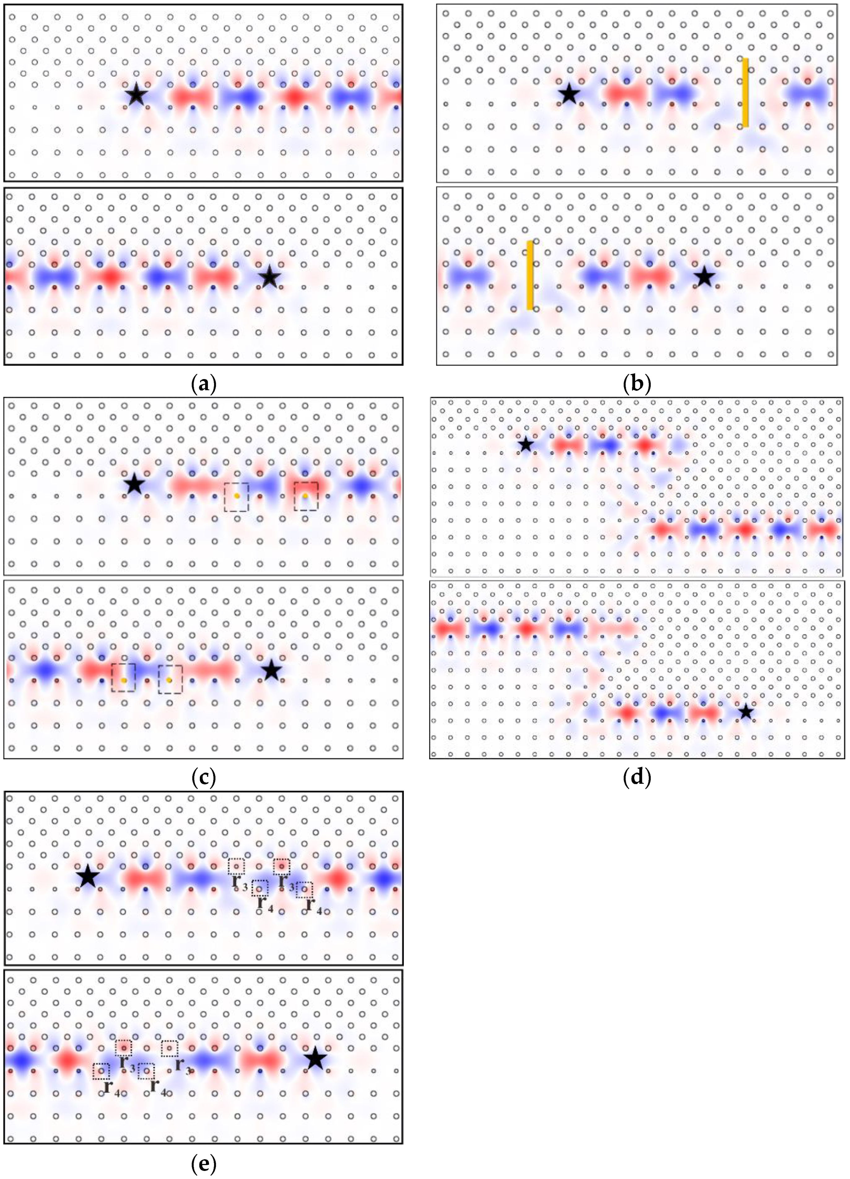
Figure 7.
The electric field distributions for at 4.2926 GHz in the unidirectional slow light PCW for parameters , (a) in the absence of the obstacles; (b) with an inserted metal reflector (indicated by the yellow rectangle); (c) with two YIG rods replaced by Copper rods (circled in the black rectangles) of the same size; (d) with a Z-shaped interface; (e) with rod defects (circled in the black rectangles and the corresponding rod radii are and respectively). The top and the bottom plots in (a–e) correspond to the results of the externally applied magnetic field along and direction, respectively. The point source is indicated by the black star. Blue and red colors represent negative and positive field strength values.

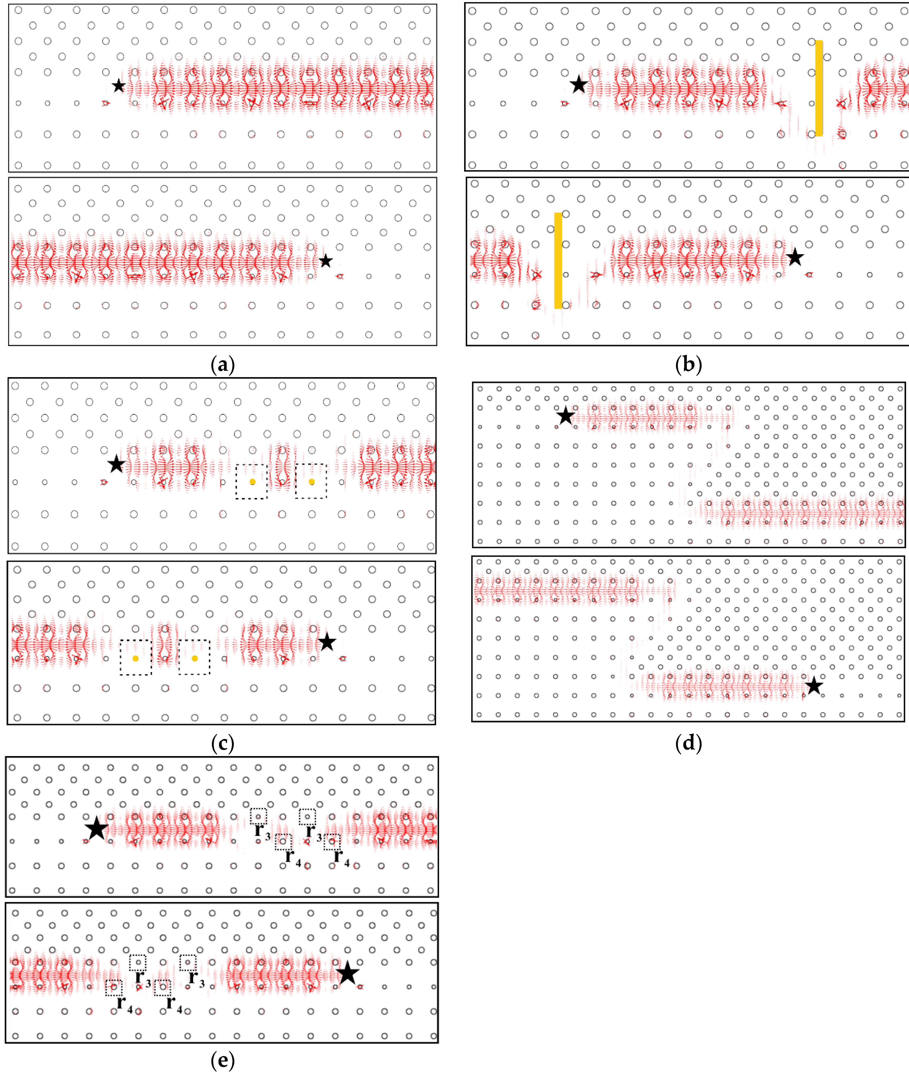
Figure 8.
The Poynting vectors distributions at 4.2926 GHz in the unidirectional slow light PCW for parameters , (a) in the absence of the obstacles; (b) with an inserted metal reflector (indicated by the yellow rectangle); (c) with two YIG rods replaced by Copper rods (circled in the black rectangles) of the same size; (d) with a Z-shaped interface; (e) with rod defects (circled in the black rectangles and the corresponding rod radii are and respectively). The top and the bottom plots in (a–e) correspond to the results of the externally applied magnetic field along and direction, respectively.


Table 1.
Group index, frequency bandwidth, and NDBP values under different optimized parameters and the comparison with previous works.
Table 1.
Group index, frequency bandwidth, and NDBP values under different optimized parameters and the comparison with previous works.
| Current Work | Optimized Parameters | Average Group Index | Frequency Bandwidth | NDBP Values |
| , | 77 | 0.444% | 0.342 | |
| , | 68 | 0.481% | 0.327 | |
| , | 64 | 0.485% | 0.311 | |
| , | 60 | 0.491% | 0.295 | |
| Previous Work | Modification of the Rod Radius | Average Group Index | Frequency Bandwidth | NDBP Values |
| Ref. [31] | 22.85 | 0.813% | 0.186 | |
| Ref. [46] | 26 | 0.896% | 0.233 | |
| Ref. [47] | 40 | 0.65% | 0.258 | |
| Ref. [48] | 62 | 0.43% | 0.268 |
© 2018 by the authors. Licensee MDPI, Basel, Switzerland. This article is an open access article distributed under the terms and conditions of the Creative Commons Attribution (CC BY) license (http://creativecommons.org/licenses/by/4.0/).
Share and Cite
MDPI and ACS Style
Zhang, Q.; Li, X. Unidirectional Slow Light Transmission in Heterostructure Photonic Crystal Waveguide. Appl. Sci. 2018, 8, 1858. https://doi.org/10.3390/app8101858
AMA Style
Zhang Q, Li X. Unidirectional Slow Light Transmission in Heterostructure Photonic Crystal Waveguide. Applied Sciences. 2018; 8(10):1858. https://doi.org/10.3390/app8101858
Chicago/Turabian StyleZhang, Qiuyue, and Xun Li. 2018. "Unidirectional Slow Light Transmission in Heterostructure Photonic Crystal Waveguide" Applied Sciences 8, no. 10: 1858. https://doi.org/10.3390/app8101858
Note that from the first issue of 2016, this journal uses article numbers instead of page numbers. See further details here.