Sub-Wavelength Scale Si Inverted Pyramid Fabrication with Enhanced Size Control by Using Silica Sphere Lithography Technique


1
Department of Materials Science and Engineering, Dong-A University, Saha-gu, Busan 604-714, Korea
2
School of Electrical, Computer and Energy Engineering, Arizona State University, Tempe, AZ 85287, USA
*
Author to whom correspondence should be addressed.
Appl. Sci. 2018, 8(10), 1720; https://doi.org/10.3390/app8101720
Submission received: 28 August 2018
/
Revised: 10 September 2018
/
Accepted: 19 September 2018
/
Published: 22 September 2018
(This article belongs to the Special Issue Next Generation Photovoltaic Solar Cells)
Abstract
:In this paper, we present a novel silicon (Si) subwavelength-scale surface structure (SWSS) fabrication process using the silica sphere (SS) lithography technique, which allows controllable geometries. The process involves a new cost-effective solvent-controlled spin-coating method that deposits SS on large Si surface areas with enhanced SS monolayer coverage and uniformity compared to conventional methods. The larger areas and rapid, low cost processing allow colloidal sphere lithography to be realistically used for solar cells. We successfully demonstrate 1.57 μm diameter SS on a 2-inch round Si wafer with more than 95% SS monolayer coverage and great uniformity. Using these deposited SS, a SWSS fabrication process was designed and successfully demonstrated Si inverted pyramid structures with dimension on the order of 1.1 μm, thus potentially providing a new technique for effective light-management of thin crystalline Si solar cells.
1. Introduction
Continued improvements in both solar cell cost and efficiency can be realized by continuing to decrease solar cell thickness. Reduced thickness has contributed to recent high efficiency and high voltage silicon (Si) solar cells, reaching over 750 mV open circuit voltage (VOC) on <100 micron thick wafers [1,2]. Further improvements in both optical control (light trapping) and reduced reflection leading to further efficiency enhancements require low-cost, controllable surface geometries. Previous reports have demonstrated that subwavelength-scale surface structures (SWSS) can offer an improved anti-reflection behavior over a broad wavelength range even at wide incident angles, resulting from the enhanced gradient in a refractive index in the structured layer [3]. Moreover, SWSS in an optimal scale and shape can also provide significant light path-length enhancement inside the Si absorber layer because of enhanced light trapping [4,5,6]. A recent report from Mavrokefalos, et al., demonstrated that an optimized subwavelength-scale inverted pyramid on a 10 μm thick c-Si absorber performs as a highly effective anti-reflection (AR) layer and achieves an improved absorption close to the Lambertian limit [7]. In addition to these optical advantages, thin Si PV enabled by SWSS can provide an enhanced open-circuit voltage (VOC) with improved photo-generated carrier collection [8]. However, despite the advantages of SWSS for thin c-Si PV, its commercial application is impractical using current fabrication techniques such as e-beam [9,10] and laser interference [11,12] lithography. These processes are time-consuming and relatively expensive and, as a result, are limited to research use and small cell areas. Therefore, a cost-effective and large area applicable SWSS fabrication process needs to be developed for the realization of future thin Si PV.
In this paper, we describe a novel SWSS fabrication process that enables the processing of Si inverted pyramid structures in a controlled scale on large Si surface areas. The Si surface patterning has been done with a silica sphere (SS) lithography technique to replace the conventional multi-step photolithography method. We have developed a solvent-controlled SS spin-coating method that enables deposition of a highly uniform SS monolayer on large surface areas [13]. Previous SS spin-coating methods based on water as a solvent require additional surfactant mixtures for (1) enhanced SS dispersion in solution, and (2) delayed solvent evaporation rate because of the properties of water [14]. Although surfactant addition offers significantly enhanced solution properties compared to pure water for uniform SS monolayer spin-coating; it is successful only for small area applications (e.g., 1-inch × 1-inch). Other conventional SS deposition methods including Langmuir–Blodgett coating and substrate surface functionalized spin-coating are not suitable for manufacturing due to their slowness and/or sensitivity to the processing environment [15,16,17]. To realize large area SS lithography with a simple and low-cost spin-coating approach, we use N,N-dimethyl-formamide (DMF) as a solvent and confirm that DMF can provide (1) a highly uniform close-packed SS monolayer with (2) minimal sensitivity to the spin-coating environment (e.g., vibration, humidity, and temperature), in addition to (3) large area SS deposition capability. Here, we demonstrate more than 95% SS monolayer coverage with outstanding uniformity on a 2-inch round Si wafer just with a simple spin-coating process performed in a non-environment controlled atmosphere.
One major advantage of SS lithography for SWSS fabrication is that SS offers highly flexible dimensional control of the structures. The period of fabricated structures can be easily changed by introducing different size of SS. In addition, the size of structure itself also can be adjusted by SS size reduction with dry etch process after SS spin-coating. In this work we utilized an optimized reactive-ion etching (RIE) condition designed mainly to etch the SS (i.e., SiO2) based on a CHF3 plasma assisted RIE process. We further demonstrate effective SWSS fabrication, especially, a well-arrayed inverted pyramid structure with dimension on the order of 1.1 μm and conclude that this will provide a more simplified and large-area applicable SWSS fabrication approach compared to conventional methods.
2. Experimental
Single side polished 2-inch diameter silicon wafers were used as substrates. Dry silica spheres (SS) sized at 1.57 μm were obtained from Bang Lab (10% possible size variation indicated by Bang Lab, Fishers, IN, USA). The common solvents (acetone and methanol) used in the experiment were purchased from Chemical Strategies, Inc. (Los Angeles, CA, USA). H2O2 (30 wt% in water) was purchased from Honeywell (Morris Plains, NJ, USA), H2SO4 (purity 96.0%) from KMG Chemicals, Inc. (Fort Worth, TX, USA), and N,N-dimethyl-formamide (DMF, Purity > 99%) from Sigma-Aldrich (Saint Louis, MO, USA).
Prior to SS spin-coating, the Si substrates were cleaned with acetone, methanol, and de-ionized (DI) water in that order, and submerged in a piranha solution (H2O2:H2SO4 = 1:4 volume ratio) for 15 min followed by a DI-water rinse and then dried in a spin rinse dryer at 1000 rpm for 10 min to provide clean and hydrophilic Si surfaces. The substrate when placed on the spin-coater is exposed to air under normal ambient laboratory conditions (Temperature: 20–23 °C, Humidity: 25–35%). The spin-coater was programmed with an acceleration speed of 100 rpm/s and maximum speed of 2000 rpm/s for 120 s. 300 μL of SS solution (630 mg/mL SS in DMF) was dispensed on the Si surface for spin-coating.
SS spin-coated Si were then moved to the reactive ion etching(RIE) chamber (Oxford PlasmaLab 80+) and the SS size reduction was performed using a CHF3/Ar mixed gases at 25/25 sccm flow rate with 200 Watts of RF plasma power under 75 mTorr chamber pressure. After RIE, ultra-violet ozone (UVO) surface cleaning treatment was followed to remove an organic passivating layer on the Si surface resulting from the CHF3/Ar RIE, and a Cr mask layer was deposited by using an e-beam evaporator (Lesker PVD-75). The SS layer on Si surface were then lift-off by dipping in a buffered oxide etch (10:1 BOE) solution for 10-min. The Cr masked Si substrate was then etched to fabricate inverted pyramids using a 1% KOH solution at 85°C with 4% iso-propanol (IPA) added to improve etching uniformity [18,19].
Scanning electron microscopy (SEM, FEI XL-30, Pillips, Amsterdam, The Netherlands) was used to observe the Si surface and the SEM image was investigated to calculate the coverage percentage of the SS monolayer by direct counting of the SS coated area through “Image J” (National Institutes of Health, Bethesda, MD, USA) image analysis software [20], which has been widely used for particle related surface analysis [21,22,23,24,25,26]. Then, the contact angle of solvent on a Si surface was also measured for wettability analysis by using the EasyDrop contact angle measurement system (KRUSS, Hamburg, Germany).
3. Results and Discussion
3.1. Deposition of Silica Sphere Monolayer
Prior to SWSS fabrication, deposition of a uniform and high coverage SS monolayer must be realized. We, therefore, developed a DMF solvent introduced spin-coating method which makes SS solution preparation easy and results in enhanced SS coverage and uniformity even on expanded Si surface areas [27]. Unlike conventional SS deposition techniques such as Langmuir–Blodgett (LB) dip-coating [15,16] and water-based spin-coating methods [21,28], our spin-coating process offers greatly reduced environmental sensitivity to, for example, vibration, humidity, and temperature along with reduced processing time. This is because DMF has more spin-coating oriented solvent properties compared to the conventional solvent, water. Figure 1 schematically compares the behavior of DMF and water during the various stages of spin-coating. First, from Figure 1b, DMF can provide outstanding wetting ability on a Si surface. From our contact angle measurements, the contact angle of DMF on a piranha cleaned Si surface was immeasurably small. This is an essential solvent property for fast, uniform, and omni-directional SS spread-out during spinning, which is also followed by less material loss due to its low centrifugal force caused by low surface tension at the liquid/solid interface, schematically shown in Figure 1d. Second, DMF also offers a significantly lower vapor pressure (VPDMF = 2.7 Torr at 20 °C) compared to that of water (VPwater = 17.54 Torr at 20 °C) providing increased SS deposition and distribution time during spin-coating due to its relatively slow evaporation rate, schematically illustrated in Figure 1f. This is also very important for spin-coating closely-packed SS assembly in a long range order (Figure 1h) since slower solvent evaporation produces intensified convective flux (Jw) of SS to the initially assembled SS (Figure 1f inset) [29]. However, water, due to its high vapor pressure (VP), requires humidity and temperature control or additional surfactant mixtures to delay the evaporation rate as previously reported [14,21]. Combining these two major advantages of DMF provides even less sensitivity to the spin-coating surface area, and we demonstrated more than 95% monolayer coverage even with much smaller SS (310 nm diameter) on a 2-inch round Si wafer, which is more challenging for spin-coating due to the stronger inter-particle interaction [13]. More details of DMF effect on SS spin-coating can be found in our previous study [27].
Figure 2 shows SEM images and a picture of a uniform spin-coated SS (1.57 μm diameter) monolayer on the Si surface with more than 95% coverage that has been achieved through the use of the DMF solvent without any modification of the surface [17] or spin-coating environment [21]. Therefore, with our novel solvent-controlled spin-coating method, we provide highly uniform and enhanced SS monolayer coverage even on large Si surface areas just by using a simple and low-cost spin-coating method.
3.2. Silica Sphere Size Control by RIE
One of the biggest advantages of utilizing SS for the nano-/micro-sphere lithography process is that silica material (i.e., SiO2) can provide high etching selectivity to other semiconductor materials, such as Si to adjust the scale of the surface structures. Currently, most reported nano-/micro-sphere lithography (NSL) processes utilize a polystyrene sphere (PS), which reveals a soft material nature that can be problematic to produce repeatable dimensions and well-defined patterns on the lithographic surface. In this report, we successfully demonstrated an enhanced SS size controllability with a RIE process and we believe that this can offer a great opportunity to fabricate SWSS in the desired dimensions.
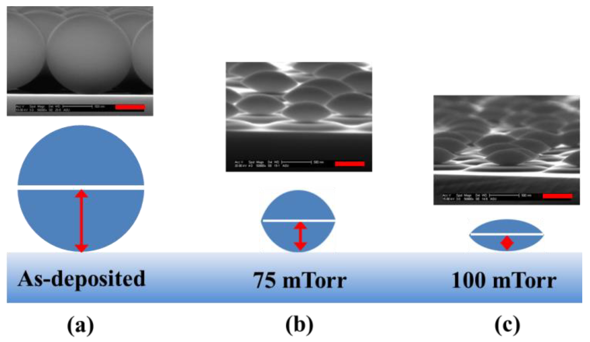
For effective size reduction of SS, two criteria are required. They are: (1) high etching selectivity of SS to Si substrate; and (2) effective horizontal direction etching of SS followed by minimized vertical etching. The high etching selectivity of SS to Si would prevent excess etching of Si surface, which is crucial to produce SWSS fabricated surface geometry in a desired way. In addition, well-controlled horizontal direction etching of SS is required to adjust the dimension of a projected pattern after mask layer deposition, but vertical direction etching must be minimized to permit clean SS removal and mask layer lift-off. Based on these considerations, a CHF3/Ar gas mixture is used for the SS etching process and has optimized its etching conditions by changing gas flow rates, RF power, and chamber pressure. After the investigation of each RIE result, we found that the chamber pressure is the most critical knob to produce high SS etching selectivity and a low vertical/horizontal etching ratio. For the experiments, three different chamber pressures were studied, which are 50, 75, and 100 mTorr, and the results are shown in Table 1. From Table 1, we observed that noticeable Si substrate etching was made after etching at 50 mTorr, but as chamber pressure increases to 75 and 100 mTorr, the Si substrate etching was significantly reduced, which is possibly due to the decreased mean-free path length of ionized-species at higher pressure [30]. However, even though significantly reduced Si substrate etching was observed for both pressures of 75 and 100 mTorr, 100 mTorr revealed a higher vertical/horizontal etching ratio of 3.9 compared to 2.6 from 75 mTorr. As mentioned in the earlier section, this excess etching rate in the vertical direction is not ideal for SS lithography because fast vertical diameter reduction of SS compared to that of the horizontal direction restricts our choice on the pattern sizes, which weaken the ability of the SS to pattern the surface as SS size decreases. As shown in Figure 3, for the same SS target horizontal diameter, 800 nm, 100 mTorr chamber pressure produced a reduced vertical SS diameter of 260 nm, compared to 360 nm from 75 mTorr, while the horizontal diameters were sustained at 800 nm for both. Therefore, we decided to use 75 mTorr chamber pressure for SS size reduction with RIE.
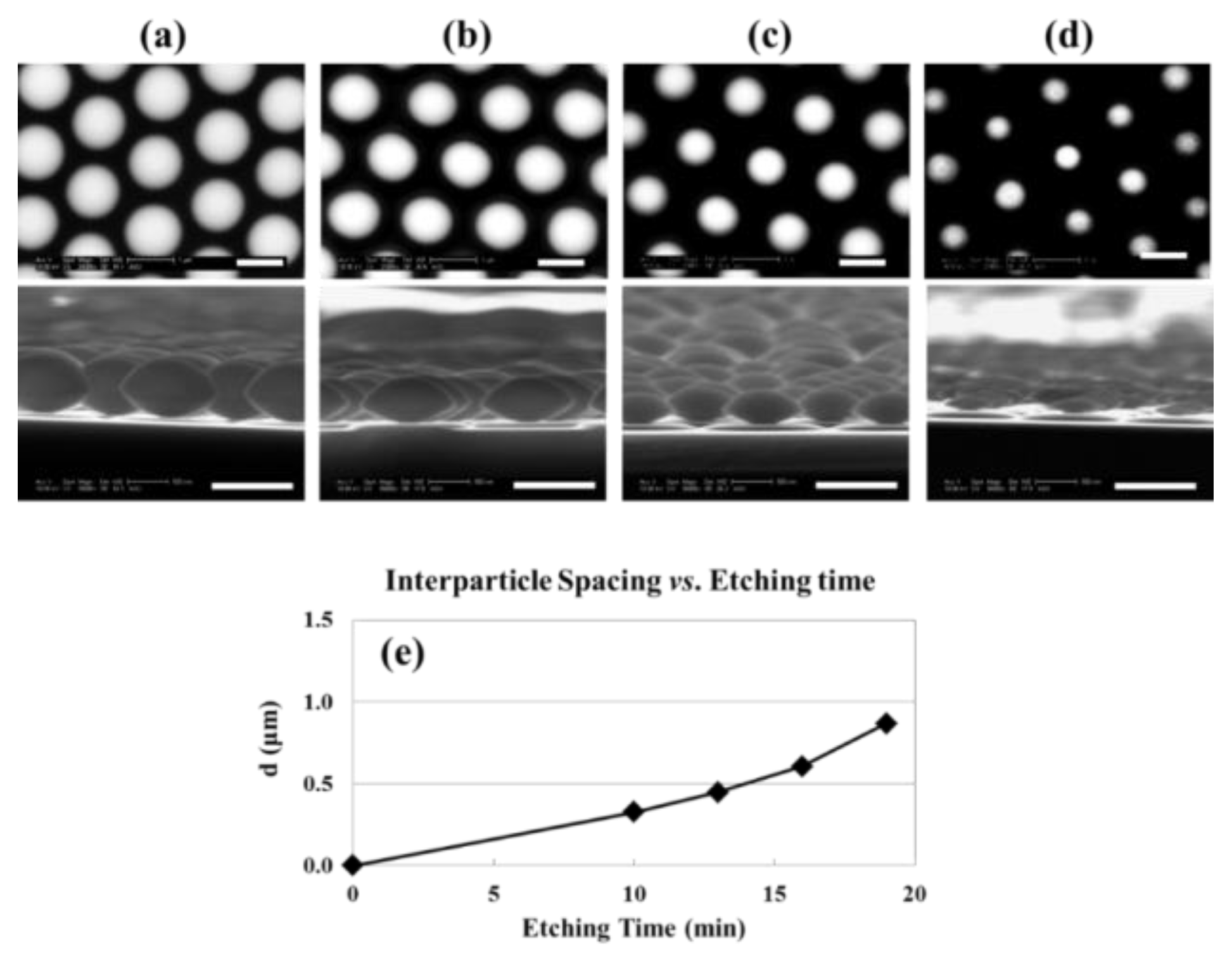
In Figure 4, we show 1.57 μm diameter SS after different RIE process times (10-min, 13-min, 16-min, 19-min) under our optimized RIE condition. From Figure 4a–d, we confirmed that highly effective SS size reduction is possible with minimal Si substrate etching. In addition, from Figure 4e, the measured inter-particle spacing with different etching times reveals that SS size can be easily reduced in a desired scale due to its reasonably linear relation between decreased SS diameter and etching time. Moreover, as we observed from Figure 4a–d, after RIE, there was still highly well-defined circle shape of SS without any rugged shape at the edge, which is a well-known issue with a soft polystyrene sphere [31,32]. Therefore, by using our optimal RIE condition, highly controlled SWSS in an intended structure dimension and period by introducing SS in a different diameter.
3.3. Mask Layer Deposition and SS Removal
In the earlier sections, we demonstrated that CHF3/Ar RIE could provide very effective selective etching of SS to the Si substrate and well controlled SS size reduction. CHF3/Ar RIE process, however, also convey an inevitable issue for SS layer elimination after metal mask layer deposition. The challenge of this SS layer removal has been originated from the thin SiCxFy layer formation on the all exposed surfaces during RIE [33]. This carbon included SiCxFy compound layer is very stable, especially in a hydrofluoric acid (HF) based solution like BOE. As a consequence, removal of SiCxFy covered SS in BOE solution cannot be achieved. The SiCxFy layer effect for SS removal from Si surface is schematically shown in Figure 5c,e. As illustrated in Figure 5e with an actual SEM image, the presence of SiCxFy layer on the surface of SS resulted in a collapsed Cr metal mask layer during the BOE process and no surface patterning for surface structure fabrication. This is because the SiCxFy is stable in BOE, but SS itself was etched away by infiltrated BOE. To solve the issue of SiCxFy layer, therefore, we inserted an ultra-violet ozone (UVO) surface cleaning treatment, which is simple and required a no-vacuum process. This UVO treatment was performed before the Cr layer deposition. The UVO process provides not only effective cleaning on organic contamination, but also a non-aggressive etching environment to prevent possible surface damage inducing degraded solar cell performance. The effect of UVO surface treatment is clearly shown in Figure 5f. For the sample, a 10-min UVO treatment was performed before Cr layer evaporation, and as expected, the surface revealed very clean SS removal after BOE (10:1) etch, resulting in well-defined surface patterns for SWSS fabrication.
3.4. SWSS Fabrication: Inverted Pyramid
For the first demonstration of SWSS from our designed lithography process, we decided to fabricate an inverted pyramid Si surface structure which is well known for its highly effective light trapping when it is built in an optimal subwavelength scale [7]. In this paper, we successfully demonstrated the effectiveness of our lithography process and the results are shown in Figure 6. With our process, we fabricated a ~1.1 μm scale inverted pyramid with ~1.57 μm period in a hexagonal array. (Note: Optically, this is not an optimal SWSS scale and density, but is intended to show the capability to control the size and density of fabricated SWSS.) To provide a stable masking layer on the Si surface for the KOH etching process, Cr metal layer has been chosen since it provides a reasonably robust material nature in both BOE and KOH solutions. In addition, Cr is a relatively cheap material that meets our intention to develop a low cost lithography process in this article. For Cr mask layer deposition, an e-beam evaporation system has been used and deposited a 50 nm thick Cr layer. The sample with Cr layer was, then, dipped in BOE (10:1) solution for SS layer etch. The SS removed Si sample was subsequently immersed in KOH (1%) solution for anisotropic etching of Si inverted pyramid structure. The KOH solution was prepared after Si saturation and 4% IPA addition to provide moderate Si etching rate and enhanced etching uniformity for fabricated structures. After 2-min KOH etching at 85 °C, well dimension-defined Si inverted pyramids were produced as shown in Figure 6b–d. In Figure 6a, the diameter of patterned circle was ~1.1 μm, and the lateral dimension of fabricated Si inverted pyramid is also approximately 1.1 μm, as shown in Figure 6b. Furthermore, we also successfully confirmed that our SWSS fabrication process using a solvent-controlled SS lithography technique can produce highly uniform Si inverted pyramid over a large surface area in a desired dimension and density as shown in Figure 6c–e. In the study from Mavrokefalos et al., the optimized dimension of SWSS can produce a greatly enhanced absorption close to the Lambertian limit in the visible and near IR regions [7]. Therefore, future dimension and period optimization for SWSS will be able to produce broadband absorption enhancement for thin c-Si solar cell applications.
4. Conclusions
In this paper, a novel SS based lithography technique using a solvent-controlled spin-coating method has successfully demonstrated to deposit a uniform SS monolayer on large Si surfaces. Based on our SS deposition method, we designed a SWSS fabrication process targeting 1.1 μm inverted Si pyramid surface structures with 1.57 μm period in a hexagonal array. We successfully demonstrated that our process can provide a promising approach to fabricate SWSS in controlled-scale even on a relatively large Si surface areas. Furthermore, from the results, we showed that our process offers great flexibility in varying the target size and density of the SWSS by using a simple RIE process and different size SS. Therefore, our process potentially provides a more realistic approach for surface texturing of thin c-Si PV cells with broadband absorption improvement. Currently, we are working on optical modeling to determine the optimal size of SWSS for enhanced light absorption for thin c-Si solar cell application, and the results will be reported shortly.
Author Contributions
Reviewed and Editing, C.B.H.; Read and Approved, J.-Y.C. and C.B.H.; Guided the Research, C.B.H.
Funding
This work was supported by the Dong-A University research fund.
Conflicts of Interest
The authors declare no conflict of interest.
References
- Herasimenka, S.Y.; Dauksher, W.J.; Bowden, S.G. >750 mV open circuit voltage measured on 50 μm thick silicon heterojunction solar cell. Appl. Phys. Lett. 2013, 103, 053511. [Google Scholar] [CrossRef]
- Taguchi, M.; Yano, A.; Tohoda, S.; Matsuyama, K.; Nakamura, Y.; Nishiwaki, T.; Fujita, K.; Maruyama, E. 24.7% Record Efficiency HIT Solar Cell on Thin Silicon Wafer. IEEE J. Photovolt. 2014, 44, 96–99. [Google Scholar] [CrossRef]
- Tian, B.; Zheng, X.; Kempa, T.J.; Fang, Y.; Yu, N.; Yu, G.; Huang, J.; Lieber, C.M. Coaxial silicon nanowires as solar cells and nanoelectronic power sources. Nature 2007, 449, 885–889. [Google Scholar] [CrossRef] [PubMed]
- Chutinan, A.; John, S. Light trapping and absorption optimization in certain thin-film photonic crystal architectures. Phys. Rev. A 2008, 78, 023825. [Google Scholar] [CrossRef]
- Tobias, I.; Luque, A.; Marti, A. Light intensity enhancement by diffracting structures in solar cells. J. Appl. Phys. 2008, 104, 034502. [Google Scholar] [CrossRef] [Green Version]
- Lin, C.; Povinelli, M.L. Optical absorption enhancement in silicon nanowire arrays with a large lattice constant for photovoltaic applications. Opt. Express 2009, 17, 19371–19381. [Google Scholar] [CrossRef] [PubMed]
- Mavrokefalos, A.; Han, S.E.; Yerci, S.; Branham, M.S.; Chen, G. Efficient Light Trapping in Inverted Nanopyramid Thin Crystalline Silicon Membranes for Solar Cell Applications. Nano Lett. 2012, 12, 2792–2796. [Google Scholar] [CrossRef] [PubMed]
- Jeong, S.; McGehee, M.D.; Cui, Y. All-back-contact ultra-thin silicon nanocone solar cells with 13.7% power conversion efficiency. Nat. Commun. 2013, 4, 2950. [Google Scholar] [CrossRef] [PubMed] [Green Version]
- Juhasz, R.; Elfstrom, N.; Linnros, J. Controlled fabrication of silicon nanowires by electron beam lithography and electrochemical size reduction. Nano Lett. 2005, 55, 275–280. [Google Scholar] [CrossRef] [PubMed]
- Zhang, J.; Shokouhi, B.; Cui, B. Tilted nanostructure fabrication by electron beam lithography. J. Vac. Sci. Technol. B 2012, 30, 06F302. [Google Scholar] [CrossRef]
- Ertorer, E.; Vasefi, F.; Keshwah, J.; Najiminaini, M.; Halfpap, C.; Langbein, U.; Carson, J.J.L.; Hamilton, D.W.; Mittler, S. Large area periodic, systematically changing, multishape nanostructures by laser interference lithography and cell response to these topographies. J. Biomed. Opt. 2013, 18, 035002. [Google Scholar] [CrossRef] [PubMed] [Green Version]
- Tan, C.; Peng, C.S.; Pakarinen, J.; Pessa, M.; Petryakov, V.N.; Verevkin, Y.K.; Zhang, J.; Wang, Z.; Olaizola, S.M.; Berthou, T. Ordered nanostructures written directly by laser interference. Nanotechnology 2009, 20, 12. [Google Scholar] [CrossRef] [PubMed]
- Choi, J.Y.; Honsberg, C.B. Reactive Ion Etching Surface Texturing of c-Si using Silica Nanosphere lithography technique for Solar Cell Application. Presented at 2013 IEEE 39th Photovoltaic Specialists Conference, Tampa, FL, USA, 16–21 June 2013. [Google Scholar]
- Mihi, A.; Ocana, M.; Miguez, H. Oriented colloidal-crystal thin films by spin-coating microspheres dispersed in volatile media. Adv. Mater. 2006, 18, 2244–2249. [Google Scholar] [CrossRef]
- Huang, J.X.; Kim, F.; Tao, A.R.; Connor, S.; Yang, P. Spontaneous formation of nanoparticle stripe patterns through dewetting. Nat. Mater. 2005, 44, 896–900. [Google Scholar] [CrossRef] [PubMed]
- Hsu, C.M.; Connor, S.T.; Tang, M.X.; Cui, Y. Wafer-scale silicon nanopillars and nanocones by Langmuir-Blodgett assembly and etching. Appl. Phys. Lett. 2008, 93, 133109. [Google Scholar] [CrossRef]
- Jiang, P.; Prasad, T.; McFarland, M.J.; Colvin, V.L. Two-dimensional nonclose-packed colloidal crystals formed by spincoating. Appl. Phys. Lett. 2006, 89, 011908. [Google Scholar] [CrossRef]
- Cho, W.J.; Chin, W.K.; Kuo, C.T. Effects of alcoholic moderators on anisotropic etching of silicon in aqueous potassium hydroxide solutions. Sens. Actuators A 2004, 116, 357–368. [Google Scholar] [CrossRef]
- Zubel, I. Silicon anisotropic etching in alkaline solutions III: On the possibility of spatial structures forming in the course of Si(100) anisotropic etching in KOH and KOH plus IPA solutions. Sens. Actuators A 2000, 84, 116–125. [Google Scholar] [CrossRef]
- Rasband, W. Imagej; U.S. National Institutes of Health: Bethesda, MD, USA, 1997–2006. Available online: https://imagej.nih.gov/ij/ (accessed on 1 August 2018).
- Ogi, T.; Modesto-Lopez, L.B.; Iskandara, F.; Okuyama, K. Fabrication of a large area monolayer of silica particles on a sapphire substrate by a spin coating method. Colloids Surf. A 2007, 297, 71–78. [Google Scholar] [CrossRef]
- Rykaczewski, K.; Hildreth, O.J.; Wong, C.P.; Fedorov, A.G.; Scott, J.H.J. Guided Three-Dimensional Catalyst Folding during Metal-Assisted Chemical Etching of Silicon. Nano Lett. 2011, 11, 2369–2374. [Google Scholar] [CrossRef] [PubMed]
- Zhang, L.; Qiao, S.Z.; Jin, Y.G.; Chen, Z.G.; Gu, H.C.; Lu, G.Q. Magnetic hollow spheres of periodic mesoporous organosilica and Fe3O4 nanocrystals: Fabrication and structure control. Adv. Mater. 2008, 20, 805–809. [Google Scholar] [CrossRef]
- Izak-Nau, E.; Voetz, M.; Eiden, S.; Duschl, A.; Puntes, V.F. Altered characteristics of silica nanoparticles in bovine and human serum: The importance of nanomaterial characterization prior to its toxicological evaluation. Part. Fibre Toxicol. 2013, 10, 56. [Google Scholar] [CrossRef] [PubMed]
- Wan, Q.; Ramsey, C.; Baran, G. Thermal pretreatment of silica composite filler materials. J. Therm. Anal. Calorim. 2010, 99, 237–243. [Google Scholar] [CrossRef] [PubMed]
- Schneider, C.A.; Rasband, W.S.; Eliceiri, K.W. NIH Image to ImageJ: 25 years of image analysis. Nat. Methods 2012, 99, 671–675. [Google Scholar] [CrossRef]
- Choi, J.-Y.; Alford, T.L.; Honsberg, C.B. Solvent-Controlled Spin-Coating Method for Large-Scale Area Deposition of Two-Dimensional Silica Nanosphere Assembled Layers. Langmuir 2014, 30, 5732–5738. [Google Scholar] [CrossRef] [PubMed]
- Hulteen, J.C.; Vanduyne, R.P. Nanosphere lithography: A materials general fabrication process for periodic particle array surfaces. J. Vac. Sci. Technol. A 1995, 13, 1553–1558. [Google Scholar] [CrossRef]
- Denkov, N.; Velev, O.; Kralchevski, P.; Ivanov, I.; Yoshimura, H.; Nagayama, K. Mechanism of formation of two-dimensional crystals from latex particles on substrates. Langmuir 1992, 88, 3183–3190. [Google Scholar] [CrossRef]
- Jansen, H.; Gardeniers, H.; de Boer, M.; Elwenspoek, M.; Fluitman, J. A survey on the reactive ion etching of silicon in microtechnology. J. Micromech. Microeng. 1996, 66, 14–28. [Google Scholar] [CrossRef]
- Cheung, C.L.; Nikolić, R.J.; Reinhardt, C.E.; Wang, T.F. Fabrication of nanopillars by nanosphere lithography. Nanotechnology 2006, 17, 1339–1343. [Google Scholar] [CrossRef] [Green Version]
- Oh, N.R.; Song, T.J.; Lim, S.K.; Yoon, C.S. Polystyrene Nanosphere Lithography Improved by the Insertion of a Sacrificial Polyimide Film. Electron. Mater. Lett. 2005, 11, 135–139. [Google Scholar]
- Easwarakhanthana, T.; Beyssen, D.; Le Brizoual, L.; Bougdira, J. Spectroellipsometric analysis of CHF3 plasma-polymerized fluorocarbon films. J. Vac. Sci. Technol. A 2006, 24, 1036–1043. [Google Scholar] [CrossRef]
Figure 1.
Schematic illustration to compare N,N-dimethyl-formamide (DMF) and water for spin-coating application.
Figure 1.
Schematic illustration to compare N,N-dimethyl-formamide (DMF) and water for spin-coating application.

Figure 2.
(a) Picture of silica sphere (SS) coated Si wafer (2-inch diameter) and (b) scanning electron microscope (SEM) images of SS coated Si surface.
Figure 2.
(a) Picture of silica sphere (SS) coated Si wafer (2-inch diameter) and (b) scanning electron microscope (SEM) images of SS coated Si surface.

Figure 3.
SEM images of SS (a) as-deposited, and after reactive-ion etching (RIE) process at (b) 75 mTorr, and (c) 100 mTorr.
Figure 3.
SEM images of SS (a) as-deposited, and after reactive-ion etching (RIE) process at (b) 75 mTorr, and (c) 100 mTorr.

Figure 4.
SEM images of RIE processed SS after different etching time (a) 10 min, (b) 13 min, (c) 16 min, and (d) 19 min, (e) graph indicating inter-particle spacing with etching time (All samples were etched at the same RIE condition which are 75 mTorr pressure, 200 Watts RF power, and 25/25 sccm gas flow rate except etching time) (scale bar:1 μm).

Figure 5.
(a–f) Schematic illustration of ultra-violet ozone (UVO) treatment effect on SS removal after RIE. (Green-line indicates deposited Cr layer, and red-line for SiCxFy passivating layer formed during RIE process, scale-bar = 1 μm).
Figure 5.
(a–f) Schematic illustration of ultra-violet ozone (UVO) treatment effect on SS removal after RIE. (Green-line indicates deposited Cr layer, and red-line for SiCxFy passivating layer formed during RIE process, scale-bar = 1 μm).

Figure 6.
SEM images of (a) SS removed Cr mask layer deposited Si surface, (b) 1% KOH etched Si surface with Cr mask layer, (c) inverted Si pyramid without Cr mask layer, (d) cross-sectional image of inverted Si pyramid, and (e) fabricated inverted pyramids over large surface area to show its uniformity (Inverted pyramid has ~10% size variation likely caused by an initial SS size variation of 10%.). Note: (a–d) scale-bar = 1 μm, and (e) scale-bar = 10 μm.


Table 1.
SS shape profile change with CHF3/Ar gas RIE after 10-min etching under three different chamber pressures.
Table 1.
SS shape profile change with CHF3/Ar gas RIE after 10-min etching under three different chamber pressures.
| PressureProperty | 50 mTorr | 75 mTorr | 100 mTorr |
|---|---|---|---|
| Cross-sectional SEM Image (Scale-bar:500 nm) |  |  |  |
| Vertical Etching Rate (nm/min) | 90.3 | 80.3 | 70.3 |
| Horizontal Etching Rate (nm/min) | 34.8 | 30.3 | 18.1 |
| Vertical/Horizontal Etching Ratio | 2.6 | 2.6 | 3.9 |
© 2018 by the authors. Licensee MDPI, Basel, Switzerland. This article is an open access article distributed under the terms and conditions of the Creative Commons Attribution (CC BY) license (http://creativecommons.org/licenses/by/4.0/).
Share and Cite
MDPI and ACS Style
Choi, J.-Y.; Honsberg, C.B. Sub-Wavelength Scale Si Inverted Pyramid Fabrication with Enhanced Size Control by Using Silica Sphere Lithography Technique. Appl. Sci. 2018, 8, 1720. https://doi.org/10.3390/app8101720
AMA Style
Choi J-Y, Honsberg CB. Sub-Wavelength Scale Si Inverted Pyramid Fabrication with Enhanced Size Control by Using Silica Sphere Lithography Technique. Applied Sciences. 2018; 8(10):1720. https://doi.org/10.3390/app8101720
Chicago/Turabian StyleChoi, Jea-Young, and Christiana B. Honsberg. 2018. "Sub-Wavelength Scale Si Inverted Pyramid Fabrication with Enhanced Size Control by Using Silica Sphere Lithography Technique" Applied Sciences 8, no. 10: 1720. https://doi.org/10.3390/app8101720
Note that from the first issue of 2016, this journal uses article numbers instead of page numbers. See further details here.