Review

Eliminating Light-Induced Degradation in Commercial p-Type Czochralski Silicon Solar Cells

1
School of Photovoltaic and Renewable Energy Engineering, University of New South Wales, Sydney, NSW 2052, Australia
2
Department of Physics, University of Konstanz, Universitätsstr. 10, 78457 Konstanz, Germany
3
Now with Department of Materials, University of Oxford, 16 Parks Rd, Oxford OX1 3PH, UK
4
Now with Department of Electronics and Nanoengineering, Aalto University, Tiototie 3, 02150 Espoo, Finland
*
Author to whom correspondence should be addressed.
These authors contributed equally to this manuscript.
Appl. Sci. 2018, 8(1), 10; https://doi.org/10.3390/app8010010
Submission received: 23 November 2017 / Revised: 14 December 2017 / Accepted: 18 December 2017 / Published: 22 December 2017
(This article belongs to the Special Issue Next Generation Photovoltaic Solar Cells)

Abstract

:
This paper discusses developments in the mitigation of light-induced degradation caused by boron-oxygen defects in boron-doped Czochralski grown silicon. Particular attention is paid to the fabrication of industrial silicon solar cells with treatments for sensitive materials using illuminated annealing. It highlights the importance and desirability of using hydrogen-containing dielectric layers and a subsequent firing process to inject hydrogen throughout the bulk of the silicon solar cell and subsequent illuminated annealing processes for the formation of the boron-oxygen defects and simultaneously manipulate the charge states of hydrogen to enable defect passivation. For the photovoltaic industry with a current capacity of approximately 100 GW peak, the mitigation of boron-oxygen related light-induced degradation is a necessity to use cost-effective B-doped silicon while benefitting from the high-efficiency potential of new solar cell concepts.

1. Introduction

One of the most significant challenges for humanity is the need to shift away from using fossil fuel technologies for electricity generation and transportation needs with a transition towards the use of renewable resources. Without additional efforts to reduce greenhouse gas emissions beyond those already in place today, the projected emissions growth, driven by continued population and economic growth, is expected to result in an average increase of an alarming 3.7–4.8 °C by 2100, compared to pre-industrial levels [1]. Such increases in atmospheric CO2 levels could lead to dramatic changes in the thermohaline circulation patterns that regulate the world’s climate, with severe consequences for marine and terrestrial ecosystems [2]. As a result, significant cuts to anthropogenic greenhouse gas emissions are required by 2050 to avoid these dramatic changes. One promising approach to reduce greenhouse gas emissions is through the widespread adoption of photovoltaics (PV) for electricity generation. The PV industry is rapidly growing, with astonishing growth rates of 30–50% per annum since the 1990’s [3,4], alongside significant reductions in cost [5]. In 2016, approximately 75 GW peak (GWp) of PV power was installed, taking the cumulative installed PV capacity to >300 GWp [5].
One of the primary drivers for the increased uptake of PV is through the cost reductions achieved by improving the efficiency of the PV modules. However, approximately 95% of PV modules are fabricated using p-type silicon substrates [5], which are prone to degradation when exposed to sunlight [6,7], even at temperatures as low as 70 °C encountered under typical working conditions of solar panels. In p-type Czochralski (Cz) grown silicon, such light-induced degradation (LID) has plagued the industry for decades and has been a driver for intense research into alternative silicon materials for PV production. This degradation is believed to be due to the formation of boron-oxygen (B-O) related defects [8], although the actual composition of the defect is still unclear and remains a contentious issue [9,10,11]. A thorough review of B-O defects by Niewelt et al. can be found in [12].
B-O related degradation can reduce the 1-sun standard test conditions (STC) efficiency of silicon solar cells by up to 10% relative to the performance immediately after cell production [13]. However, in practice it is much smaller than this, typically plateauing at a value of 3–4%relative for conventional aluminium back-surface-field (Al-BSF) solar cells [14] and 4–6%relative for the passivated emitter, rear cell (PERC) structure [15]. Furthermore, this performance change is transient with an initial degradation cycle followed by a natural recovery back to the starting performance. The net impact on the total energy yield of an affected module depends on many factors and can last days, weeks, months or even years depending on the installation location and type [16]. This performance instability has created uncertainty in the minds of large-scale installers who from a bankability perspective prefer the issue be mitigated during manufacturing. With a prediction of 100 GW of global PV module sales in 2017 [17], B-O related degradation of p-type Cz solar cells could cost solar cell manufacturers $390 M for the year. This valuation is based on a 2016 market share of 20.5% (4.4%) for p-type Cz Al-BSF (PERC) modules [18] with a degradation of 4%relative (6%relative) and selling price of US 0.35 $/W (0.40 $/W) (12 December 2017) [19].
Despite the uncertainties surrounding the nature of the defect, significant progress has been made over the last ten years for the elimination of B-O related LID. This paper will review the progress in the understanding of B-O LID mitigation processes and the impact on the industry. In particular, B-O related LID will be discussed in relation to the development new illuminated annealing processes to treat affected material and the incorporation of such processes into industrial solar cell fabrication.

2. Alternative Silicon Materials to Avoid Boron-Oxygen (B-O) Light-Induced Degradation (LID)

Fundamentally, B-O related LID occurs in industrial p-type Cz silicon solar cells due to the simultaneous presence of boron and interstitial oxygen (Oi) in the silicon wafer. Some studies have investigated the impact of the concentration of both boron and Oi on the extent of B-O LID. The recombination rate from B-O defects is often used to provide a quantitative estimation of the defect concentration, denoted as the normalised defect density (NBO*) [20]. The NBO* is strongly dependent on the interstitial oxygen concentration ([Oi]) [21], scaling approximately quadratically with [Oi] [8,22,23,24]. A strong dependence of NBO* on the boron doping concentration has also been observed. For the most common Cz wafers used in the industry [5], doped solely with boron, the NBO* scales approximately linearly with the boron doping concentration [20,22,23,25,26]. This boron-doping dependence is also the case for p-type Cz wafers co-doped with boron and gallium [27]. Even phosphorous-doped n-type Cz-Si partially compensated with boron shows B-O LID, although in that case, the kinetics differ, most probably due to the fundamentally different background conditions (carrier concentrations, Fermi level position etc.) [28,29,30]. For further details, see Ref. [12].
For p-type Cz wafers doped solely with boron, an empirical model of the stable carrier lifetime after the formation of B-O defects was presented in early work. This work established a reduction in carrier lifetime scaling approximately linearly with increasing boron concentration and quadratically with increasing [Oi] [23]. Subsequently, one option to avoid B-O related LID is to modify the source material used to make the solar cells. In particular, a reduction in the extent of B-O LID can be achieved by reducing either the boron or Oi concentration in the silicon material.

2.1. Decreasing the Interstitial Oxygen Concentration

A negative side effect of Cz growing technique is a quite strong level of oxygen contamination. Silicon feedstock is melted in a quartz (SiO2) crucible from which the crystal is pulled with rather low growth rates. As molten silicon is highly reactive, it partially dissolves the crucible during growth thus continuously enriching the melt with oxygen, which then is incorporated unintentionally into the growing crystal.
Several alternative crystallisation approaches exist that can reduce the interstitial oxygen concentration in silicon wafers. When using mono-crystalline silicon one approach to reduce the [Oi] is to use Float-zoned (FZ) silicon. FZ silicon typically has an [Oi] two orders of magnitude lower than that in Cz material [31], which suppresses B-O related LID [21]. However, FZ silicon wafers are significantly more expensive than those produced from Cz silicon and hence not preferred by solar cell manufacturers. FZ silicon can also be subject to various other defects, such as nitrogen related defects or LID effects that can significantly reduce bulk lifetimes [32,33,34].
For Cz silicon, [Oi] may be reduced by applying magnetic fields during crystal growth, manipulating convective flows in the melt [35,36]. However, this technique has proven challenging for the current size of industrial Cz ingots and throughput/cost constraints for solar cell fabrication. Alternatively, coatings such as silicon nitride can be used on the wall of the crucible [37] to reduce [Oi] by up to one order of magnitude [38,39]. This method is commonly used by the industry. Control of the crystallisation parameters such as crucible and crystal rotation, pressure and ambient atmosphere can also reduce [Oi] [37].
Alternatively, casting methods can be used to reduce the [Oi] in the silicon wafers [40]. However, the casting method results in multi-crystalline crystal growth with large structural defects such as dislocation clusters and grain boundaries. Also, a range of contaminants is often introduced into the silicon ingot that typically originates from less pure crucible material. Both structural defects and contaminations reduce carrier lifetime [41,42] and thus solar cell efficiency, especially when a cell architecture like PERC (passivated emitter and rear cell) is used which benefits from high carrier lifetimes. BP Solar developed a promising casting approach to eliminate grain boundaries by seeding the growth of mono-crystalline silicon [43]. Unfortunately, this material suffers from significant quality variations throughout the ingot due to the generation of high dislocation densities [44] and unintended partial multi-crystalline crystal growth. As a result, the industry has not adopted this approach to date [45]. An alternative casting method seeds the crystal growth to deliberately reduce the grain size, therefore reducing dislocation densities, to produce “high-performance multi” [46]. This material is rapidly being adopted by the industry to replace conventional cast silicon material [5]. However, these wafers suffer from a different form of degradation that can reduce cell performance by as much as 12%relative [7,47,48,49,50], which has posed a significant challenge for solar cell manufacturers with the transition to the PERC cell technology [5]. In general, while cast silicon material is cheaper than Cz silicon and less susceptible to B-O LID, the casting methods introduce more severe recombination mechanisms into the silicon bulk. At the end of 2017 (6 December) wafer prices were US$0.629 for high-performance multi-crystalline silicon and US$0.716 for mono-crystalline silicon and Al-BSF cell prices were US$0.894 for multi-crystalline silicon and US$1.005 for mono-crystalline silicon [19]. Assuming identical processing costs per cell, US$0.024 will be lost for each cell by solar cell manufacturers by fabricating multi-crystalline silicon wafers. This loss equates to US$500 M for the year assuming an annual capacity of 100 GW and 4.8 W per mono-crystalline cell.

2.2. Decreasing the Boron Doping Concentration

Another alternative to fabricating wafers that are less susceptible to B-O LID is the use of wafers with reduced boron doping concentration and hence higher bulk resistivity. Decreasing the boron doping concentration not only reduces the concentration of B-O defects but has the added benefit of reducing the sensitivity to Shockley-Read-Hall (SRH) recombination [51,52]. However, for PERC solar cells, this increases bulk resistance in the device for the lateral flow of majority carriers to the localised p-type contacts. Hence, there is a trade-off between reducing the effects of reducing SRH recombination in general and B-O LID in particular and increasing series resistance within the bulk. As a result, mid-range doping around 2–5 Ωcm is mostly used in industrial applications.
Boron can also be substituted with other dopants. If retaining a p-type substrate, typically gallium is used. The benefit of using gallium-doped wafers is that they are free of any B-O related LID effects. However, like boron-doped wafers, they are susceptible to the formation of acceptor-iron pairs [53,54]. A weakness of gallium-doped ingots is the substantially lower segregation coefficient for gallium (8 × 10⁻³) than that for boron (0.8) [55,56]. The low segregation coefficient results in a large range of wafer resistivities throughout a Cz ingot that can lead to significant variations in the electrical parameters and potentially reduce the usable portion of the ingot. Other p-type dopants such as aluminium or indium can also be used. The drawback is that these have even smaller segregation coefficients than gallium of 2 × 10⁻³ and 4 × 10⁻⁴, respectively [55,56]. Furthermore, aluminium is susceptible to the formation of recombination active defects with Oi [57] and indium doped Cz wafers are also susceptible to LID [58].
Phosphorus-doped n-type wafers can also be used to eliminate B-O defects, provided that the material is not compensated with boron dopants [25]. Two strengths of n-type wafers are that they are less susceptible to intrinsic recombination [59] as well as to SRH recombination from impurities such as iron [60]. Besides, for a given resistivity, n-type wafers have a lower dark saturation current than their p-type counterparts. As a result, n-type wafers have higher lifetimes than p-type wafers. On the other hand, n-type wafers are more susceptible to SRH recombination from other metallic impurities such as nickel, copper, chromium and cobalt that are more difficult to getter than iron [60]. The minority carrier mobility is also lower in n-type silicon than in p-type silicon.
The use of n-type wafers can require significant processing and equipment changes for industrial solar cell fabrication. The processing sequence used can be more thermally and energy intensive and is typically more complicated than that required for p-type substrates. For example, if using a conventional homo-junction device structure, extended high-temperature diffusion processes are required for boron-doped emitter formation in n-type substrates as compared to phosphorous-doped emitter formation in p-type substrates due to the substantially lower diffusion coefficient of boron than that of phosphorus [55]. The high thermal budget required can induce the formation of other oxygen-related defects such as oxygen precipitates [61] that can be more severe than B-O related degradation [62,63]. Phosphorus also has a smaller segregation coefficient (0.35) [55,56] than that of boron, leading to larger variations in the bulk doping throughout the ingot. More recently, other LID effects have also been observed in the seed-end of n-type Cz ingots that can reduce performance by 10%relative [64].

2.3. Additional Non-Boron Related Doping During Crystal Growth

Other modifications can be made during the crystallisation process to reduce the extent of B-O related degradation. These modifications include the use of germanium or carbon co-doping [22,65]. In the case of germanium doping, the doping is believed to enhance the diffusivity barrier for Oi, or form Ge-O complexes, therefore reducing the availability of interstitial oxygen species to form B-O defects [65]. However, the required germanium doping in the order of 1 × 1020 cm−3 to prevent LID is probably not desirable for industrial-scale production due to the increased ingot growth costs and tendency to induce the nucleation of multi-crystalline silicon growth [65,66]. For carbon co-doping, carbon is believed to compete with boron for the formation of complexes with oxygen [67]. There are also uncertainties as to the impact carbon has in reducing the lifetime of silicon. For example, recent work has identified the formation of strong recombination active carbon-oxygen-hydrogen complexes in n-type silicon [68]. Therefore, the co-doping of boron-doped ingots with germanium or carbon does not appear to be a viable solution for completely avoiding B-O related degradation, without introducing other performance limiting defects.
In summary, the methods described above are all capable of reducing B-O LID. However, they all come with either economic or technological drawbacks, typically resulting in a less cost-effective production as compared to Cz-Si with optimal doping level before B-O LID. It is therefore unsurprising that, even though the alternatives are known for many years, only the use of multi-crystalline silicon material is widespread in the industry. Furthermore, p-type Cz silicon solar cells are going from strength to strength with continual improvement in solar cell efficiencies. Since 2012, record efficiencies on industrial p-type Cz solar cells have increased from 20.3% to 22.7% [69,70]. As a result, p-type Cz silicon is likely to continue to have a significant market share well into the future, with the most recent International Technology Roadmap for Photovoltaics (ITRPV) predicting a market share of approximately 30% over the next ten years [5]. However, the continued use of p-type Cz will rely on processes to mitigate B-O related LID. With such processes, more heavily boron-doped substrates can be used, resulting in reduced lateral resistive losses in PERC solar cells.

3. Processes to Eliminate B-O LID

Broadly speaking, two approaches can be used to reduce the extent of B-O related degradation throughout cell fabrication and avoid the drawbacks of using alternative silicon materials. Firstly, thermal processes performed at relatively high temperatures in the absence of light (or with low residual illumination intensities from the heating elements). Secondly, annealing processes with the deliberate addition of carrier injection from either illumination or an applied bias performed at lower temperatures. However, there are significant differences in the underlying mechanisms and the extent of degradation they can mitigate.
A high-level diagrammatic representation of the B-O defect system is shown in Figure 1. Four states are shown, although, in reality, the system is much more complicated. State A represents the recombination-inactive but unstable defect precursor states. State B represents the recombination-active states of the B-O defect. State C represents the regenerated state of the B-O defect stable under subsequent illumination. State D represents the thermally annihilated state of the B-O defect precursor(s), presumably species of boron and oxygen. The transition from state A to B (degradation) represents the reduction of the minority carrier lifetime with exposure to illumination. The reverse reaction from state B to A (defect annihilation) represents the unstable recovery of lifetime with dark annealing. The transition from state B to state C (regeneration) is the stable recovery of lifetime with illuminated annealing at elevated temperatures. Hence this pathway for eliminating B-O related LID requires the formation of the defect for regeneration to take place. The reverse reaction from state C to B (destabilisation) is the de-passivation of the defect from dark annealing or illuminated annealing at excessively high temperatures. It should be noted that in several publications, this reaction is drawn from state C to A, often as a two-step reaction via state B. However, the kinetics can be explained by the destabilisation reaction occurring from state C to B, with an almost immediate annihilation of the defects (B to A) given the much higher reaction rate for defect annihilation [71]. The reaction from state A to state D (precursor annihilation) represents the thermal killing of defect precursors with high-temperature processing. This transition does not appear to require the pre-formation of the defects. The reverse reaction from state D to state A (precursor formation) is the thermal formation of the precursors at intermediate temperatures.

3.1. Thermal Processing

Thermal processing can reduce the extent of B-O related degradation by reducing the concentration of the B-O defect and precursors [72,73]. For example, high-temperature processes such as phosphorus diffusion, thermal oxidation and annealing can reduce the B-O defect concentration and therefore increase the stable excess carrier lifetime of the silicon [8,13,74,75,76,77]. However, if inappropriate parameters are used during thermal processing, it is possible to worsen the situation by increasing the defect concentration [72,74]. It appears that the rapid cool down from the high temperature plays a critical role in determining the defect concentration [75,78], possibly through a reduction in [Oi] [79]. This influence is supported by recent studies, which have shown that the fast-firing process used for the metallisation of industrial silicon solar cells can lead to a permanent reduction in the B-O defect concentration [73,80,81,82]. Extended anneals at lower temperatures in the range of 400–700 °C can also reduce the B-O defect concentration probably through a reduction in the concentration of interstitial oxygen dimers [78,79]; however, extended annealing at sub-optimal conditions can also lead to an increase in the B-O defect concentration [72].

3.2. Annealing Incorporating Minority Carrier Injection

Rather than reducing the defect precursor concentration, anneals that incorporate minority carrier injection can lead to an electrical neutralisation of the formed defects and the recovery of the carrier lifetime. The role of illuminated annealing processes at elevated temperatures for the permanent deactivation of B-O defects was first identified by Herguth et al. in 2006 [83,84]. Importantly, it was observed that the lifetime recovery that occurs with illuminated annealing is stable with subsequent exposure to illumination at typical solar panel working conditions. This recovery is typically termed ‘regeneration’ or ‘passivation’. With the identification of an additional stable high-lifetime state, a three-state model was developed to describe the B-O defect system [83]. This model has formed the basis for numerous studies investigating the kinetics of the B-O defect system [10,12,85,86,87,88,89,90,91,92,93,94,95].
Unlike dark thermal processes that tend only to reduce the B-O defect concentration but not completely eliminate B-O defects, illuminated annealing demonstrated the ability to completely overcome B-O related LID provided that temperatures below 230 °C were used [86,95,96]. This breakthrough offered new hope for industrial p-type solar cells fabricated on boron-doped Cz silicon wafers to overcome the LID that had plagued the industry, without the typical Pareto trade-offs that occur when using alternative silicon materials. However, the time scales for the permanent recovery were in the order of minutes to hours in the early studies and hence too slow for commercial production.
Although this paper discusses the role of illumination in the permanent deactivation of B-O defects, the reaction has been demonstrated to be driven by excess minority carriers [86,90,91,97,98] and can also be induced by the application of a forward bias [83,84,86,98]. However, for rapid processes, the currents required would generate significant variations in carrier concentrations throughout the devices and thus are not the preferred approach. The following section discusses progress in the fundamental understanding of illuminated B-O LID mitigation processes over the last ten years that have led to the development of rapid processes for LID mitigation.

4. Progress in the Understanding of Illuminated B-O LID Mitigation Processes

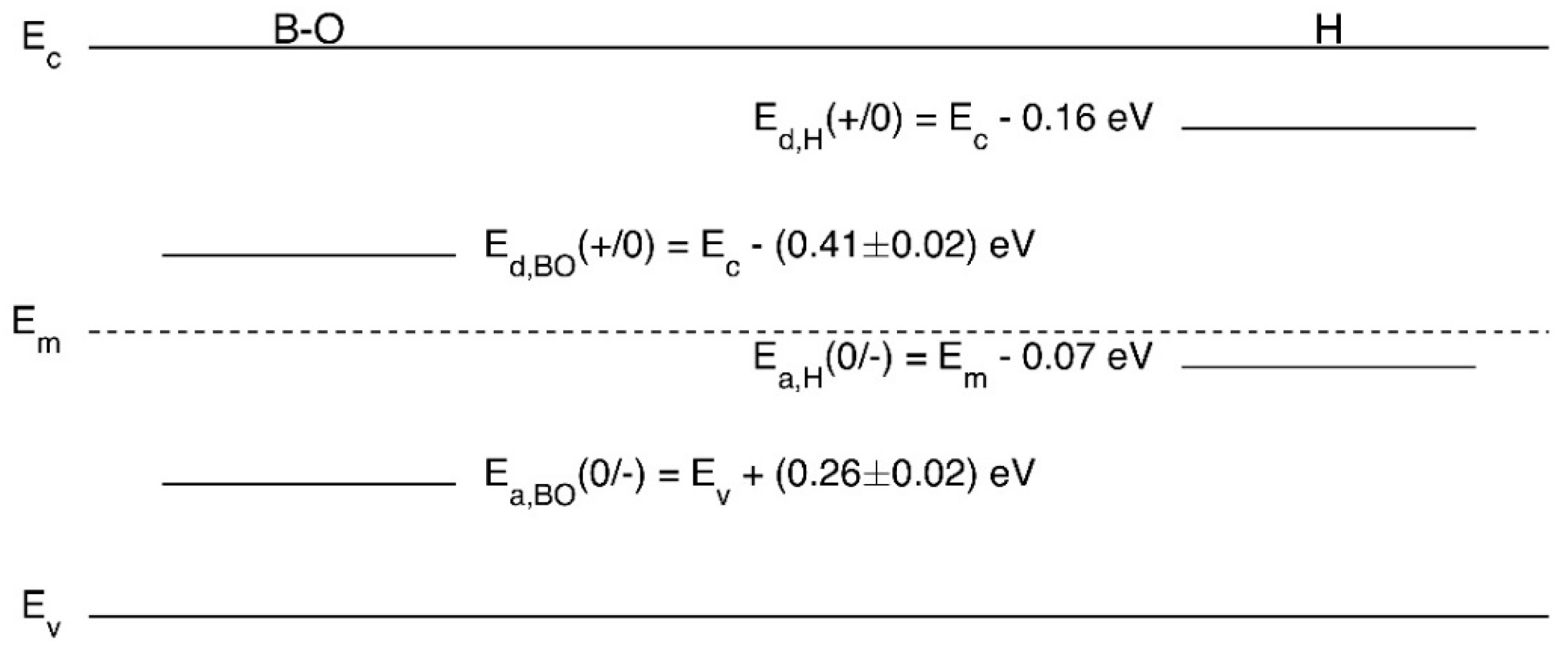
4.1. Role of Hydrogen

Hydrogen is well-known to passivate some metallic and non-metallic defects in silicon [99,100]. Münzer first identified the critical role of hydrogen in the permanent deactivation of B-O defects in 2009 [101]. In particular, solar cells with an antireflection coating consisting of hydrogen-free low-pressure chemical vapour deposited (LPCVD) silicon nitride (SiNx) saw a degradation of performance with exposure to illumination attributed to B-O defects but no subsequent recovery with prolonged illuminated annealing. In contrast, cells coated with hydrogen-containing plasma-enhanced chemical vapour deposited (PECVD) silicon nitride (SiNx:H) displayed a subsequent recovery of open circuit voltage and efficiency with illuminated annealing. Subsequent work by various groups has provided strong evidence for the role of hydrogen in the permanent deactivation process. Wilking et al. showed that the degree of bulk hydrogenation in a remote hydrogen plasma (instead of the commonly used PECVD SiNx:H layers as hydrogen source) correlates with the kinetics of passivation [102] as well as the expected release of hydrogen from boron-hydrogen pairs [87]. Wilking et al. [103] and Walter et al. [104] showed that the firing step mainly responsible for contact formation has a significant impact on the kinetics of passivation most probably as it determines the degree of hydrogenation of the silicon bulk. Also, it was observed that increasing the hydrogen content in dielectric layers can lead to an increase in the hydrogen concentration within the silicon, which correlates well with an acceleration of the passivation [102,103,105,106,107,108].

4.2. Manipulation of Hydrogen Charge States

In silicon, interstitial hydrogen is a negative-U impurity that can assume three different charge states, taking on either a positive (H+), neutral (H0) or negative (H) charge state [109]. The charge state has important implications for the diffusivity and reactivity of the hydrogen [110,111]. For example, the diffusion of both H+ and H is impeded by the attraction to ionised dopant atoms. In contrast, H0 can move freely without the influence of electrostatic effects and has a diffusivity orders of magnitude higher than that of H+ and H [110,112,113,114].
The fractional charge state distributions of hydrogen in silicon are determined by the availability of free electrons in the lattice. In thermal equilibrium, this is heavily dependent on the background doping of the silicon. For p-type silicon, due to a deficiency of electrons, almost all hydrogen is H+. For n-type silicon, due to an excess of electrons, almost all hydrogen is H. For both p-type and n-type silicon, H0 is always a minority charge species, present in only minute concentrations.
However, the fractional charge state distributions determined by the dominant conductivity of the silicon material can be overcome through the use of minority carrier injection. Minority carrier injection can be achieved by using illumination and can lead to substantial increases in the concentration of highly mobile and reactive H0 [111,115]. Some studies have discussed the influence of modulating the charge state of B-O defects and hydrogen for the passivation of B-O defects [87,102,116,117,118,119]. One study, in particular, demonstrated a correlation between the theoretically predicted concentrations of H0 and the regeneration reaction rate using a quasi-Fermi based model [119], highlighting the critical role of manipulating hydrogen charge states to increase the concentration of the minority hydrogen charge species to enable B-O defect passivation. Nevertheless, it remains unclear what species of hydrogen and/or B-O defect is required for the passivation reaction to take place. This uncertainty is partly due to the proximity of the reported donor and acceptor levels of the B-O defect [120] with the energy level at which the majority hydrogen charge state switches from H+ to H (see Figure 2) [109].

4.3. Alternative Theory for Permanent Deactivation and Confusion Related to the Involvement of Hydrogen

Despite evidence from numerous authors on the involvement of hydrogen [87,101,107,116], there has been some debate over the role of hydrogen in the regeneration process [80]. In particular, it has been suggested that thermal effects during fast firing and the impact of plasma processing are responsible for the permanent deactivation of the defects, rather than the introduction of hydrogen [72,121]. One theory was proposed, suggesting that the fast cooling rates reduce the concentration of interstitial boron-oxygen pairs (Bi-O2) and increase the sinking efficiency of boron nano-precipitates, which then determines the rate constant for regeneration [80]. However, subsequent studies have confirmed the critical role of the presence of a hydrogen-containing dielectric layer during firing and that the firing process alone cannot lead to complete suppression of B-O defect formation, nor is it purely caused by exposure to plasma processing [87,122,123].
Subsequent attempts have also been made to prepare samples containing no hydrogen, using lean hydrogen dielectrics deposited at temperatures below 200 °C, with no following high-temperature process to introduce hydrogen into the silicon bulk [124]. These samples were observed to undergo permanent deactivation of the B-O defect, albeit at a rate many orders of magnitude slower than that with the intentional introduction of hydrogen. The authors argued that this demonstrated that hydrogen is not required for regeneration to take place but instead passivates other defects leading to higher lifetimes and hence carrier concentrations. It is, however, extremely challenging and perhaps impossible, to prepare samples containing no hydrogen. Hydrogen can be unintentionally introduced into silicon during a variety of processing steps such as ion-beam or chemical processing [125,126]. Even a dilute HF dip at room temperature can result in significant amounts of atomic hydrogen diffusing several microns into the silicon [126]. With appropriate processing conditions and sufficient time, hydrogen can diffuse throughout a silicon wafer even at temperatures below 100 °C [127]. While high temperatures are often thought to be critical for introducing hydrogen to silicon solar cells, this is much more likely a function of the temperature required to release hydrogen from current commercial dielectrics than due to the limited diffusivity of the hydrogen within the silicon. The most logical conclusion to draw from this study [124] is then that samples containing much less hydrogen demonstrated a much slower regeneration rate when compared to samples with higher hydrogen concentrations.

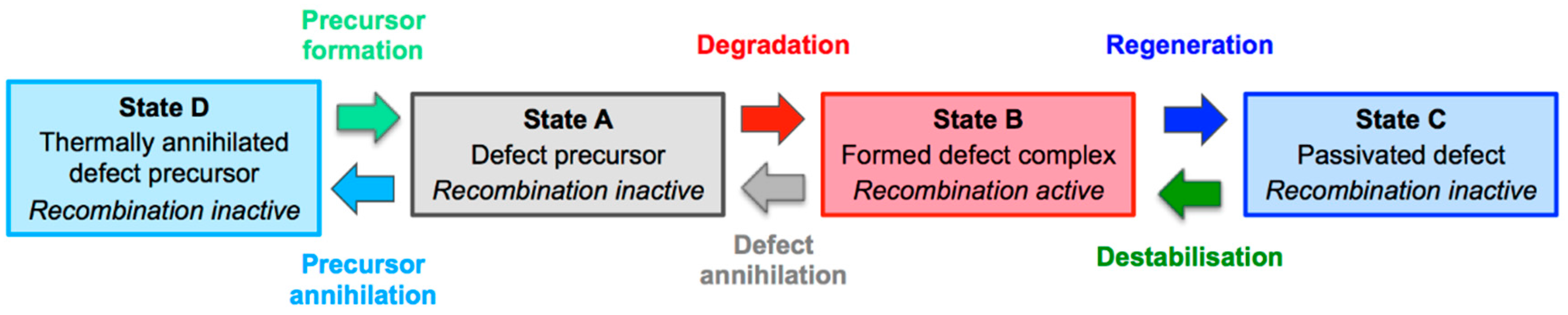
4.4. Role of Defect Formation

In addition to providing a manipulation of hydrogen charge states to enable defect passivation, illumination also plays a critical role in accelerating the formation of defects, simply because a fast passivation process requires defects to form in the first place. On the one hand, a quadratic dependence of the defect formation rate on the equilibrium hole concentration (p0) was observed [24,27,28,94,128]. On the other hand, a dependence of the defect formation rate on the illumination intensity was also observed for low illumination intensities, up to approximately 0.01 suns, at which the reaction rate saturated [8,129]. This illumination intensity corresponds to a saturation of the electron dependence for the reaction with an excess electron concentration on the order of 1 × 1011 cm−3 [130]. Above such excess electron concentrations, the reaction rate in p-type silicon is determined by the background boron-doping concentration, typically on the order of 1 × 1016 cm−3. However, Hamer et al. demonstrated that this fundamental limit of the defect formation rate imposed by the background doping concentration could be overcome by driving the silicon into high-injection conditions using high-intensity laser illumination [131]. It was proposed that the increased reaction rate with high-intensity illumination could be due to a dependence of the reaction rate on the total hole concentration, rather than the equilibrium hole concentration. This hypothesis has subsequently been confirmed by multiple authors [132,133]. This breakthrough enabled full defect formation within four seconds, compared to typical defect formation processes requiring minutes to hours at temperatures below 200 °C using low-intensity illumination (in the order of ~1-sun equivalent illumination) [134].
The defect formation rate has important implications for the ability to eliminate B-O related LID [88,89]. In particular, for conventional low-temperature processes, the defect formation rate is typically slower than that for passivation, hence resulting in a decay and subsequent recovery of lifetime during regeneration processes. Therefore, the ability to passivate B-O defects is limited by the availability of the defects for passivation [89]. Increasing the defect formation rate is therefore critical to accelerating the process of LID mitigation. Increasing the defect formation rate at a given temperature also increases the effectiveness of LID mitigation during illuminated annealing processes (the ratio of passivated to inactive defects). Higher defect formation rates enable the use of higher processing temperatures without sacrificing the effectiveness of LID mitigation [89,93]. The increased temperatures can lead to a further acceleration of the processes due to the exponential dependence of the reaction rates on processing temperature as well as the increase in carrier concentrations and lifetime at higher temperatures [133,135]. However, if an excessively high temperature is used, an incomplete regeneration will result [87]. Subsequently, the temperature is carefully chosen based on the illumination intensity used and typically in the range of 200–300 °C.

4.5. Rapid Laser-Based Processes for LID Elimination

The improved fundamental understanding of defect formation and the mechanisms involved in the permanent deactivation of B-O defects have enabled the development of rapid illuminated processes for eliminating LID. The requirement of high-intensity illumination to accelerate defect formation and for hydrogen charge state manipulations lean towards the use of laser-based hydrogenation processes [136]. Localised laser-based hydrogenation processes were demonstrated by Wilking et al. with time-constants for the regeneration reaction on the order of 0.1 s, provided that defects had been pre-formed [105]. A subsequent study using full-area laser-illumination demonstrated the ability to simultaneously form and passivate B-O defects to completely eliminate B-O related LID within ten seconds on standard aluminium back surface field solar cells, in a time-frame suitable for mass production [137,138]. These rapid processes were performed at a temperature of approximately 300 °C, substantially higher than that used for effectively mitigating B-O related LID in previous studies.

5. Eliminating B-O LID during Cell and Module Fabrication

Although p-type Cz wafers are subject to B-O related LID, a key strength of p-type cell technologies is that they naturally incorporate processes that can enable the elimination of the LID [139]. For industrial p-type solar cells, hydrogen is introduced throughout the silicon bulk during conventional cell processing. This natural introduction of hydrogen allows for a relatively simple modification to the production process to enable the mitigation of B-O related LID during cell or module fabrication. The processing sequence for the fabrication of typical passivated emitter, rear contact (PERC) solar cells is shown in Figure 3. The use of PECVD SiNx:H on the front surface as an antireflection coating creates a source of hydrogen in the device structure that can be manipulated with subsequent processing. In addition, rear surface passivation layers such as PECVD hydrogenated aluminium oxide (AlOx:H) and SiNx:H provide additional hydrogen sources. However, it should be noted that even though the AlOx:H layer may contain hydrogen, it can inhibit the diffusion of hydrogen from the overlying, hydrogen-rich SiNx:H layer into the bulk silicon and retard the regeneration rate [102].
The co-firing process for forming the screen-printed metal contacts is another crucial process for the hydrogenation of B-O defects. This process acts to release hydrogen from the dielectric layers [103] and can enable the diffusion of hydrogen into the silicon and throughout the bulk [140,141,142,143]. The high temperatures used for co-firing, typically in the vicinity of 700–900 °C, overcome issues with trapping, significantly increase the generation of H0 and enhance the diffusivity of hydrogen [111].

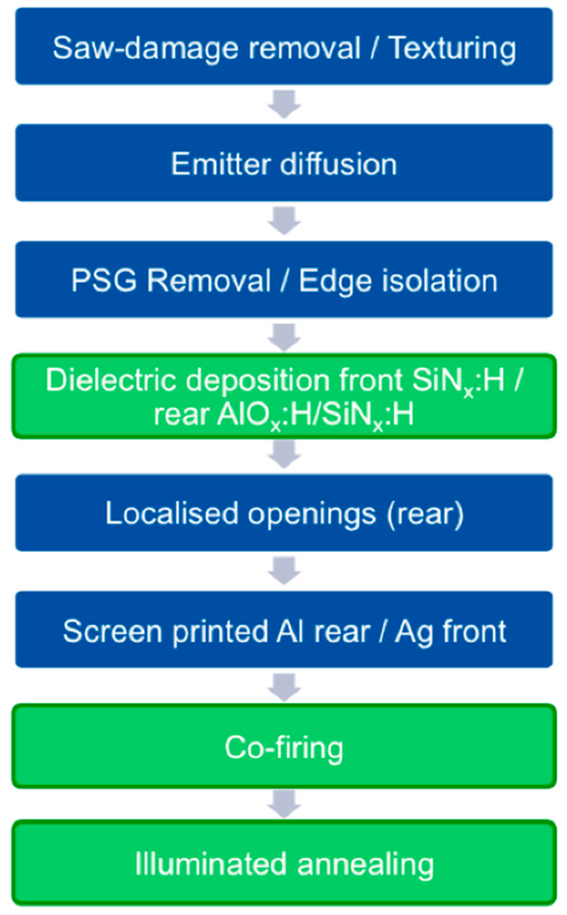
5.1. LID Mitigation during Cell Fabrication

With hydrogen distributed throughout the cell during the co-firing process, a short-illuminated process can be used to form the B-O defects and provide the required hydrogen charge state manipulation to enable the regeneration of the B-O defects. This illuminated process can be achieved during the cool-down section of the high-temperature co-firing process, or as a separate thermal process after co-firing. Several companies, including Centrotherm (Blaubeuren, Germany), Despatch Industries (Mineapolis, MN, USA), Schmid (Freudenstadt, Germany), Asia Neo Tech (Taoyuan City, Taiwan), DR Laser (Wuhan, China) and Folungwin (Dongguan Shi, China) have tools available for LID mitigation that can reduce the extent of LID by approximately 75–80% [144,145,146,147]. For tools with LID mitigation processes integrated into tools for the fast-firing of the metallisation contacts, any potential changes to belt speed resulting from the requirements of future pastes could directly impact B-O LID mitigation. As a result, standalone tools for B-O LID mitigation offer more flexibility with possible future processing changes. They also allow PV module manufacturers to perform LID stabilisation processes on cells fabricated by other manufacturers, before module encapsulation. These LID mitigation tools are tending towards higher and higher illumination intensities to accelerate the process and improve performance.
Currently, most tools are using intensities in the range of 5–20 suns [144,145,146,147]. The illumination intensities used leads to industrial belt-furnace based tools typically requiring processing times of 25–45 s per wafer for the process. The requirement for high-throughput processes with an average of one wafer being processed every second (current industrial standard) thus means that multiple samples must be processed simultaneously. However, laser-based tools are capable of substantially higher illumination intensities, with a correlating decrease in process time. An alternative to the use of high-intensity illumination is the application of current injection to stabilise the cells. In this instance, cells are coin-stacked, with current passing through the entire stack [148]. However, this process results in additional stress and handling of the wafers and potentially an inhomogeneous heating of the wafers, which could reduce the effectiveness of the LID mitigation.
One potential issue with eliminating LID at the cell level, is that during module fabrication the cells are exposed to high temperatures. During soldering localised regions of the cells are exposed to temperatures >230 °C for few seconds and the whole module is exposed to temperatures in the vicinity of 150 °C for up to 15 min during encapsulation. Applying additional thermal processes after an LID mitigation process can destabilise the passivation [83], allowing the material to once again degrade when exposed to illumination. Although a 15-min process at 150 °C is expected to destabilise less than 5% of the passivated defects, due to the large activation energy of the destabilisation reaction, any increase in temperature can lead to a significant increase in the number of defects that are destabilised. For example, increasing the temperature to 200 °C is expected to result in the destabilisation of approximately 20% of the passivated defects.
While destabilisation after regeneration is a potential issue for long-term performance, any condition in the field that results in a heating of the modules that could enable destabilisation, typically occurs in the presence of illumination. Hence, any defects destabilised during module encapsulation will tend to go back towards a passivated state under field operation.

5.2. B-O LID Mitigation during Module Encapsulation

Alternatively, LID mitigation can potentially be performed during encapsulation. Doing so has the advantage that module encapsulation is the last process in the fabrication sequence, therefore avoiding any subsequent destabilisation of the passivated defects during fabrication. LID mitigation can be performed using either current injection or with illumination, noting that in the latter case, significant modifications to existing lamination tools are required to enable illumination, potentially using transparent diaphragms. As a result, it would appear that implementing LID mitigation processes during module encapsulation using current injection is a much simpler approach. Using this method, Lee et al. demonstrated an 80% reduction in the extent of LID compared to a 60% reduction for regeneration processes performed at the cell level [15]. Although no processing details were given, the current requirements during lamination are on the order of 1 sun equivalent to have complete regeneration of the defects.

5.3. Natural Recovery from B-O Related LID during Operation in the Field

With an internal hydrogen source distributed throughout the bulk of the silicon from cell fabrication, normal operating conditions in the field can enable a natural recovery from B-O related defects [15,16,92]. During operation, modules can easily reach temperatures in excess of 50 °C, which is sufficient to enable a recovery of module performance. Lee et al. reported that within 700 h of operation at 50 °C with maximum power-point operation, the open circuit voltage (VOC) loss due to LID had been reduced by 40%. An acceleration of this recovery can be achieved by leaving modules in open circuit, which is typical for modules during initial stages of installation. In open circuit condition at 60 °C, full recovery can be observed within 200 h of continuous illumination [15,48,149]. However, the time for a module to recover is heavily dependent on the mounting construction, geographical location of mounting and the time of year when the modules are installed, all of which can heavily influence the operating temperatures of the module [16]. These dependencies can result in recovery times ranging from several days to several years. The uncertainty of module outputs by relying on a natural recovery of the modules in the field could potentially create issues with financing projects. It is much more desirable that the long-term efficiency is known, which lends towards the implementation of LID mitigation processes during industrial solar cell or module fabrication.

6. Summary

B-O related LID has been an issue for photovoltaic industry since its early years and even now there is still a debate in relation to the fundamental properties of the defect. As a result, different strategies of avoidance were developed in the past, however, as all of these strategies where a trade-off between remaining B-O related LID losses and economic and technological drawbacks, BO-LID remained a serious problem. Over the last decade, a new approach was developed which focuses not on the avoidance of B-O defects but rather their neutralisation using illuminated annealing, or more specifically with carrier injection. Within this new approach, it is generally believed that hydrogen plays a key role in passivating the defects, hence the importance of using a hydrogen-containing dielectric layer with a subsequent high-temperature firing process to inject hydrogen throughout the bulk. This process improves the bulk lifetime of the material and can thermally annihilate B-O defect precursors, leading to a reduced extent of degradation and an increased minority carrier lifetime. During illuminated annealing, high intensity illumination can be used to accelerate defect formation and the charge state control of hydrogen and B-O defects is used to induce a long-lasting passivation of B-O defects. These developments have resulted in a number of industrial solutions for mitigating B-O related LID. In consequence, it seems now possible to eliminate B-O related LID completely within the manufacturing process without any drawbacks related to using alternative silicon materials and finally close the B-O related LID topic, at least for industrial applications.

Acknowledgments

Part of this work was funded by the German Federal Ministry of Economic Affairs and Energy under contract no. 0325581, 0325450A and 0324001. The content is the responsibility of the authors. Part of this work is funded by the Australian Government through the Australian Renewable Energy Agency (ARENA 1060) and the Australian Centre for Advanced Photovoltaics (ARENA 1-SRI001) and the Australian Research Council (ARC) through DE170100620. The views expressed herein are not necessarily the views of the Australian Government and the Australian Government does not accept responsibility for any information or advice contained herein. Phillip Hamer would like to acknowledge funding from the EPSRC through the Supersilicon Grant (EP/M024911/1).

Author Contributions

Phillip Hamer contributed information on the role of defect formation. Nitin Nampalli and Malcolm Abbott contributed information on the thermal elimination of B-O defects. Svenja Wilking contributed information on the role of hydrogen. Stuart Wenham and Giso Hahn contributed information on the elimination of B-O LID during cell/module fabrication. Brett Hallam and Axel Herguth contributed information on alternative silicon materials for avoiding B-O LID, illuminated annealing and jointly wrote the paper.

Conflicts of Interest

The authors declare no conflict of interest.

References

  1. Edenhofer, O.; Pichs-Madruga, R.; Sokona, Y.; Minx, J.C.; Farahani, E.; Susanne, K.; Seyboth, K.; Adler, A.; Baum, I.; Brunner, S.; et al. Climate Change 2014: Mitigation of Climate Change; IPCC: Geneva, Switzerland, 2014; ISBN 9781107654815. [Google Scholar]
  2. Kuhlbrodt, T.; Rahmstorf, S.; Zickfeld, K.; Vikebø, F.B.; Sundby, S.; Hofmann, M.; Link, P.M.; Bondeau, A.; Cramer, W.; Jaeger, C. An integrated assessment of changes in the thermohaline circulation. Clim. Chang. 2009, 96, 489–537. [Google Scholar] [CrossRef] [Green Version]
  3. Hoffmann, W. PV solar electricity industry: Market growth and perspective. Sol. Energy Mater. Sol. Cells 2006, 90, 3285–3311. [Google Scholar] [CrossRef]
  4. Zheng, C.; Kammen, D.M. An innovation-focused roadmap for a sustainable global photovoltaic industry. Energy Policy 2014, 67, 159–169. [Google Scholar] [CrossRef]
  5. International Technology Roadmap for Photovoltaic: 2016 Results, 8th ed.; VDMA: Berlin, Germany, 2017.
  6. Fischer, H.; Pschunder, W. Investigation of photon and thermal induced changes in silicon solar cells. In Proceedings of the 10th IEEE Photovoltaic Specialists Conference, Palo Alto, CA, USA, 13–15 November 1973; pp. 404–411. [Google Scholar]
  7. Ramspeck, K.; Zimmermann, S.; Nagel, H.; Metz, A.; Gassenbauer, Y.; Birkmann, B.; Seidl, A. Light induced degradation of rear passivated mc-Si solar cells. In Proceedings of the 27th European Photovoltaic Solar Energy Conference, Frankfurt, Germany, 24–28 September 2012; pp. 861–865. [Google Scholar] [CrossRef]
  8. Schmidt, J.; Bothe, K. Structure and transformation of the metastable boron- and oxygen-related defect center in crystalline silicon. Phys. Rev. B 2004, 69, 24107. [Google Scholar] [CrossRef]
  9. Hallam, B.; Abbott, M.; Nærland, T.; Wenham, S. Fast and slow lifetime degradation in boron-doped Czochralski silicon described by a single defect. Phys. Status Solidi Rapid Res. Lett. 2016, 10, 520–524. [Google Scholar] [CrossRef]
  10. Hallam, B.; Kim, M.; Abbott, M.; Nampalli, N.; Nærland, T.; Stefani, B.; Wenham, S. Recent insights into boron-oxygen related degradation: Evidence of a single defect. Sol. Energy Mater. Sol. Cells 2017, 173, 25–32. [Google Scholar] [CrossRef]
  11. Voronkov, V.; Falster, R. The nature of boron-oxygen lifetime-degrading centres in silicon. Phys. Status Solidi B 2016, 13, 712–717. [Google Scholar] [CrossRef]
  12. Niewelt, T.; Sch, J.; Warta, W.; Glunz, S.W.; Schubert, M.C. Degradation of crystalline silicon due to boron–oxygen defects. IEEE J. Photovolt. 2017, 7, 383–398. [Google Scholar] [CrossRef]
  13. Knobloch, J.; Glunz, S.W.W.; Biro, D.; Warta, W.; Schaffer, E.; Wettling, W. Solar cells with efficiencies above 21% processed from Czochroalski grown silicon. In Proceedings of the 25th IEEE Photovoltaic Specialists Conference, Washington, DC, USA, 13–17 May 1996; pp. 405–408. [Google Scholar]
  14. Cho, E.; Lai, J.-H.; Ok, Y.; Upadhyaya, A.D.; Rohatgi, A.; Binns, M.J.; Appel, J.; Guo, J.; Fang, H.; Good, E.A. Light-induced degradation free and high efficiency p-type indium-doped PERC solar cells on Czochralski silicon. In Proceedings of the IEEE 42nd Photovoltaic Specialist Conference (PVSC), New Orleans, LA, USA, 14–19 June 2015; pp. 1–4. [Google Scholar]
  15. Lee, K.; Kim, M.-S.; Lim, J.-K.; Ahn, J.-H.; Hwang, M.-I.; Cho, E.-C. Natural recovery from LID: Regeneration under field conditions? In Proceedings of the 31st European Photovoltaic Solar Energy Conference and Exhibition- EU PVSEC, Hamburg, Germany, 14–18 September 2015; p. 1837. [Google Scholar]
  16. Hallam, B.; Bilbao, J.; Payne, D.; Chan, C.; Kim, M.; Chen, D.; Gorman, N.; Abbott, M.; Wenham, S. Modelling the long-term behaviour of boron-oxygen defect passivation in the field using Typical Meteorological Year Data (TMY2). In Proceedings of the 32nd European Photovoltaic Solar Energy Conference and Exhibition, München, Germany, 21–24 June 2016; pp. 555–559. [Google Scholar] [CrossRef]
  17. Hill, J. Global Solar Market Demand Expected to Reach 100 Gigawatts in 2017, Says SolarPower Europe. Available online: https://cleantechnica.com/2017/10/27/global-solar-market-demand-expected-reach-100-gw-2017-solarpower-europe/ (accessed on 6 November 2017).
  18. Colville, F. Forecast for PV cell production & capex: 2016–2018. In Proceedings of the Oral Presentation at PVCellTech, Kuala Lumpur, Malaysia, 16 March 2016. [Google Scholar]
  19. PV Insights. Available online: http://pvinsights.com (accessed on 6 November 2017).
  20. Glunz, S.W.; Rein, S.; Warta, W.; Knobloch, J.; Wettling, W. On the degradation of Cz-silicon solar cells. In Proceedings of the 2nd World Conference on Photovoltaic Solar Energy Conversion, Vienna, Austria, 6–10 July 1998; pp. 1343–1346. [Google Scholar]
  21. Glunz, S.W.; Rein, S.; Knobloch, J.; Wettling, W.; Abe, T. Comparison of boron-and gallium-doped p-type Czochralski silicon for photovoltaic application. Prog. Photovolt. Res. Appl. 1999, 7, 463–469. [Google Scholar] [CrossRef]
  22. Rein, S.; Diez, S.; Falster, R.; Glunz, S.W. Quantitative correlation of the metastable defect in Cz-silicon with different impurities. In Proceedings of the 3rd World Conference on Photovoltaic Energy Conversion, Osaka, Japan, 11–18 May 2003; pp. 1048–1052. [Google Scholar]
  23. Bothe, K.; Sinton, R.; Schmidt, J. Fundamental boron-oxygen-related carrier lifetime limit in mono-and multicrystalline silicon. Prog. Photovolt. Res. Appl. 2005, 13, 287–296. [Google Scholar] [CrossRef]
  24. Bothe, K.; Schmidt, J. Electronically activated boron-oxygen-related recombination centers in crystalline silicon. J. Appl. Phys. 2006, 99, 013701. [Google Scholar] [CrossRef]
  25. Schmidt, J.; Aberle, A.G.; Hezel, R. Investigation of carrier lifetime instabilities in Cz-grown silicon. In Proceedings of the 26th IEEE Photovoltaic Specialists Conference, Anaheim, CA, USA, 29 September–3 October 1997; pp. 13–18. [Google Scholar]
  26. Lim, S.Y.; Rougieux, F.E.; Macdonald, D. Boron-oxygen defect imaging in p-type Czochralski silicon. Appl. Phys. Lett. 2013, 103, 092105. [Google Scholar] [CrossRef]
  27. Forster, M.; Fourmond, E.; Rougieux, F.E.; Cuevas, A.; Gotoh, R.; Fujiwara, K.; Uda, S.; Lemiti, M. Boron-oxygen defect in Czochralski-silicon co-doped with gallium and boron. Appl. Phys. Lett. 2012, 100, 042110. [Google Scholar] [CrossRef]
  28. Lim, B.; Rougieux, F.; Macdonald, D.; Bothe, K.; Schmidt, J. Generation and annihilation of boron-oxygen-related recombination centers in compensated p-and n-type silicon. J. Appl. Phys. 2010, 108, 103722. [Google Scholar] [CrossRef]
  29. Macdonald, D.; Rougieux, F.; Cuevas, A.; Lim, B.; Schmidt, J.; Di Sabatino, M.; Geerligs, L.J. Light-induced boron-oxygen defect generation in compensated p-type Czochralski silicon. J. Appl. Phys. 2009, 105, 093704. [Google Scholar] [CrossRef]
  30. Geilker, J.; Kwapil, W.; Rein, S. Light-induced degradation in compensated p- and n-type Czochralski silicon wafers. J. Appl. Phys. 2011, 109. [Google Scholar] [CrossRef]
  31. Sumino, K.; Harada, H.; Yonenaga, I. The origin of the difference in the mechanical strengths of Czochralski-grown silicon and float-zone-grown silicon. Jpn. J. Appl. Phys. 1980, 19, L49. [Google Scholar] [CrossRef]
  32. Grant, N.E.; Rougieux, F.E.; MacDonald, D.; Bullock, J.; Wan, Y. Grown-in defects limiting the bulk lifetime of p-type float-zone silicon wafers. J. Appl. Phys. 2015, 117, 055711. [Google Scholar] [CrossRef]
  33. Rougieux, F.E.; Grant, N.E.; Macdonald, D. Thermal deactivation of lifetime-limiting grown-in point defects in n-type Czochralski silicon wafers. Phys. Status Solidi Rapid Res. Lett. 2013, 7, 616–618. [Google Scholar] [CrossRef]
  34. Niewelt, T.; Selinger, M.; Grant, N.E.; Kwapil, W.; Murphy, J.D.; Schubert, M.C. Light-induced activation and deactivation of bulk defects in boron-doped float-zone silicon. J. Appl. Phys. 2017, 121, 185702. [Google Scholar] [CrossRef]
  35. Hoshi, K.; Isawa, N.; Suzuki, T.; Ohkubo, Y. Czochralski silicon crystals grown in a transverse magnetic field. J. Electrochem. Soc. 1985, 132, 693–700. [Google Scholar] [CrossRef]
  36. Organ, A.E.; Riley, N. Oxygen transport in magnetic Czochralski growth of silicon. J. Cryst. Growth 1987, 82, 465–476. [Google Scholar] [CrossRef]
  37. Zulehner, W. Czochralski growth of silicon. J. Cryst. Growth 1983, 65, 189–213. [Google Scholar] [CrossRef]
  38. Nakajima, K.; Murai, R.; Morishita, K.; Kutsukake, K.; Usami, N. Growth of multicrystalline Si ingots for solar cells using noncontact crucible method without touching the crucible wall. In Proceedings of the 38th IEEE Photovoltaic Specialists Conference (PVSC), Austin, TX, USA, 3–8 June 2012; pp. 1830–1832. [Google Scholar] [CrossRef]
  39. Togawa, S.; Izunome, K.; Kawanishi, S.; Chung, S.I.; Terashima, K.; Kimura, S. Oxygen transport from a silica crucible in Czochralski silicon growth. J. Cryst. Growth 1996, 165, 362–371. [Google Scholar] [CrossRef]
  40. Arafune, K.; Sasaki, T.; Wakabayashi, F.; Terada, Y.; Ohshita, Y.; Yamaguchi, M. Study on defects and impurities in cast-grown polycrystalline silicon substrates for solar cells. Phys. B Condens. Matter 2006, 376–377, 236–239. [Google Scholar] [CrossRef]
  41. Möller, H.J.; Funke, C.; Rinio, M.; Scholz, S. Multicrystalline silicon for solar cells. Thin Solid Films 2005, 487, 179–187. [Google Scholar] [CrossRef]
  42. Buonassisi, T.; Istratov, A.A.; Pickett, M.D.; Rakotoniaina, J.-P.; Breitenstein, O.; Marcus, M.A.; Heald, S.M.; Weber, E.R. Transition metals in photovoltaic-grade ingot-cast multicrystalline silicon: Assessing the role of impurities in silicon nitride crucible lining material. J. Cryst. Growth 2006, 287, 402–407. [Google Scholar] [CrossRef]
  43. Stoddard, N.; Wu, B.; Witting, I.; Wagener, M.C.; Park, Y.; Rozgonyi, G.A.; Clark, R. Casting single crystal silicon: Novel defect profiles from BP Solar’s mono2 TM wafers. Solid State Phenom. 2008, 131, 1–8. [Google Scholar] [CrossRef]
  44. Guerrero, I.; Parra, V.; Carballo, T.; Black, A.; Miranda, M.; Cancillo, D.; Moralejo, B.; Jiménez, J.; Lelièvre, J.-F.; Cañizo, C. About the origin of low wafer performance and crystal defect generation on seed-cast growth of industrial mono-like silicon ingots. Prog. Photovolt. Res. Appl. 2014, 22, 923–932. [Google Scholar] [CrossRef] [Green Version]
  45. ITRPV Working Group and Others. International Technology Roadmap for Photovoltaics (ITRPV.net): Results 2015, 7th ed.; ITRPV: Frankfurt, Germany, 2016. [Google Scholar]
  46. Lan, C.W.; Yang, C.F.; Lan, A.; Yang, M.; Yu, A.; Hsu, H.P.; Hsu, B.; Hsu, C. Engineering silicon crystals for photovoltaics. CrystEngComm 2016, 18, 1474–1485. [Google Scholar] [CrossRef]
  47. Kersten, F.; Engelhart, P.; Ploigt, H.-C.; Stekolnikov, A.; Lindner, T.; Stenzel, F.; Bartzsch, M.; Szpeth, A.; Petter, K.; Heitmann, J.; et al. A new mc-Si degradation effect called LeTID. In Proceedings of the 42nd IEEE Photovoltaic Specialists Conference, New Orleans, LA, USA, 14–19 June 2015; pp. 1–5. [Google Scholar]
  48. Fertig, F.; Krauss, K.; Rein, S. Light-induced degradation of PECVD aluminium oxide passivated silicon solar cells. Phys. Status Solidi Rapid Res. Lett. 2015, 9, 41–46. [Google Scholar] [CrossRef]
  49. Nakayashiki, K.; Hofstetter, J.; Morishige, A.E.; Li, T.-T.A.; Needleman, D.B.; Jensen, M.A.; Buonassisi, T. Engineering solutions and root-cause analysis for light-induced degradation in p-type multicrystalline silicon PERC modules. IEEE J. Photovolt. 2016, 6, 860–868. [Google Scholar] [CrossRef]
  50. Zuschlag, A.; Skorka, D.; Hahn, G. Degradation and regeneration in mc-Si after different gettering steps. Prog. Photovolt. Res. Appl. 2016. [Google Scholar] [CrossRef]
  51. Shockley, W.; Read, W.T., Jr. Statistics of the recombinations of holes and electrons. Phys. Rev. 1952, 87, 835. [Google Scholar] [CrossRef]
  52. Hall, R.N. Electron-hole recombination in germanium. Phys. Rev. 1952, 87, 387. [Google Scholar] [CrossRef]
  53. Graff, K.; Pieper, H. The properties of iron in silicon. J. Electrochem. Soc. 1981, 128, 669–674. [Google Scholar] [CrossRef]
  54. Macdonald, D.; Roth, T.; Deenapanray, P.N.K.K.; Bothe, K.; Pohl, P.; Schmidt, J. Formation rates of iron-acceptor pairs in crystalline silicon. J. Appl. Phys. 2005, 98, 083509. [Google Scholar] [CrossRef]
  55. Garandet, J.P. New determinations of diffusion coefficients for various dopants in liquid silicon. Int. J. Thermophys. 2007, 28, 1285–1303. [Google Scholar] [CrossRef]
  56. Trumbore, F.A. Solid solubilities of impurity elements in germanium and silicon. Bell Labs Tech. J. 1960, 39, 205–233. [Google Scholar] [CrossRef]
  57. Rosenits, P.; Roth, T.; Glunz, S.W.; Beljakowa, S. Determining the defect parameters of the deep aluminum-related defect center in silicon. Appl. Phys. Lett. 2007, 91. [Google Scholar] [CrossRef]
  58. Möller, C.; Lauer, K. Light-induced degradation in indium-doped silicon. Phys. Status Solidi Rapid Res. Lett. 2013, 7, 461–464. [Google Scholar] [CrossRef]
  59. Richter, A.; Glunz, S.W.; Werner, F.; Schmidt, J.; Cuevas, A. Improved quantitative description of Auger recombination in crystalline silicon. Phys. Rev. B 2012, 86, 165202. [Google Scholar] [CrossRef]
  60. Schmidt, J.; Lim, B.; Walter, D.; Bothe, K.; Gatz, S.; Dullweber, T.; Altermatt, P.P. Impurity-related limitations of next-generation industrial silicon solar Cells. IEEE J. Photovolt. 2013, 3, 114–118. [Google Scholar] [CrossRef]
  61. Falster, R.J.; Gambaro, D.; Cornara, M.; Olmo, M.; Pagani, M. Effect of high temperature pre-anneal on oxygen precipitates nucleation kinetics in Si. Solid State Phenom. 1997, 57, 123–128. [Google Scholar] [CrossRef]
  62. Haunschild, J.; Reis, I.E.; Geilker, J.; Rein, S. Detecting efficiency-limiting defects in Czochralski-grown silicon wafers in solar cell production using photoluminescence imaging. Phys. Status Solidi Rapid Res. Lett. 2011, 5, 199–201. [Google Scholar] [CrossRef]
  63. Cousins, P.J.; Smith, D.D.; Luan, H.-C.; Manning, J.; Dennis, T.D.; Waldhauer, A.; Wilson, K.E.; Harley, G.; Mulligan, W.P. Generation 3: Improved performance at lower cost. In Proceedings of the 35th IEEE Photovoltaic Specialists Conference (PVSC), Honolulu, HI, USA, 20–25 June 2010; pp. 275–278. [Google Scholar]
  64. Letty, E.; Veirman, J.; Favre, W.; Lemiti, M. Solar energy materials & solar cells bulk defect formation under light soaking in seed-end n-type Czochralski silicon wafers—Effect on silicon heterojunction solar cells. Sol. Energy Mater. Sol. Cells 2017, 166, 147–156. [Google Scholar] [CrossRef]
  65. Yu, X.; Wang, P.; Chen, P.; Li, X.; Yang, D. Suppression of boron—Oxygen defects in p-type Czochralski silicon. Appl. Phys. Lett. 2010, 97, 051903. [Google Scholar] [CrossRef]
  66. Taishi, T.; Huang, X.; Yonenaga, I.; Hoshikawa, K. Dislocation behavior in heavily germanium-doped silicon crystal. Mater. Sci. Semicond. Process. 2002, 5, 409–412. [Google Scholar] [CrossRef]
  67. Newman, R.C. Defects in silicon. Rep. Prog. Phys. 1982, 45, 1163–1210. [Google Scholar] [CrossRef]
  68. Vaqueiro-Contreras, M.; Markevich, V.P.; Halsall, M.P.; Peaker, A.R.; Santos, P.; Coutinho, J.; Öberg, S.; Murin, L.I.; Falster, R.; Binns, J.; et al. Powerful recombination centers resulting from reactions of hydrogen with carbon-oxygen defects in n-type Czochralski-grown silicon. Phys. Status Solidi Rapid Res. Lett. 2017, 8, 6–11. [Google Scholar] [CrossRef]
  69. Wang, Z.; Han, P.; Lu, H.; Qian, H.; Chen, L.; Meng, Q.; Tang, N.; Gao, F.; Jia, Y.; Wu, J.; et al. Advanced PERC and PERL production cells with 20.3% record efficiency for standard commercial p-type silicon wafers. Prog. Photovolt. Res. Appl. 2012, 20, 260–268. [Google Scholar] [CrossRef]
  70. Weaver, J.F. EGEG: LONGi at 22.7% Efficiency—Year End Launch, 40% of Electricity in US from Glass, More. Available online: https://electrek.co/2017/10/24/egeg-longi-at-22-7-efficiency-year-end-launch-40-of-electricity-in-us-from-glass-more/ (accessed on 6 November 2017).
  71. Hallam, B.; Hamer, P.; Kim, M.; Nampalli, N.; Gorman, N.; Chen, D.; Chan, C.; Abbott, M.; Wenham, S. Direct Transitions Between States A and C in the Boron-Oxygen Defect System? Fact or Fiction? In Proceedings of the 43rd IEEE Photovoltaic Specialists Conference, Portland, OR, USA, 5–10 June 2016; pp. 2430–2433. [Google Scholar] [CrossRef]
  72. Walter, D.C.; Falster, R.; Voronkov, V.V.; Schmidt, J. On the equilibrium concentration of boron-oxygen defects in crystalline silicon. Sol. Energy Mater. Sol. Cells 2017, 173, 33–36. [Google Scholar]
  73. Nampalli, N.; Li, H.; Kim, M.; Stefani, B.; Wenham, S.; Hallam, B.; Abbott, M. Multiple pathways for permanent deactivation of boron-oxygen defects in p-type silicon. Sol. Energy Mater. Sol. Cells 2017, 173, 12–17. [Google Scholar] [CrossRef]
  74. Glunz, S.W.; Rein, S.; Warta, W.; Knobloch, J.; Wettling, W. Degradation of carrier lifetime in Cz silicon solar cells. Sol. Energy Mater. Sol. Cells 2001, 65, 219–229. [Google Scholar] [CrossRef]
  75. Glunz, S.W.; Rein, S.; Lee, J.Y.; Warta, W. Minority carrier lifetime degradation in boron-doped Czochralski silicon. J. Appl. Phys. 2001, 90, 2397–2404. [Google Scholar] [CrossRef]
  76. Nagel, H.; Merkle, A.; Metz, A.; Hezel, R. Permanent reduction of excess-carrier-induced recombination centers in solar grade Czochralski silicon by a short yet effective anneal. In Proceedings of the 16th European Photovoltaic Solar Energy Conference, Glasgow, UK, 1–5 May 2000; pp. 1197–1200. [Google Scholar]
  77. Saitoh, T.; Wang, X.; Hashigami, H.; Abe, T.; Igarashi, T.; Glunz, S.; Rein, S.; Wettling, W.; Yamasaki, I.; Sawai, H.; et al. Suppression of light degradation of carrier lifetimes in low-resistivity CZ—Si solar cells. Sol. Energy Mater. Sol. Cells 2001, 65, 277–285. [Google Scholar] [CrossRef]
  78. Bothe, K.; Schmidt, J.; Hezel, R. Effective reduction of the metastable defect concentration in boron-doped Czochralski silicon for solar cells. In Proceedings of the 29th IEEE Photovoltaic Specialists Conference, New Orleans, LA, USA, 19–24 May 2002; pp. 194–197. [Google Scholar]
  79. Rougieux, F.E.; Lim, B.; Schmidt, J.; Forster, M.; Macdonald, D.; Cuevas, A. Influence of net doping, excess carrier density and annealing on the boron oxygen related defect density in compensated n-type silicon. J. Appl. Phys. 2011, 110, 063708. [Google Scholar] [CrossRef]
  80. Walter, D.C.; Lim, B.; Bothe, K.; Voronkov, V.V.; Falster, R.; Schmidt, J. Effect of rapid thermal annealing on recombination centres in boron-doped Czochralski-grown silicon. Appl. Phys. Lett. 2014, 104, 042111. [Google Scholar] [CrossRef]
  81. Unsur, V.; Hussain, B.; Ebong, A. Complete recovery of light induced degradation of Cz silicon solar cells with rapid thermal processing. In Proceedings of the 43rd Photovoltaic Specialists Conference, Portland, OR, USA, 5–10 June 2016; pp. 717–719. [Google Scholar] [CrossRef]
  82. Kouhlane, Y.; Bouhafs, D.; Khelifati, N.; Belhousse, S.; Menari, H.; Guenda, A.; Khelfane, A. Effect of rapid thermal processing on light-induced degradation of carrier lifetime in Czochralski p-type silicon bare wafers. J. Electron. Mater. 2016, 45, 5621–5625. [Google Scholar] [CrossRef]
  83. Herguth, A.; Schubert, G.; Käs, M.; Hahn, G. A new approach to prevent the negative impact of the metastable defect in boron doped Cz silicon solar cells. In Proceedings of the 4th IEEE World Conference on Photovoltaic Energy Conversion, Waikoloa, HI, USA, 7–12 May 2006; pp. 940–943. [Google Scholar]
  84. Herguth, A.; Schubert, G.; Kaes, M.; Hahn, G. Avoiding boron-oxygen related degradation in highly boron doped Cz silicon. In Proceedings of the 21st European Photovoltaic Solar Energy Conference, Dresden, Germany, 4–8 September 2006; pp. 530–537. [Google Scholar]
  85. Herguth, A.; Hahn, G. Boron-oxygen related defects in Cz-silicon solar cells degradation, regeneration and beyond. In Proceedings of the 24th European Photovoltaic Solar Energy Conference, Hamburg, Germany, 21–25 September 2009; pp. 974–976. [Google Scholar]
  86. Herguth, A.; Hahn, G. Kinetics of the boron-oxygen related defect in theory and experiment. J. Appl. Phys. 2010, 108, 114509. [Google Scholar] [CrossRef]
  87. Wilking, S.; Beckh, C.; Ebert, S.; Herguth, A.; Hahn, G. Influence of bound hydrogen states on BO-regeneration kinetics and consequences for high-speed regeneration processes. Sol. Energy Mater. Sol. Cells 2014, 131, 2–8. [Google Scholar] [CrossRef]
  88. Hallam, B.J.; Abbott, M.; Nampalli, N.; Hamer, P.G.; Wenham, S.R. Implications of accelerated recombination-active defect complex formation for mitigating carrier-induced degradation in silicon. IEEE J. Photovolt. 2015, 6, 92–99. [Google Scholar] [CrossRef]
  89. Hallam, B.; Abbott, M.; Nampalli, N.; Hamer, P.; Wenham, S. Influence of the formation- and passivation rate of Boron-Oxygen defects for mitigating carrier-induced degradation in silicon within a Hydrogen-Based Model. J. Appl. Phys. 2016, 119, 065701. [Google Scholar] [CrossRef]
  90. Steckenreiter, V.; Walter, D.C.; Schmidt, J. Kinetics of the permanent deactivation of the boron-oxygen complex in crystalline silicon as a function of illumination intensity. AIP Adv. 2017, 7, 035305. [Google Scholar] [CrossRef]
  91. Steckenreiter, V.; Walter, D.; Schmidt, J. Two-stage permanent deactivation of the boron-oxygen-related recombination center in crystalline silicon. Energy Procedia 2017, 124, 799–805. [Google Scholar] [CrossRef]
  92. Hallam, B.; Abbott, M.; Bilbao, J.; Hamer, P.; Gorman, N.; Kim, M.; Chen, D.; Hammerton, K.; Payne, D.; Chan, C.; et al. Modelling kinetics of the boron-oxygen defect system. Energy Procedia 2016, 92, 42–51. [Google Scholar] [CrossRef]
  93. Wilking, S.; Forster, M.; Herguth, A.; Hahn, G. From simulation to experiment: Understanding BO-regeneration kinetics. Sol. Energy Mater. Sol. Cells 2015, 142, 87–91. [Google Scholar] [CrossRef]
  94. Nærland, T.U.; Haug, H.; Angelskar, H.; Sondena, R.; Marstein, E.S.; Arnberg, L. Studying light-induced degradation by lifetime decay analysis: Excellent fit to solution of simple second-order rate equation. IEEE J. Photovolt. 2013, 3, 1265–1270. [Google Scholar] [CrossRef] [Green Version]
  95. Lim, B.; Hermann, S.; Bothe, K.; Schmidt, J.; Brendel, R. Permanent deactivation of the boron-oxygen recombination center in silicon solar cells. In Proceedings of the 23rd European Photovoltaic Solar Energy Conference, Valencia, Spain, 1–5 September 2008; pp. 1018–1022. [Google Scholar]
  96. Lim, B.; Bothe, K.; Schmidt, J. Deactivation of the boron–oxygen recombination center in silicon by illumination at elevated temperature. Phys. Status Solidi Rapid Res. Lett. 2008, 2, 93–95. [Google Scholar] [CrossRef]
  97. Wilking, S.; Ebert, S.; Beckh, C.; Herguth, A.; Hahn, G. Of Apples and oranges: Why comparing bo regeneration rates requires injection level correction. In Proceedings of the 32nd European Photovoltaic Solar Energy Conference, München, Germany, 21–24 June 2016; pp. 487–494. [Google Scholar]
  98. Herguth, A.; Schubert, G.; Käs, M.; Hahn, G. Investigations on the long time behavior of the metastable boron-oxygen complex in crystalline silicon. Prog. Photovolt. Res. Appl. 2008, 16, 135–140. [Google Scholar] [CrossRef]
  99. Hallam, B. High Efficiency Laser-Doped Silicon Solar Cells with Advanced Hydrogenation. Ph.D. Thesis, University of New South Wales, Sydney, Australia, 2014. [Google Scholar]
  100. Hamer, P. Hydrogen Charge States and Dopant Interactions in Crystalline Silicon Solar Cells. Ph.D. Thesis, University of New South Wales, Sydney, Australia, 2014. [Google Scholar]
  101. Münzer, K. Hydrogenated silicon nitride for regeneration of light induced degradation. In Proceedings of the 24th European Photovoltaic Solar Energy Conference, Hamburg, Germany, 21–25 September 2009; pp. 1558–1561. [Google Scholar]
  102. Wilking, S.; Herguth, A.; Hahn, G. Influence of hydrogen on the regeneration of boron-oxygen related defects in crystalline silicon. J. Appl. Phys. 2013, 113, 194503. [Google Scholar] [CrossRef]
  103. Wilking, S.; Ebert, S.; Herguth, A.; Hahn, G. Influence of hydrogen effusion from hydrogenated silicon nitride layers on the regeneration of boron-oxygen related defects in crystalline silicon. J. Appl. Phys. 2013, 114, 194512. [Google Scholar] [CrossRef]
  104. Walter, D.C.; Lim, B.; Bothe, K.; Falster, R.; Voronkov, V.V.; Schmidt, J. Lifetimes exceeding 1 ms in 1-Ω cm boron-doped Cz-silicon. Sol. Energy Mater. Sol. Cells 2014, 131, 51–57. [Google Scholar] [CrossRef]
  105. Wilking, S.; Engelhardt, J.; Ebert, S.; Beckh, C.; Herguth, A.; Hahn, G. High speed regeneration of BO-defects: Improving long-term solar cell performance within seconds. In Proceedings of the 29th European Photovoltaic Solar Energy Conference and Exhibition, Hamburg, Germany, 4–18 September 2014; pp. 366–372. [Google Scholar]
  106. Krugel, G.; Wolke, W.; Geilker, J.; Rein, S.; Preu, R. Impact of hydrogen concentration on the regeneration of light induced degradation. Energy Procedia 2011, 8, 47–51. [Google Scholar] [CrossRef]
  107. Dubois, S.; Tanay, F.; Veirman, J.; Enjalbert, N.; Stendera, J.; Butté, S.; Pochet, P.; Caliste, D.; Mao, Y.; Timerkaeva, D.; et al. The BOLID project: Suppression of the boron-oxygen related light-induced-degradation. In Proceedings of the 27th European Photovoltaic Solar Energy Conference and Exhibition, Frankfurt, Germany, 24–28 September 2012; pp. 749–754. [Google Scholar]
  108. Wilking, S. Das Wasserstoff-Modell der Bor-Sauerstoff-Regeneration. Ph.D. Thesis, University of Konstanz, Konstanz, Germany, 2017. [Google Scholar]
  109. Herring, C.; Johnson, N.M.; de Walle, C.G. Energy levels of isolated interstitial hydrogen in silicon. Phys. Rev. B 2001, 64, 125209. [Google Scholar] [CrossRef]
  110. Mathiot, D. Modeling of hydrogen diffusion in n-and p-type silicon. Phys. Rev. B 1989, 40, 5867–5870. [Google Scholar] [CrossRef]
  111. Hallam, B.J.; Hamer, P.G.; Wenham, S.R.; Abbott, M.D.; Sugianto, A.; Wenham, A.M.; Chan, C.E.; Xu, G.; Kraiem, J.; Degoulange, J.; et al. Advanced bulk defect passivation for silicon solar cells. IEEE J. Photovolt. 2014, 4, 88–95. [Google Scholar] [CrossRef]
  112. Rizk, R.; de Mierry, P.; Ballutaud, D.; Aucouturier, M.; Mathiot, D. Hydrogen diffusion and passivation processes in p- and n-type crystalline silicon. Phys. Rev. B 1991, 44, 6141–6151. [Google Scholar] [CrossRef]
  113. Bonde Nielsen, K.; Nielsen, B.; Hansen, J.; Andersen, E.; Andersen, J. Bond-centered hydrogen in silicon studied by in situ deep-level transient spectroscopy. Phys. Rev. B 1999, 60, 1716–1728. [Google Scholar] [CrossRef]
  114. Estreicher, S.K.; Docaj, A.; Bebek, M.B.; Backlund, D.J.; Stavola, M. Hydrogen in C-rich Si and the diffusion of vacancy-H complexes. Phys. Status Solidi A 2012, 209, 1872–1879. [Google Scholar] [CrossRef]
  115. Hamer, P.; Hallam, B.; Wenham, S.; Abbott, M. Manipulation of hydrogen charge states for passivation of p-type wafers in photovoltaics. IEEE J. Photovolt. 2014, 4, 1252–1260. [Google Scholar] [CrossRef]
  116. Hallam, B.J.; Wenham, S.R.; Hamer, P.G.; Abbott, M.D.; Sugianto, A.; Chan, C.E.; Wenham, A.M.; Eadie, M.G.; Xu, G. Hydrogen passivation of B-O defects in Czochralski silicon. Energy Procedia 2013, 38, 561–570. [Google Scholar] [CrossRef]
  117. Wilking, S.; Herguth, A.; Hahn, G. Influence of hydrogenated passivation layers on the regeneration of boron-oxygen related defects. Energy Procedia 2013, 38, 642–648. [Google Scholar] [CrossRef]
  118. Sun, C.; Rougieux, F.E.; Macdonald, D. A unified approach to modelling the charge state of monatomic hydrogen and other defects in crystalline silicon. J. Appl. Phys. 2015, 117, 045702. [Google Scholar] [CrossRef]
  119. Gläser, M.; Lausch, D. Towards a quantitative model for BO regeneration by means of charge state control of hydrogen. Energy Procedia 2015, 77, 592–598. [Google Scholar] [CrossRef]
  120. Niewelt, T.; Schön, J.; Broisch, J.; Warta, W.; Schubert, M. Electrical characterization of the slow boron oxygen defect component in Czochralski silicon. Phys. Status Solidi Rapid Res. Lett. 2015, 9, 692–696. [Google Scholar] [CrossRef]
  121. Lim, B.; Bothe, K.; Schmidt, J. Accelerated deactivation of the boron-oxygen-related recombination centre in crystalline silicon. Semicond. Sci. Technol. 2011, 26, 095009. [Google Scholar] [CrossRef]
  122. Nampalli, N.; Hallam, B.; Chan, C.; Abbott, M.; Wenham, S. Evidence for the role of hydrogen in the stabilization of minority carrier lifetime in boron-doped Czochralski silicon. Appl. Phys. Lett. 2015, 106, 173501. [Google Scholar] [CrossRef]
  123. Nampalli, N.; Hallam, B.J.; Chan, C.E.; Abbott, M.D.; Wenham, S.R. Influence of hydrogen on the mechanism of permanent passivation of boron-oxygen defects in p-type Czochralski silicon. IEEE J. Photovolt. 2015, 5, 1580–1585. [Google Scholar] [CrossRef]
  124. Walter, D.C.; Schmidt, J. Impact of hydrogen on the permanent deactivation of the boron-oxygen-related recombination center in crystalline silicon. Sol. Energy Mater. Sol. Cells 2016, 158, 91–97. [Google Scholar] [CrossRef]
  125. Seager, C.H.; Anderson, R.A.; Panitz, J.K.G. The diffusion of hydrogen in silicon and mechanisms for unintentional hydrogenation during ion beam processing. J. Mater. Res. 1987, 2, 96–106. [Google Scholar] [CrossRef]
  126. Sopori, B.; Zhang, Y.; Ravindra, N.M. Silicon device processing in H-ambients: H-diffusion mechanisms and influence on electronic properties. J. Electron. Mater. 2001, 30, 1616–1627. [Google Scholar] [CrossRef]
  127. Van Wieringen, A.; Warmoltz, N. On the permeation of hydrogen and helium in single crystal silicon and germanium at elevated temperatures. Physica 1956, 22, 849–865. [Google Scholar] [CrossRef]
  128. Macdonald, D.; Liu, A.; Cuevas, A.; Lim, B.; Schmidt, J. The impact of dopant compensation on the boron-oxygen defect in p-and n-type crystalline silicon. Phys. Status Solidi A 2011, 208, 559–563. [Google Scholar] [CrossRef]
  129. Hashigami, H.; Itakura, Y.; Saitoh, T. Effect of illumination conditions on Czochralski-grown silicon solar cell degradation. J. Appl. Phys. 2003, 93, 4240–4245. [Google Scholar] [CrossRef]
  130. Nærland, T.U.; Angelskår, H.; Marstein, E.S. Direct monitoring of minority carrier density during light induced degradation in Czochralski silicon by photoluminescence imaging. J. Appl. Phys. 2013, 113, 193707. [Google Scholar] [CrossRef]
  131. Hamer, P.; Hallam, B.; Abbott, M.; Wenham, S. Accelerated formation of the boron-oxygen complex in p-type Czochralski silicon. Phys. Status Solidi Rapid Res. Lett. 2015, 9, 297–300. [Google Scholar] [CrossRef]
  132. Schön, J.; Niewelt, T.; Broisch, J.; Warta, W.; Schubert, M. Characterization and modelling of the boron-oxygen defect activation in compensated n-type silicon. J. Appl. Phys. 2015, 118, 245702. [Google Scholar] [CrossRef]
  133. Hamer, P.; Nampalli, N.; Hameiri, Z.; Kim, M.; Chen, D.; Gorman, N.; Hallam, B.; Abbott, M.; Wenham, S. Boron-Oxygen defect formation rates and activity at elevated temperatures. Energy Procedia 2016, 92, 791–800. [Google Scholar] [CrossRef]
  134. Wilson, M.; Edelman, P.; Savtchouk, A.; D’Amico, J.; Findlay, A.; Lagowski, J. Accelerated light-induced degradation (ALID) for monitoring of defects in PV silicon wafers and solar cells. J. Electron. Mater. 2010, 39, 642–647. [Google Scholar] [CrossRef]
  135. Nampalli, N. Characterisation and Passivation of Boron-Oxygen Defects in P-Type Czochralski Silicon. Ph.D. Thesis, University of New South Wales, Sydney, Australia, 2017. [Google Scholar]
  136. Song, L.; Wenham, A.; Wang, S.; Hamer, P.; Shakil, A.; Hallam, B.; Mai, L.; Abbott, M.; Hawkes, E.; Chong, C.; et al. Laser enhanced hydrogen passivation of silicon wafers. Int. J. Photoenergy 2015, 501, 193892. [Google Scholar] [CrossRef]
  137. Hallam, B.J.; Hamer, P.G.; Wang, S.; Song, L.; Nampalli, N.; Abbott, M.D.; Chan, C.E.; Lu, D.; Wenham, A.M.; Mai, L.; et al. Advanced hydrogenation of dislocation clusters and boron-oxygen defects in silicon solar cells. Energy Procedia 2015, 77, 799–809. [Google Scholar] [CrossRef]
  138. Hamer, P.; Hallam, B.; Abbott, M.; Chan, C.; Nampalli, N.; Wenham, S. Investigations on accelerated processes for the boron-oxygen defect in p-type Czochralski silicon. Sol. Energy Mater. Sol. Cells 2016, 145, 440–446. [Google Scholar] [CrossRef]
  139. Hallam, B.; Chen, D.; Kim, M.; Stefani, B.; Hoex, B.; Abbott, M.; Wenham, S. The role of hydrogenation and gettering in enhancing the efficiency of next generation Si solar cells: An industrial perspective. Phys. Status Solidi A 2017, 1700305. [Google Scholar] [CrossRef]
  140. Sheoran, M.; Upadhyaya, A.; Rohatgi, A. Bulk lifetime and efficiency enhancement due to gettering and hydrogenation of defects during cast multicrystalline silicon solar cell fabrication. Solid. State Electron. 2008, 52, 612–617. [Google Scholar] [CrossRef]
  141. Sheoran, M.; Kim, D.S.; Rohatgi, A.; Dekkers, H.F.W.; Beaucarne, G.; Young, M.; Asher, S. Hydrogen diffusion in silicon from plasma-enhanced chemical vapor deposited silicon nitride film at high temperature. Appl. Phys. Lett. 2008, 92, 172107. [Google Scholar] [CrossRef]
  142. Kleekajai, S.; Jiang, F.; Stavola, M.; Yelundur, V.; Nakayashiki, K.; Rohatgi, A.; Hahn, G.; Seren, S.; Kalejs, J. Concentration and penetration depth of H introduced into crystalline Si by hydrogenation methods used to fabricate solar cells. J. Appl. Phys. 2006, 100, 093517. [Google Scholar] [CrossRef]
  143. Kleekajai, S.; Wen, L.; Peng, C.; Stavola, M.; Yelundur, V.; Nakayashiki, K.; Rohatgi, A.; Kalejs, J. Infrared study of the concentration of H introduced into Si by the postdeposition annealing of a SiNx coating. J. Appl. Phys. 2009, 106, 123510. [Google Scholar] [CrossRef]
  144. Fischbeck, G. Keep a LID on it. PV-Magazine, 16 November 2015; 44–47. [Google Scholar]
  145. Hallam, B.; Chan, C.; Payne, D.N.R.; Lausch, D.; Gläser, M.; Abbott, M.; Wenham, S. Techniques for mitigating light-induced degradation (LID) in commercial silicon solar cells. Photovolt. Int. 2016, 33, 37–46. [Google Scholar]
  146. Pernau, T.; Romer, O.; Scheiffele, W.; Reichart, A.; Jooß, W. Rather high speed regeneration of BO-defects: Regeneration experiments with large cell batches. In Proceedings of the 31st European Photovoltaic Solar Energy Conference, Hamburg, Germany, 14–18 September 2015; pp. 918–920. [Google Scholar]
  147. Hallam, B.J.; Chan, C.E.; Chen, R.; Wang, S.; Ji, J.; Mai, L.; Abbott, M.D.; Payne, D.N.R.; Kim, M.; Chen, D.; et al. Rapid mitigation of carrier-induced degradation in commercial silicon solar cells. Jpn. J. Appl. Phys. 2017, 56, 08MB13. [Google Scholar] [CrossRef]
  148. Herguth, A.; Hahn, G. Towards a high throughput solution for boron-oxygen related regeneration. In Proceedings of the 28th European Photovoltaic Solar Energy Conference, Paris, France, 30 September–4 October 2013; pp. 1507–1511. [Google Scholar] [CrossRef]
  149. Fertig, F.; Broisch, J.; Biro, D.; Rein, S. Stability of the regeneration of the boron-oxygen complex in silicon solar cells during module certification. Sol. Energy Mater. Sol. Cells 2014, 121, 157–162. [Google Scholar] [CrossRef]
Figure 1. Simplified diagrammatic representation of the boron-oxygen (B-O) defect system.
Applsci 08 00010 g001
Figure 2. Energy level diagram for B-O defects and interstitial hydrogen showing the donor (Ed) and acceptor (Ea) levels relative to the conduction band (Ec), valence band or mid-gap (Em).
Applsci 08 00010 g002
Figure 3. The process flow for the fabrication of industrial screen-printed PERC solar cells with a rear surface passivation dielectric stack of plasma-enhanced chemical vapour deposited (PECVD) hydrogenated aluminium oxide (AlOx:H) and silicon nitride (SiNx:H). Processes related to the hydrogenation of B-O defects are shown in green. Other processes are shown in blue.
Applsci 08 00010 g003

