Development of a Magnetostrictive FeNi Coated Surface Acoustic Wave Current Sensor


1
China Electric Power Research Institute of State Grid, Beijing 100192, China
2
State Key Laboratory of Acoustics, Institute of Acoustics, Chinese Academy of Sciences, No. 21, Beisihuan West Road, Beijing 100190, China
3
School of Electronic. Electrical and Communication Engineering, University of Chinese Academy of Sciences, Beijing 100049, China
*
Author to whom correspondence should be addressed.
Appl. Sci. 2017, 7(8), 755; https://doi.org/10.3390/app7080755
Submission received: 7 July 2017
/
Revised: 19 July 2017
/
Accepted: 20 July 2017
/
Published: 25 July 2017
(This article belongs to the Section Acoustics and Vibrations)
Abstract
:Featured Application
The developed magnetostrictive FeNi coated Surface acoustic wave sensor with high sensitivity; fast response; strong anti-interference; good linearity and repeatability; and lower hysteresis error will be a potential candidate for current monitoring application in smart grid line testing; metallurgical and power supplies; rail transit safety warnings and rescue.
Abstract
A magnetostrictive FeNi-coated surface acoustic wave (SAW)-based current sensor was proposed in this work. The weak remanence and hysteresis effect of the FeNi itself contributes to suppress the asymmetry in sensor response at increasing and decreasing current. The sensor response was simulated by solving the coupled electromechanical field equation in layered structure considering the magnetostrictive effect and an approach of effective dielectric constant. The effects from the aspect ratio and thickness of the FeNi film on sensor response were analyzed to determine the optimal design parameters. Differential oscillation structure was used to form the sensor, in which, the FeNi thin film was deposited along the SAW propagation of the sensor chip by using RF magnetron sputtering. The magnetostrictive effect of the FeNi coating induced by the magnetic loading generates the perturbation in SAW velocity, and corresponding oscillation frequency. High sensitivity of 10.7 KHz/A, good linearity and repeatability, lower hysteresis error of 0.97% were obtained from the developed prototype 150 MHz SAW FeNi coated current sensor.
1. Introduction
Surface acoustic wave (SAW)-based devices attracts increasing attention for various physical and chemical sensing because they offer some unique performances such as high sensitivity, excellent reproducibility, small size, simple structure, robustness, being passive (batteryless), and remotely queried (wireless). Many proven SAW-based sensors were developed for sensing gas species, temperature, force, torque, and so on [1,2,3,4,5]. Recently, referring to the magnetostrictive thin film as the sensing material or magnetoresistor as the external loaded sensor, a new concept of SAW-based magnetic/current sensor were proposed, allowing possible features of fast response, high sensitivity, strong anti-interference, and small size. The functional magnetostrictive thin-film materials are favored and very promising for high-precision magnetic/current field measurement owing to their large magnetostrictive coefficient, high energy conversion efficiency, fast response and non-contact driving. Kodota et al. subsequently presented a new prototype of SAW magnetic sensor using interdigital transducers (IDTs) made by magnetostrictive Ni electrodes on a quartz substrate and wireless and passive measurement was offered. Obtained magnetic sensitivity was 730 Hz/mT [6,7]. Elhosni et al. proposed a similar SAW magnetic sensor with a magnetostrictive-piezoelectric layered structure of Ni/ZnO/IDT/LiNbO3, and the corresponding finite element modeling (FEM) simulation was performed to predict the sensor performance [8,9]. Using the Galfenol thin film as the sensitive interface, a SAW magnetic field sensor was developed by Li et al. a maximum change of 0.64% in SAW velocity was obtained with a 500 nm Galfenol thick film, but not including further details about the experimental results [10]. Zhou et al. addresses the experimental and theoretical investigations of SAW magnetic sensor structured by TbCo2/FeCo/Y-cut LiNbO3 [11]. Just recently, a magnetostrictive FeCo-coated SAW magnetic/current sensor using the differential oscillation structure was proposed in our previous work, where high sensitivity of 16.6 KHz/A was obtained [12].
As for the magnetoresistor loaded magnetic sensor, Hauser et al. developed a wirelessly interrogable micro-magnetic field sensor using the giant magneto-impedance (GMI) effect in a 30 μm diameter amorphous FeCoSiBNd wire of zero magnetostriction, and a SAW transponder devices, a relative signal sensitivity of 80 dB/T at low magnetic flux density B less than 30 mT, quick response, and a high temperature stability were obtained [13]. Utilizing a reflective delay line pattern loaded a tri-layer GMI sensor, an autonomous magnetic field sensor was realized by Li et al. and a sensitivity of 0.34 dB/Oe are reported experimentally [14,15]. Also, Reindl et al. reported a dexterous design of the configuration of the SAW magnetic/current sensor loaded with magnetoresistor sensor, where wireless and passive measurement for current was realized [16,17], and the obtained current resolution is approximately 5% of full scale (−800~800 A).
Obviously, the magnetostrictive film coated SAW sensor exhibits simpler design, higher magnetic sensitivity and better temperature compensation in sensor structure over the magnetoresistor loaded sensor, and becomes the future research focus. Some magnetostrictive materials with larger magnetostrictive coefficient as FeCo, TbCo2 were advised as the sensitive coating, which produce higher magnetic sensitivity. However, due to the large magnetic remanence and hysteresis effect of these materials mentioned above, there occurs obvious asymmetry in sensor response at increasing and decreasing current, which degrades significantly the sensor performance.
Among the available magnetostrictive materials, the FeNi features very small variation of coercive field and narrow and steep magnetic hysteresis, and additionally, it has excellent rust resistance and better process ability over the FeCo film, which makes it very promising for magnetic/current sensing, and was employed as the sensitive materials in this contribution.
So, the first aim in this work is to perform the simulation on the sensor response by solving the coupled electromechanical field equation in layered structure considering the magnetostrictive effect and approach of effective constant [12], and then to determine the optimal design parameters for FeNi coating preparation by analyzing the effect on sensor response from the film thickness and aspect ratio.
Then, a FeNi-coated SAW based current sensor was constructed, which was composed of a differential SAW delay line oscillator configuration, and magnetostrictive FeNi thin film deposited along the SAW propagation path of the sensing device. The scheme and working principle of the proposed sensor are depicted in Figure 1. YZ-LiNbO3 was utilized as the piezoelectric substrate, which provides larger electromechanical coupling coefficient (4.1%) to reduce the insertion loss of the SAW chip, and linear temperature coefficient of frequency (TCF) contributing to the temperature compensation by using the differential structure mentioned in Figure 1. Additionally, the single phase unidirectional transducers (SPUDTs) with Al electrodes were used to structure the SAW device to reduce the insertion loss [18,19]. The FeNi thin film was then coated on the top surface of the sensing device by RF magnetron sputtering and overlay technique. Prior to FeNi coating, a 50 nm SiO2 film was deposited on the piezoelectric substrate to provide a well protection on interdigital transducers (IDTs) in procedure of FeNi coating. The FeNi film produces magnetostrictive strain stimulated by the electromagnetic field, where the thickness, density and young’s modulus of the FeNi film are changed accordingly, and then the SAW propagation characteristic are modulated in the form of shift in SAW velocity. The applied electromagnetic field can be evaluated by using the corresponding differential oscillation frequency signal. Utilizing the Helmholtz coil system, the developed SAW sensor was characterized, and in comparison to FeCo coated sensor.
2. Simulation on the Sensor Response
Prior to sensor device development, the sensor response was simulated theoretically to extract the optimal design parameters.
In the simulation, the SAW sensor was simplified as a structure composed of a semi-infinite piezoelectric substrate with IDT pattern, a SiO2 coating, and a magnetostrictive FeNi thin film as shown in Figure 2. Also, the theoretical simulation is referring to the way of an analytical resolution of acoustic motion equations in layered structure considering the magnetostrictive effect described in [12], so the influences of different parameters on sensor performances appear clearly. The corresponding coordinate system is shown in Figure 2. Acoustic wave propagates along the x1 axis on the x1 − x2 plane at x3 = 0. All material parameters of the mediums are transformed into the coordinate system. Each material in the layered structure is defined by its physical parameters: stiffness constants (cIijkl), piezoelectric constant (ekij), permittivity constant (εij), and density (ρI) for LiNbO3, stiffness constants ((cIIijkl)) and density (ρII) for SiO2, Young’s modulus (E) and density (ρIII) for FeNi. h1 and h2 express the thicknesses of SiO2 and FeNi, respectively. The corresponding physical parameters for piezoelectric substrate, SiO2, and FeNi are listed in Table 1 [20]. The SAW velocity relating to the electromagnetic field intensity can be calculated by solving the elastic wave equations of each media utilizing corresponding boundary conditions. The following is the specific theoretical simulation.
It is well known that the constitutive equations in a piezoelectric medium are expressed as in [21].
where i, j = 1, 2, 3, K, L = 1, 2, … 6, , and Φ are the density, displacement and electric potential in YZ-LiNbO3, respectively.
The field space of the frequency domain and the frequency slowness field (s) can be characterized by Fourier transform pairs, hence, a general solution of the coupled wave Equation (1) was assumed in the slowness (s) region as
where, s is the SAW slowness, and defined by the reciprocal of the SAW velocity, α is the acoustic attenuation factor in x3 direction.
Substituting Equation (2) into the coupling wave Equation (1), and the Christoffel equation of the piezoelectric substrate in the slowness field is obtained, which is a quadratic polynomial of α, and expressed by
where, αI is the characteristic root, and AI1, 2, 3, 4 are undetermined constants, i.e., eigenvectors.
The necessary condition for the existence of the non-trivial solution in Christoffel equation is det(Γ) = 0, and an eight degree equation about αI was obtained. Γ is the determinant of the coefficient matrix. To ensure the decrease of the acoustic displacement into the substrate, four roots of αI with imaginary part more than zero were picked, that is, αIn (n = 1, 2, 3, 4). Then, Substituting αIn into the Christoffel equation, a set of eigenvectors corresponding to each αIn are deduced. It is clear that only the linear superposition of the solutions as Equation (2) corresponding to αIn (n = 1, 2, 3, 4) can satisfy the Christoffel equation and the boundary conditions. Thus, the integral solution was formed as the linear superposition of the wavelet solution, that is,
where CIn (n = 1, 2, 3, 4) is the weighted factor which determined by the boundary conditions.
Usually, the SiO2 and FeNi can be considered as isotropic media, and their typical matrix representation of acoustic wave equations are defined by
So, the integral solution in acoustic equation of the isotropic SiO2 film is assumed as
Then, substituting Equation (6) into the wave Equation (5), the corresponding Christoffel equation is obtained by
Similarly, the conditions for existence of non-trivial solution in Christoffel equation is that the determinant of the coefficient matrix (Γ) should be zero, that is, det(Γ) = 0. A six degree equation about αI can be deduced. Since the thickness of the SiO2 film is limited, the six roots of (p = 1, 2, …, 6) all satisfy the Christoffel equation, and the integral form of the displacement in the frequency slowness domain is expressed by
where i = 1, 2, 3. AiII is eigenvectors corresponding to apII, CpII (p = 1, 2, …, 6) are the weighted coefficients, and determined by the boundary conditions.
The solution in FeNi thin film is similar to SiO2. And the corresponding integral solution of the displacement in the frequency slowness domain of the FeCo film can be expressed as
where, the corresponding six eigen values and eigenvectors in FeNi film are expressed as apIII and ApIII (p = 1, 2, 3, 4, 5, 6), and CnIII (n = 1, 2, 3, 4) are the weighted coefficients.
There is no free charge distribution in the region of 0 < x3 < h1, h1 < x3 < h1 + h2, and h1 + h2 < x3, which are marked by II, III and G, respectively. Then the potentials ΦII, ΦIII and ΦG satisfying the Laplace equation are introduced to meet the electrical boundary conditions, and the electric displacement components D3 in the x3 direction are determined in the corresponding regions. ΦII, ΦIII, ΦG, , and in the frequency slowness field are expressed by
where, εII, εIII and ε0 are the dielectric constant of the SiO2 layer, FeNi layer and the air dielectric constant, respectively, ε0 = 8.854 × 10⁻¹² (F/m).
The boundary conditions for each surface of the layered media structure shown in Figure 2 are described as below. Firstly, the stress, displacement, and electric potential are continuous at x3 = 0 and x3 = h1, that is,
The normal component of the stress at x3 = h1 + h2 is considered as zero, and the corresponding displacement and electric potential are continuous as
To sum up, there are 21 undetermined unknowns in the Christoffel equation expressed by , , , , , , and . It means that there are 21 equations to determine the unknowns. To simply the calculation, the approach of effective dielectric constant was used.
Accordingly, the εs(s) value corresponding different slowness s can be deduced, and also the surface effective dielectric constant εs(s) curve can be pictured. Usually, εs(s) is a complex number. The slowness sm corresponding to the maximum value of the real part shows the case of metallization at x3 = 0. While the slowness sf corresponding to the zero-crossing of the real part shows the free surface at x3 = 0. According to the reciprocal relationship, the corresponding SAW velocity in metalized surface vm, and velocity in free surface, vf, at x3 = 0, can be obtained, respectively.
Usually, the magnetostriction of FeNi film will be changed by its aspect ratio [23],
where β and β0 are the perturbed and unperturbed magnetostriction of the FeNi film, respectively, and p = l/w is the aspect ratio, l and w are the length and width of FeNi film, respectively. kp is the correlation coefficient, and is set to 7.13 × 10⁻⁴ [23].
Owing to the magnetostrictive nature, the FeNi film would be magnetized under the electromagnetic field, resulting in the changes in FeNi film thickness h and density ρ, which can be written by
where m is the mass of the FeNi film, a0, b0, h2 are the initial length, width and thickness of unperturbed FeNi, respectively, and obviously m = ρIII × (a0 × b0 × h2).
Moreover, the young’s modulus (E) of the FeNi will also be modulated by the electromagnetic field intensity (H), and can be taken experimentally by using the laser resonance method [24]. Correspondingly, the elastic coefficient of the FeNi will also be expressed as
where the Poissoncoefficient of FeNi, uF, was considered as constants irrelevant to the electromagnetic field, and it was set to 0.3.
Hence, using above equations and the measured relationship between the young’s modulus of FeNi and the magnetic field (Figure 3), the shift in SAW velocity shift depending on the applied electromagnetic field can be calculated. Also, considering the relationship between the electromagnetic field intensity (H) and current (A) described by the Biot-Savart law [25],
where, μ0 denotes the permeability in vacuum. l expresses the distance between the sensor chip and wires, and is set to 1 cm in this calculation, the sensitivity in current sensing can be evaluated theoretically. Furthermore, the influence of FeNi thickness and aspect ratio (a0/b0) on sensor response can be analyzed using the physical parameters listed in Table 1. The sensor response was defined as the difference between the perturbed and unperturbed SAW velocity. The given electromagnetic field intensity and working frequency of sensor in the calculation are set to 200 Oe and 150 MHz. Nonlinear relationship was observed between the sensor response and FeNi thickness, as shown in Figure 4a. The sensor response increases rapidly with increasing the FeNi thickness up to ~0.5 μm and then reaches the max response value. Hence, the optimal value in FeNi thickness is advised to ~500 nm. Additionally, the effect of the aspect ratio of the FeNi on sensor response was also analyzed as shown in Figure 4b. With increasing the aspect ratio (1:1 to 2:1), larger sensor response was observed. However, lager aspect ratio will lengthen SAW propagation path, resulting in increase of the acoustic propagation attenuation. So, in our opinion, proper increase in aspect ratio of FeNi film is an effective way to improve the sensor sensitivity.
Then, referring to the Biot-Savart law mentioned Equation (16) and velocity-frequency relationship of Δv/vs = Δf/f0 (Δv and Δf are the shift in SAW velocity vs and sensor frequency f0), the current sensitivity of the 150 MHz SAW sensor coated with 500 nm FeNi (aspect ratio is set to 2:1) was calculated as shown in Figure 5, and sensitivity of ~11 KHz/A was expected.
3. Technique Realization
3.1. Sensor Chip
Two SAW delay lines with two photolithographically defined 100 nm Al interdigital transducers (IDTs) separated by a 2.5 mm length of propagation path were reproducibly fabricated on a same piezoelectric YZ LiNbO3 wafer. The launch and receive SPUDT pairs were set to 60 and 30, respectively. The acoustic aperture is 100λ (λ stands for the wavelength corresponding operation frequency of 150 MHz: 23.19 μm). Following the preparation of delay line patterns, a SiO2 thin film (50 nm) was deposited on the SAW device surface to protect the electrodes in process of FeNi coating by using the plasma enhanced chemical vapor deposition (PECVD). Prior to FeNi coating, the SiO2 film surface was cleaned of any contaminants by a routine cleaning procedure involving rinsing in acetone solution, a DI water rinse and drying by N2. Then, the magetostrictive FeNi film with various aspect ratio (1:1, 1.5:1 and 2:1) was deposited onto the sensing device surface by RF magnetron sputtering (JGP-560C magnetron sputtering equipment) and overlay technique from a FeNi target (nominal composition). The base pressure is 2 × 10⁻⁴ Pa. The Ar was used as the sputtering gas, and corresponding pressure is set to 1 Pa. The power density of the target was 400 V (DC) × 80 mA/p (35 mm)2. Various FeNi thicknesses (300, 500 and 700 nm) were obtained by controlling the sputtering time. The specific technological process is depicted in Figure 6. Figure 7 is the picture of the developed FeNi-coated sensor chip, and FeNi coating was indicated by the dark area. The surface morphology of FeNi coating was observed by JSM5600-Lv scanning electron microscopy (SEM) (JEOL, Tokyo, Japan), as shown in Figure 8. It can be seen that the prepared FeNi film are densely and uniformly distributed. To make the comparison, 500 nm FeCo film with aspect ratio of 2:1 was also deposited onto the similar SAW device surface to form a FeCo-coated sensor.
Next, the FeNi-coated SAW sensor chips with various FeNi thickness (300, 500 and 700 nm) were characterized by using the network analyzer, as shown in Figure 9. With increases in FeNi thickness, the operation frequency of the sensor chip decreases owing to the mass loading effect from the FeNi coating. The measured operation frequency and insertion loss of the sensor chip with 300, 500 and 700 nm FeNi (with aspect ratio of 2:1) are 149.9 MHz and 5 dB, 149.7 MHz and 7 dB, 149.6 MHz and 8 dB, respectively.
3.2. FeNi Coated Current Sensor
After the preparation of the FeNi coated sensor chip, the launch and receive transducers of the SAW chips were connected to the oscillation loop composed of amplifier, phase shifter, and mixer, and forms the differential oscillator, as shown in Figure 1. To improve the frequency stability of the oscillator, the oscillation was tuned on the frequency corresponding to lowest insertion loss of the SAW device by adjusting the inductor or capacitor values in phase shifter. The produced differential frequency signal was connected at 20 points per second by the frequency acquisition module (FAM) made by field programmable gate arrat (FPGA), gathered and plotted by the personal computer in real time. Due to the magetostrictive effect, the FeNi produces the magnetostrictive strain and ΔE effect, where the thickness, density and young modulus of the FeNi film are changed accordingly, and then the corresponding changes in differential oscillation frequency signal was picked to evaluate the current to be measured.
4. Sensor Experiment and Discussion
4.1. Experimental Setup
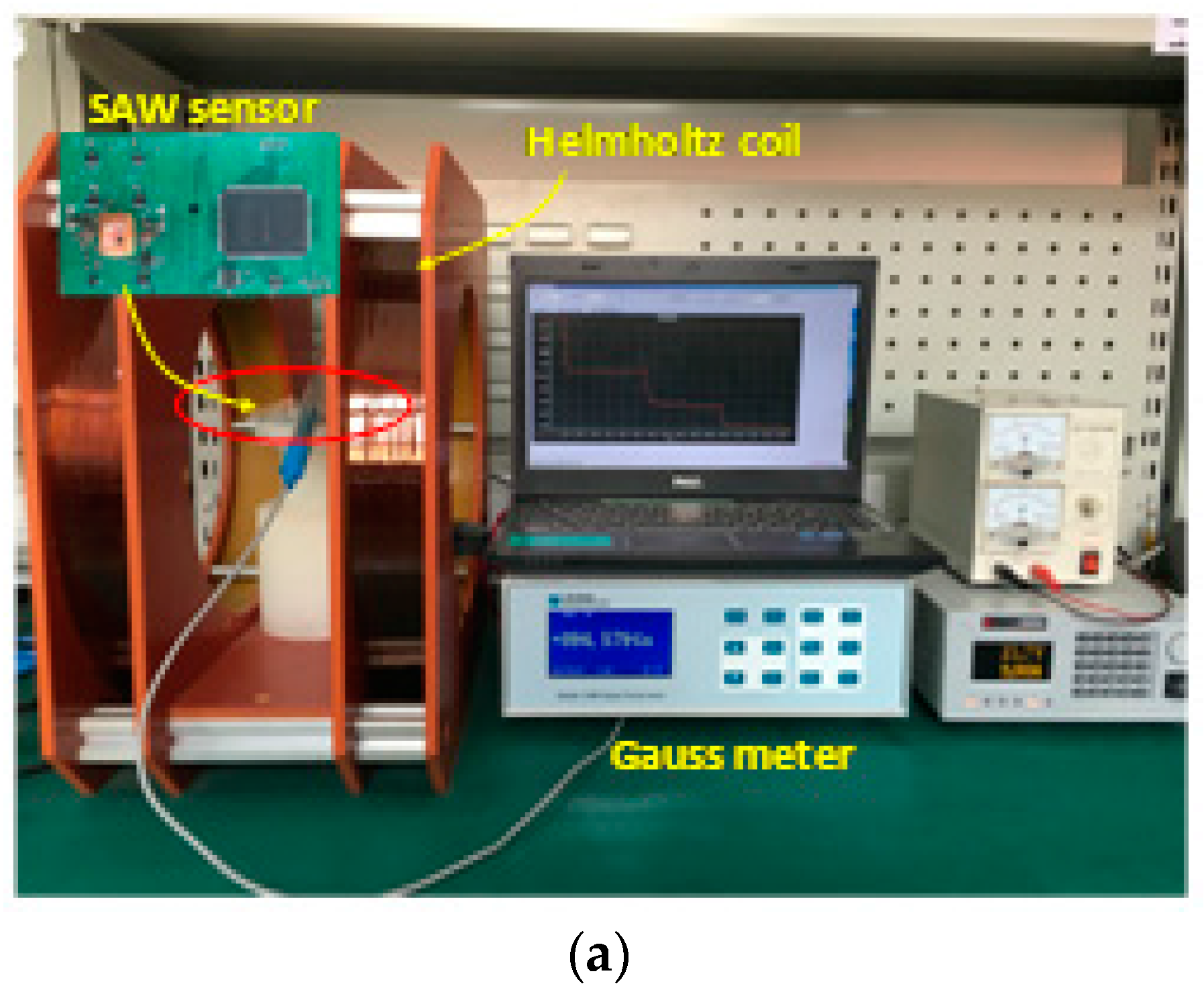
The physical map and schematic diagraph of the experimental setup for current sensor characterization were shown in Figure 10. The experimental setup was composed of the developed SAW current sensor, DC current source (YangZhou Huatai Electronics Co., Ltd., Yangzhou, China), Helmholtz coil (Tianduan Industry Co., Ltd, Shanghai, China) for stimulating the magnetic field under giving current, PC and Gauss meter (Tianduan Industry Co., Ltd) for calibration (Figure 10a). Usually, the strongest magnetic field intensity and the best uniformity occur at the central axis of the Helmholtz coil, hence, the sensor was positioned at the central axis of the platform in the middle of the coil. As shown in Figure 10b, the applied current for Helmholtz coil stimulates electromagnetic field, and the corresponding sensor response induced by the magnetostrictive effect was taken from the oscillation frequency signal connected at 1 point per 50 ms by the FPGA.
4.2. Baseline Noise Measurement
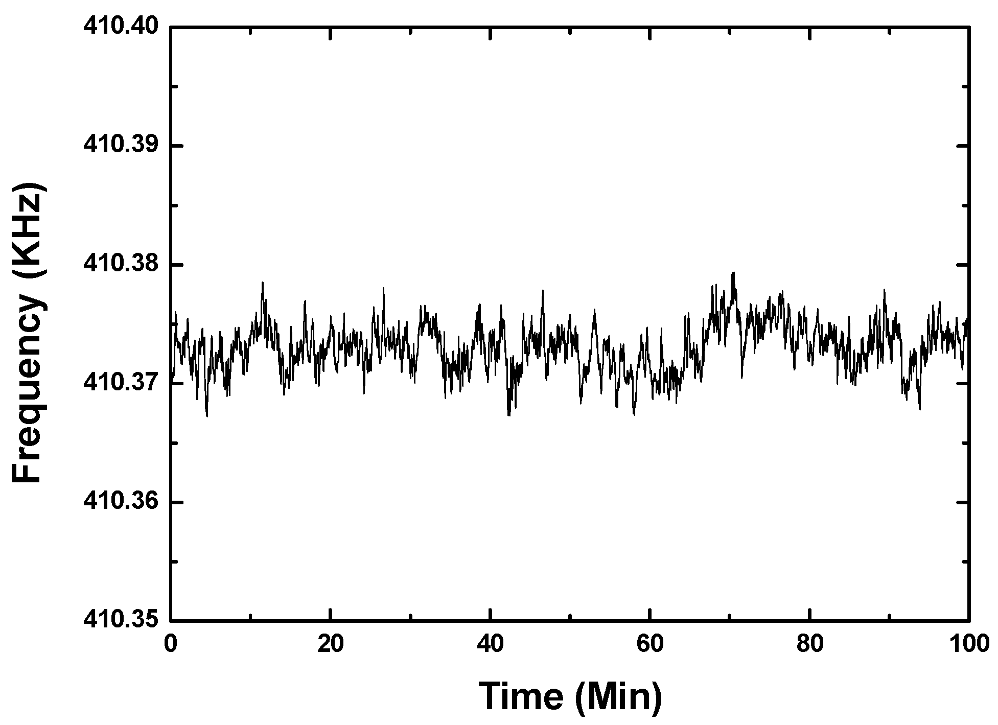
Prior to sensor performance evaluation, the baseline noise of the develop sensor was tested by measuring the frequency stability of the differential oscillator, as shown in Figure 11. Excellent short-term frequency stability of ±0.5 Hz/s and medium-term frequency stability of ±5 Hz/h were obtained.
4.3. Hysteresis Measurement
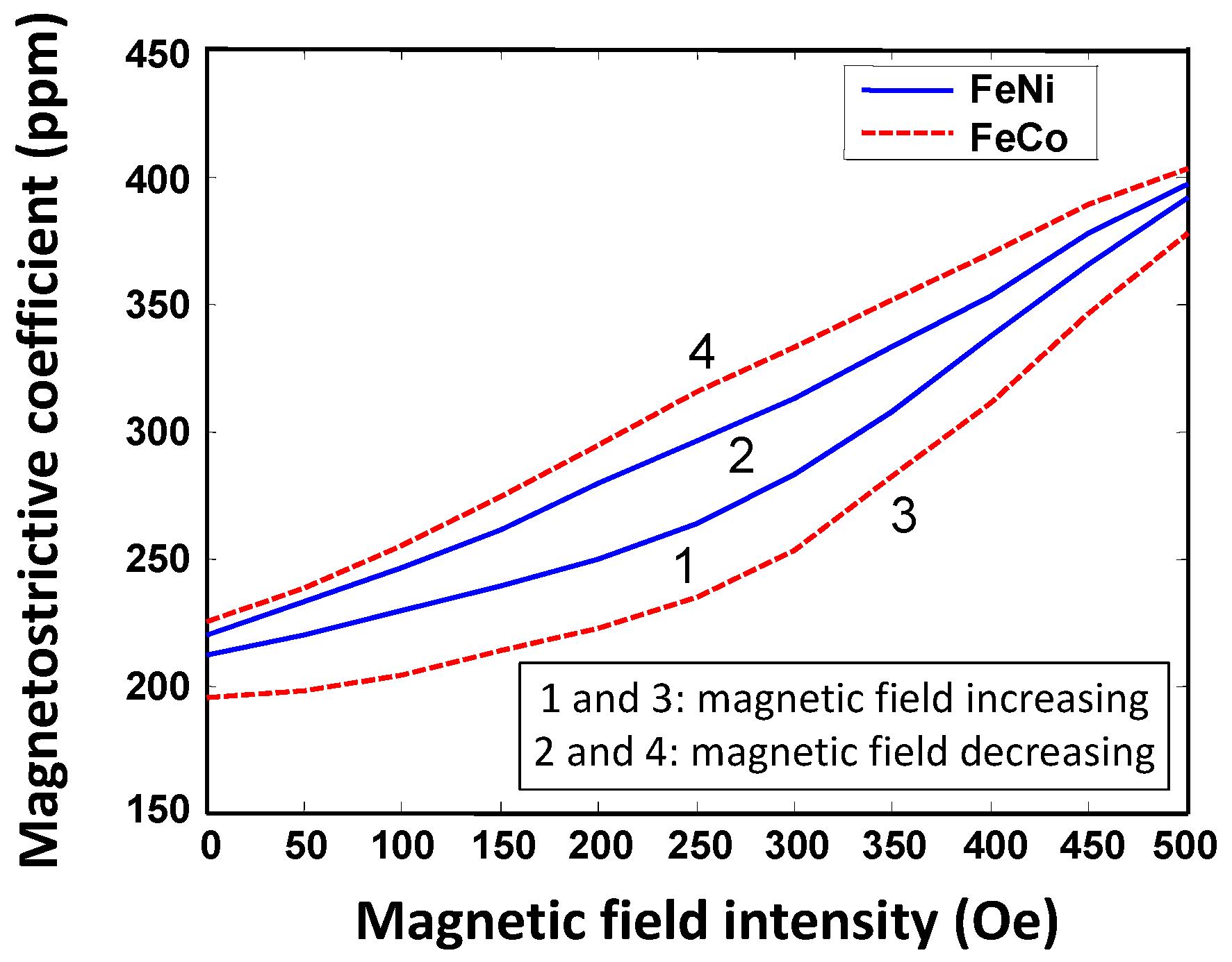
The hysteresis loops of the FeNi and FeCo were characterized by using the resistance strain gauge method [20], as depicted in Figure 12. The horizontal and vertical axes in the graph stand for external magnetic field intensity and magnetostrictive coefficient respectively. The curves 1 and 2 represent the corresponding changes in the magnetostriction of the FeNi coating at increasing and decreasing magnetic field intensity, respectively. Meanwhile, the curves 3 and 4 characterize the relationship between the magnetostrictive coefficient of the FeCo and the external magnetic field. It is clear that the hysteresis loop of FeNi and FeCo were distinctly different. Owing to the week remanence and hysteresis effect, the FeNi alloy exhibits relatively narrow and steep hysteresis loop over the FeCo, which means the FeNi coated sensor will offer better symmetry in current sensing. That is the reason why the FeNi was favored as the magneticsensitive interface for magnetic sensing.
4.4. FeNi Film Thickness and Aspect Ratio Effect on Sensor Performance
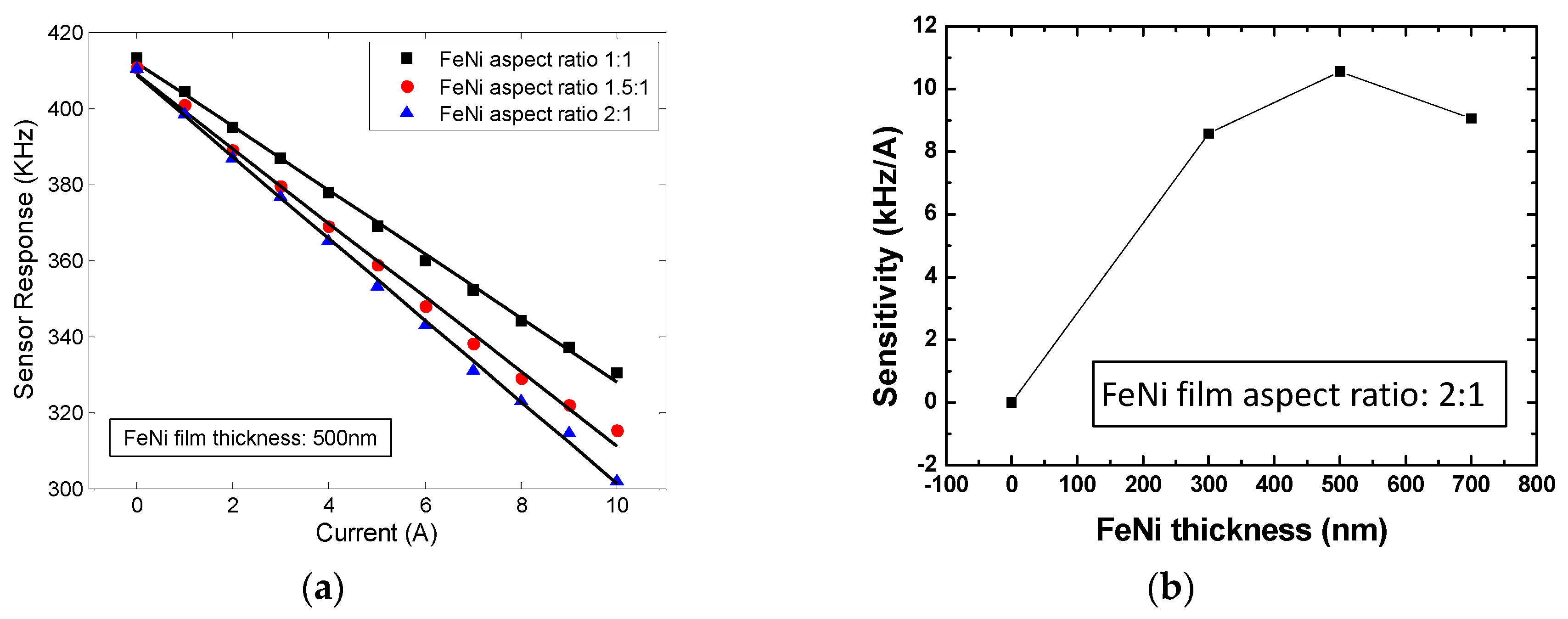
The sensor response of the developed 150 MHz SAW sensors with different FeNi film aspect ratio (1:1, 1.5:1, and 2:1) and various FeNi film thickness (300, 500, and 700 nm) were characterized at current range of 0~10 A and room temperature (20 °C), as concluded in Figure 13. Figure 13a indicates the sensor sensitivity for different FeNi film aspect ratio (1:1, 1.5:1, and 2:1) was measured to be 8.4, 9.7, and 10.7 KHz/A. Obviously, larger aspect ratio of FeNi film is effective to improve the sensor sensitivity. On the other hand, the effect on sensor sensitivity from the FeNi film thickness is relatively complicated, as shown in Figure 13b. Compared to the sensors with FeNi film thickness of 300 and 700 nm, the senor with a 500 nm thickness FeNi film has highest sensitivity, which agrees well with the calculated result mentioned in Figure 4a. Therefore, the optimal FeNi thickness and aspect ratio were determined to be ~500 nm and 2:1, respectively.
4.5. Repeatability Test
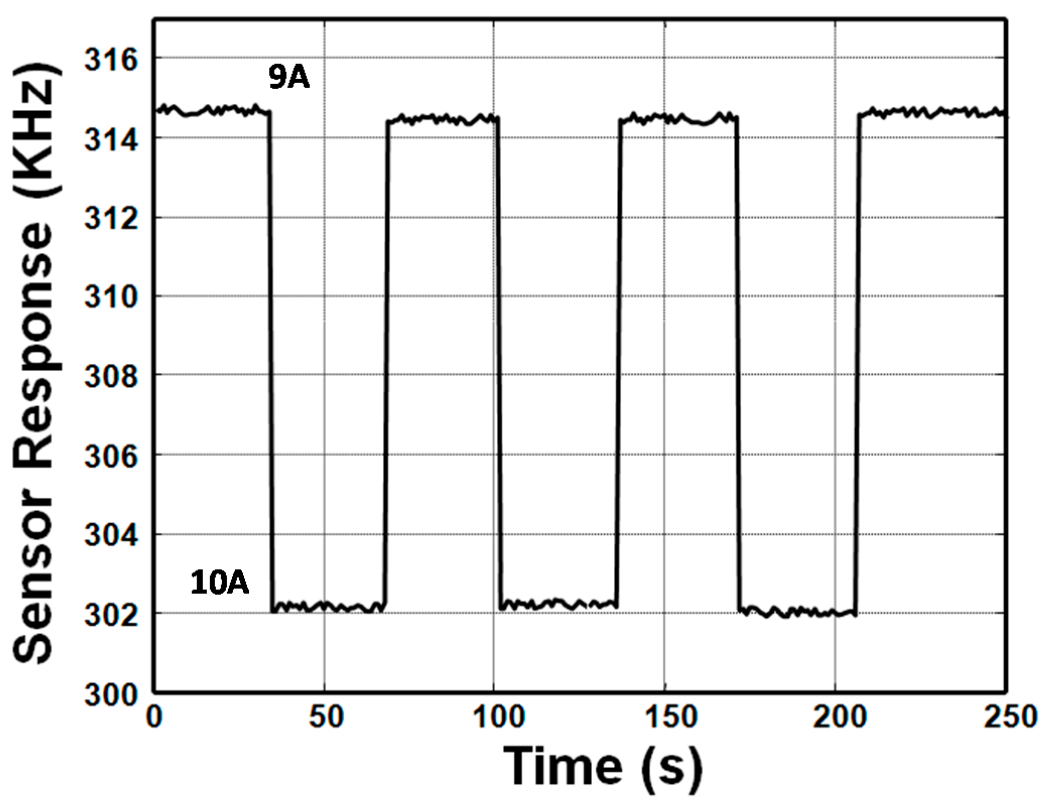
Response and recovery times for current sensing were tested by using the developed FeNi coated current sensor with FeNi aspect ratio of 2:1 and thickness of 500 nm. Sensor response measurements were performed for three consecutive 40-s exposures to current at intensity from 9 A to 10 A, as shown in Figure 14. When the current was varied from 9 A to 10 A, the frequency response showed a rapid rise (only one sampling point) to its steady-state value. When the current was decreased to 9 A, the frequency response rapidly fell to its initial value. From this promising result, we hypothesize that the developed sensor exhibits excellent repeatability and fast response.
4.6. Symmetry and Sensitivity Evaluation
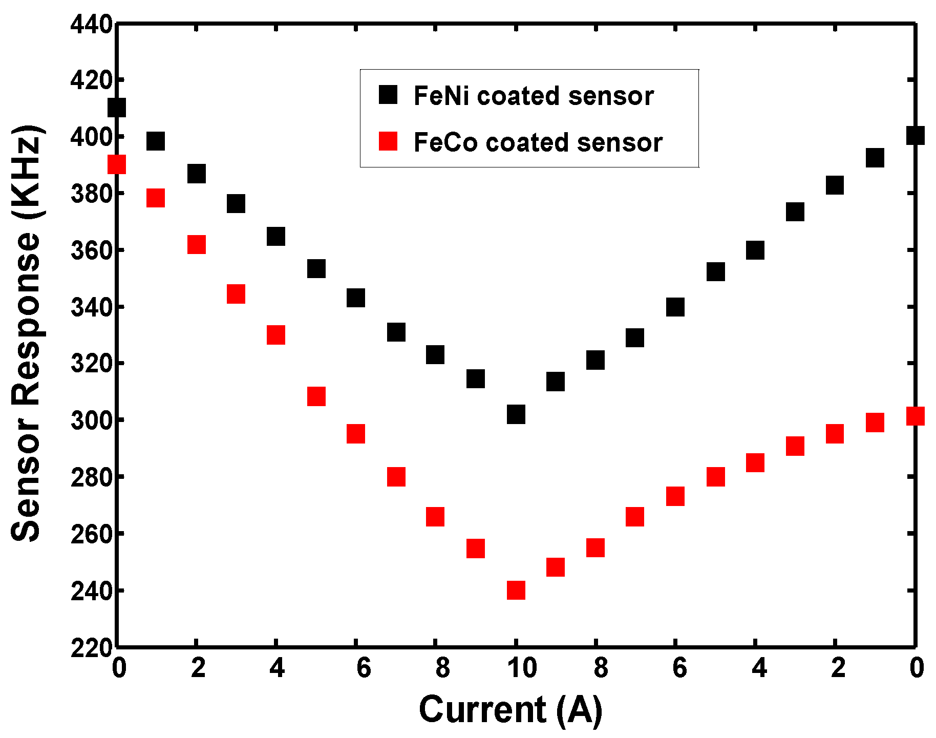
Then, the symmetry of the developed current sensor was the main concern in this work, and measured as shown in Figure 15. It is obviously that the gathered sensor signal decreases monotonically with increasing current intensity from 0 to 10 A, meanwhile, it increases with decreasing current intensity, and reaches to the initial value. It means that good symmetry in sensor response was observed for the FeNi coated current sensor.
Also, for comparison, the symmetry of the developed FeCo coated current sensor [12] was measured as shown in Figure 15. The obvious asymmetry phenomenon was observed in the sensor response at increasing and decreasing current intensity, which is caused by its larger remanence and hysteresis effect over the FeNi described in Figure 3.
Usually, the hysteresis error (εH) was defined by , , where yui and ydi are the response at the same current input when the current increases and decreases, yFS is the full-scale output of the current sensor. Hence, a hysteresis error of 0.97% was obtained from the FeNi coated sensor, which is substantially lower than the FeCo coated sensor (8.72%).
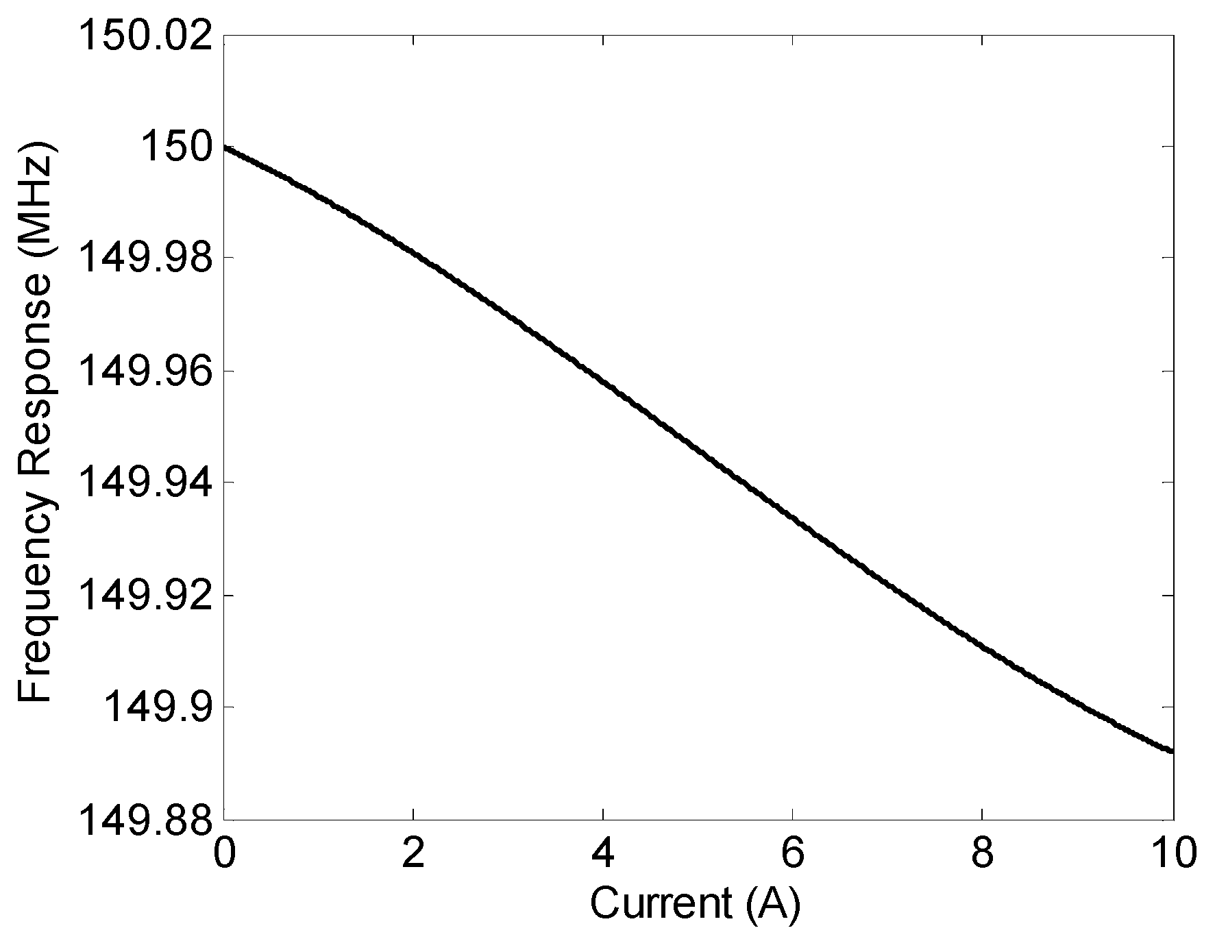
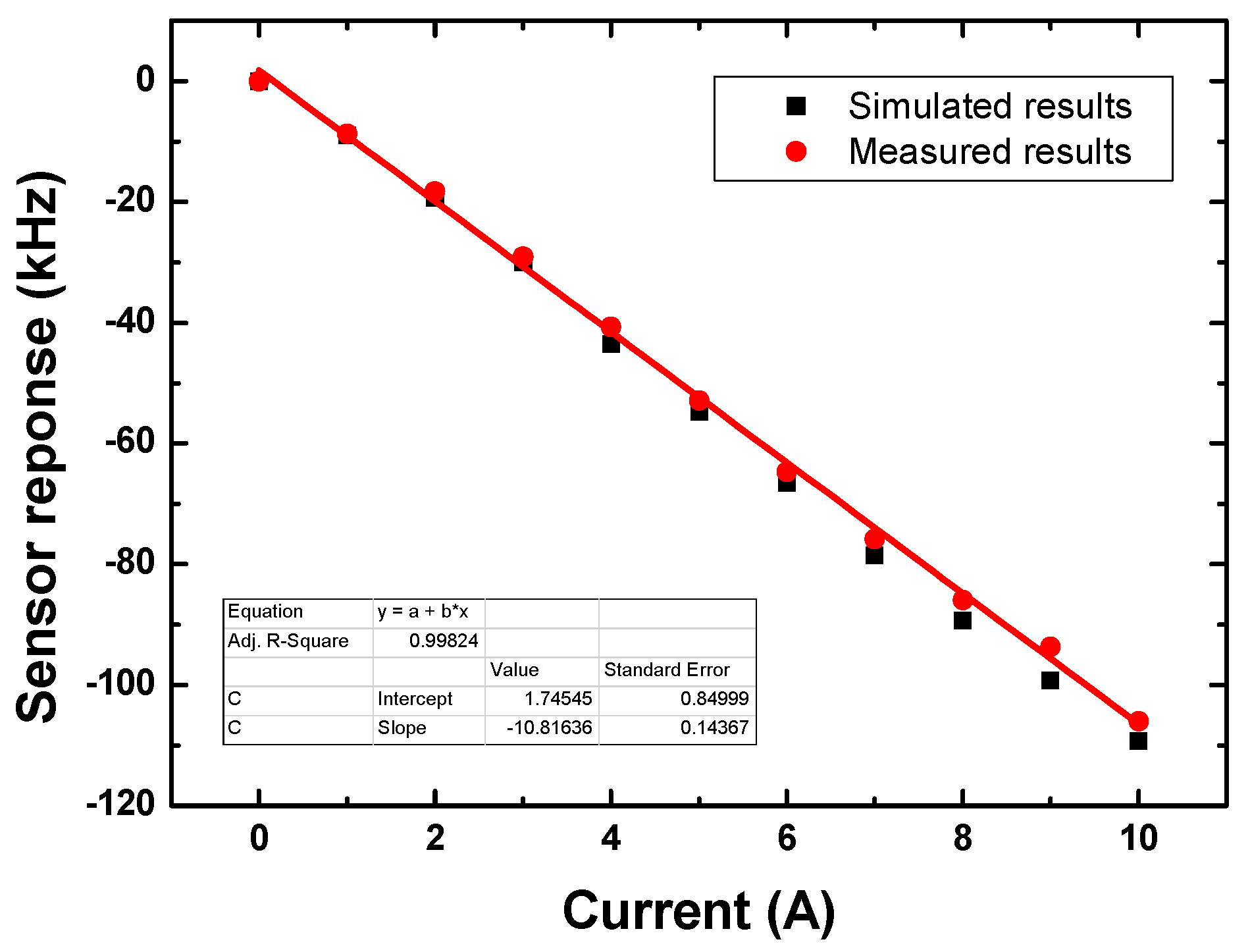
The corresponding sensitivity was measured to be 10.7 KHz/A, which agrees well with the predicted value of 11 KHz/A, as shown in Figure 16, and it corresponds to a magnetic field sensitivity of 5.35 KHz/Oe. Usually, the detection limit in current sensing closely relates to the frequency stability of the oscillator. Considering the measured short-term stability of ±0.5 Hz/s, and 10.8 KHz in response to current of 1 A, the threshold detection limit of the developed sensor was expected to be ~0.2 mA. From these results, we suggest that this prototype FeNi coated SAW sensor is very promising for current sensing with high sensitivity, excellent repeatability, good symmetry and linearity.
5. Conclusions
To improve the symmetry in sensor response, a magnetostrictive FeNi film was used to construct the SAW based current sensor. The optimal design parameters were determined theoretically prior to sensor development. High sensitivity of 10.7 KHz/A, low detection limit of 0.2 mA, excellent linearity of 1.22%, and lower hysteresis error of 0.97% in sensor response were achieved from the developed 150 MHz FeNi coated SAW current sensor, in which, the FeNi film thickness and aspect ratio was designed to 500 nm and 2:1, respectively.
Acknowledgments
This work was supported by National Natural Science Foundation of China (No. 11374254) and technological project of State Grid Corporation of China (DG71-15-038/5442DG150031).
Author Contributions
Jie Tong and Wen Wang conceived and designed the experiments; Yana Jia designed and fabricated the sensor chips; Yang Wang performed the experiments; Shiyue Wang conducted the experimental data analysis; Xinlu Liu performed the data collection; Yuqing Lei drew the figures; Wen Wang wrote the paper.
Conflicts of Interest
The authors declare no conflict of interest.
References
- Tang, Y.L.; Li, Z.J.; Ma, J.Y. Ammonia gas sensors based on ZnO/SiO2 bi-layer nanofilms on ST-cut quartz surface acoustic wave devices. Sens. Actuators B 2014, 201, 114–121. [Google Scholar] [CrossRef]
- Ji, X.; Fan, Y.; Chen, J.; Han, T.; Cai, P. Passive wireless torque sensor based on surface transverse wave. IEEE Sens. J. 2016, 16, 888–894. [Google Scholar] [CrossRef]
- Wang, W.; Huang, Y.; Liu, X.L.; Liang, Y. Surface acoustic wave acceleration sensor with high sensitivity incorporating ST-X quartz cantilever beam. Smart Mater. Struct. 2015, 24, 015015. [Google Scholar] [CrossRef]
- Ma, G.M.; Wu, Z.; Zhou, H.Y.; Jiang, J. A wireless and passive on-line temperature monitoring system for GIS based on surface acoustic wave sensor. IEEE Trans. Power Deliv. 2016, 31, 1270–1280. [Google Scholar] [CrossRef]
- Stoney, R.; Geraghty, D.; Odonnell, G.E. Characterization of differentially measured strain using passive wireless surface acoustic wave strain sensors. IEEE Sens. J. 2014, 14, 722–728. [Google Scholar] [CrossRef]
- Kadota, M.; Shigeo, I.; Yoshihiro, I.; Takuo, H.; Kenjiro, O. Magnetic sensor based on surface acoustic wave resonators. Jpn. J. Appl. Phys. 2011, 50, 07HD07. [Google Scholar] [CrossRef]
- Kadota, M.; Shigeo, I. Sensitivity of surface acoustic wave magnetic sensors composed of various Ni electrode structures. Jpn. J. Appl. Phys. 2012, 51, 07GC21. [Google Scholar] [CrossRef]
- Meriem, E.; Omar, E.; Abdelkrim, T.; Keltouma, A.A.; Laurent, B.; Frederic, S. FEM modeling of multilayer piezo-magnetic structure based surface acoustic wave devices for magnetic sensor. Procedia Eng. 2014, 87, 408–411. [Google Scholar]
- Meriem, E.; Omar, E.; Sebastien, P.W.; Laurent, B.; Sergei, Z. Magnetic field SAW sensors based on magnetostrictive-piezoelectric layered structures: FEM modeling and experimental validation. Sens. Actuators A Phys. 2016, 240, 41–49. [Google Scholar]
- Li, W.; Dhagat, P.; Jander, A. Surface acoustic wave magnetic sensor using galfenol thin film. IEEE Trans. Magn. 2012, 48, 4100–4102. [Google Scholar] [CrossRef]
- Zhou, H.; Talbi, A.; Tiercelin, N.; Matar, O.B. Multilayer magnetostrictive structure based surface acoustic wave devices. Appl. Phys. Lett. 2014, 104, 114101. [Google Scholar] [CrossRef]
- Wang, W.; Jia, Y.; Liu, X. Enhanced sensitivity of temperature-compensated SAW based current sensor using the magnetostrictive effect. Smart Mater. Struct. 2017, 26, 025008. [Google Scholar] [CrossRef]
- Hauser, H.; Steindl, R.; Hausleitner, C.; Pohl, A.; Nicolics, J. Wirelessly interrogable magnetic field sensor utlizing giant magneto-impedance effect and surface acoustic wave devices. IEEE Trans. Instrum. Meas. 2000, 49, 648–652. [Google Scholar] [CrossRef]
- Li, B.; Morsy, A.M.; Kosel, J. Ooptimization of autonomous magnetic field sensor consisting of giant magnetoimpedance sensor and surface acoustic wave transducer. IEEE Trans. Magn. 2012, 48, 4324–4327. [Google Scholar] [CrossRef]
- Li, B.; Yassine, O.; Kosel, J. A surface acoustic wave passive and wireless sensor for magnetic fields, temperature, and humidity. IEEE Sens. J. 2015, 15, 453–462. [Google Scholar] [CrossRef]
- Steindl, R.; Hausleimer, C.; Hauser, H. Wireless magnetic field sensor employing SAW-transponder. In Proceedings of the 2000 12th IEEE International Symposium on Applications of Ferroelectrics 2000 (ISAF 2000), Honolulu, HI, USA, 21 July–2 August 2000; pp. 855–858. [Google Scholar]
- Reindl, L. Wireless Passive SAW Identification Marks and Sensors. In Proceedings of the 2nd International Symposium Acoustic Wave Devices for Future Mobile Communication Systems, Chiba, Japan, 3–5 March 2004; pp. 1–12. [Google Scholar]
- Wang, W.; He, S.; Li, S. Enhanced Sensitivity of SAW Gas Sensor Coated Molecularly Imprinted Polymer Incorporating High Frequency Stability Oscillator. Sens. Actuators B Chem. 2007, 125, 422–427. [Google Scholar]
- Plessky, V.P.; Koskela, J. Coupling-of-modes analysis of SAW devices. Int. J. High Speed Electr. Syst. 2000, 10, 1–81. [Google Scholar] [CrossRef]
- Auckenthaler, R.; Carey, M.; Lioy-Thomas, H. Score normalization for text-independent speaker verification systems. Digit. Signal Process. 2000, 10, 42–54. [Google Scholar] [CrossRef]
- Auld, B.A. Acoustic Fields and Waves in Solids; Wiley: New York, NY, USA, 1973; Volume 1. [Google Scholar]
- Milsom, R.F.; Reilly, N.; Redwood, M. Analysis ofgeneration and detection of surface and bulk acoustic waves by interdigital transducers. IEEE Trans. Sonics Ultrason. 1977, 24, 147–166. [Google Scholar] [CrossRef]
- Cao, D.; Jin, C.; Pan, L. Magnetic Properties and Microstructure Investigation of FeNi Films with Step-Height by Nano-MOKE. IEEE Trans. Magn. 2015, 51, 2005004. [Google Scholar] [CrossRef]
- Morales, A.L.; Nieto, A.J. Simultaneous Measurement of Young’s Modulus and Damping Dependence on Magnetic Fields by Laser Interferometry. In Proceedings of the International Conference on Thermal, Mechanical and Multi-Physics Simulation Experiments in Microelectronics and Micro-Systems, London, UK, 16–18 April 2007; pp. 1–5. [Google Scholar]
- Pyati, V.P. Simplified Biot-Savart Law for Planar Circuits. IEEE Trans. Educ. 1986, E-29, 32–33. [Google Scholar] [CrossRef]
Figure 1.
The scheme and working principle of the surface acoustic wave (SAW) current sensor.
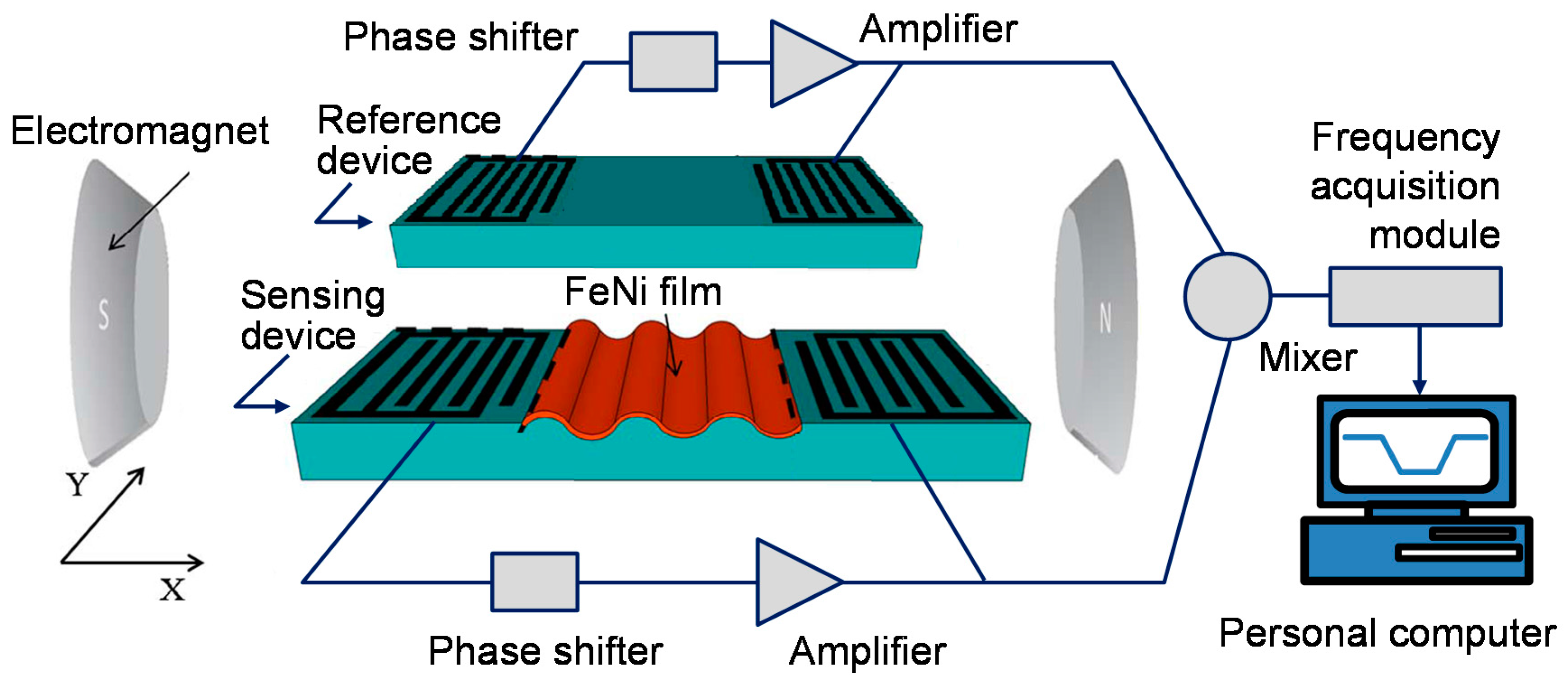
Figure 2.
The corresponding coordinate system in this work.
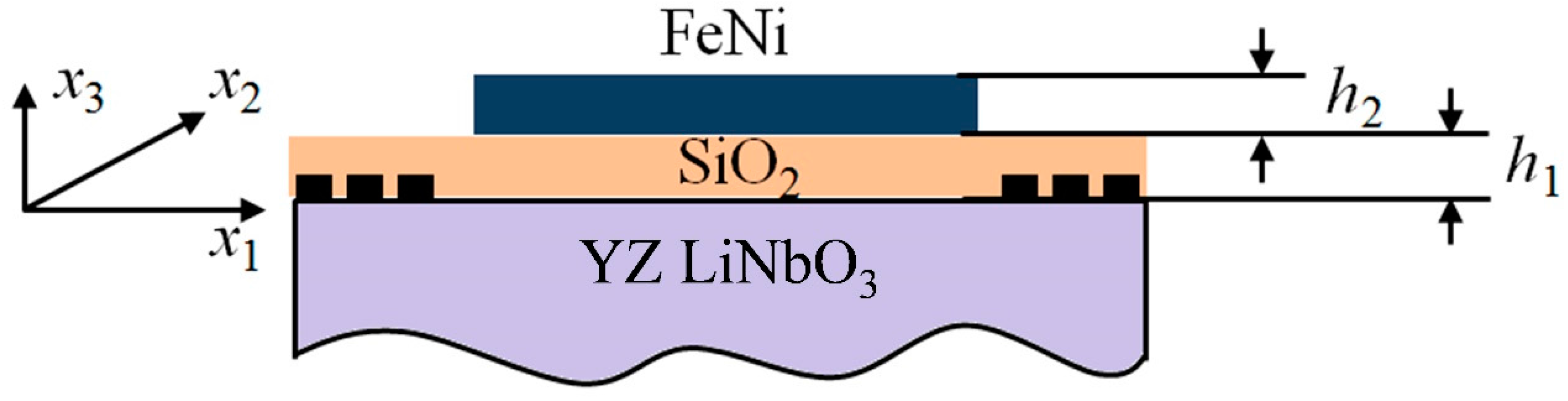
Figure 3.
Measured relationship between the young modulus of FeNi and magnetic field intensity.
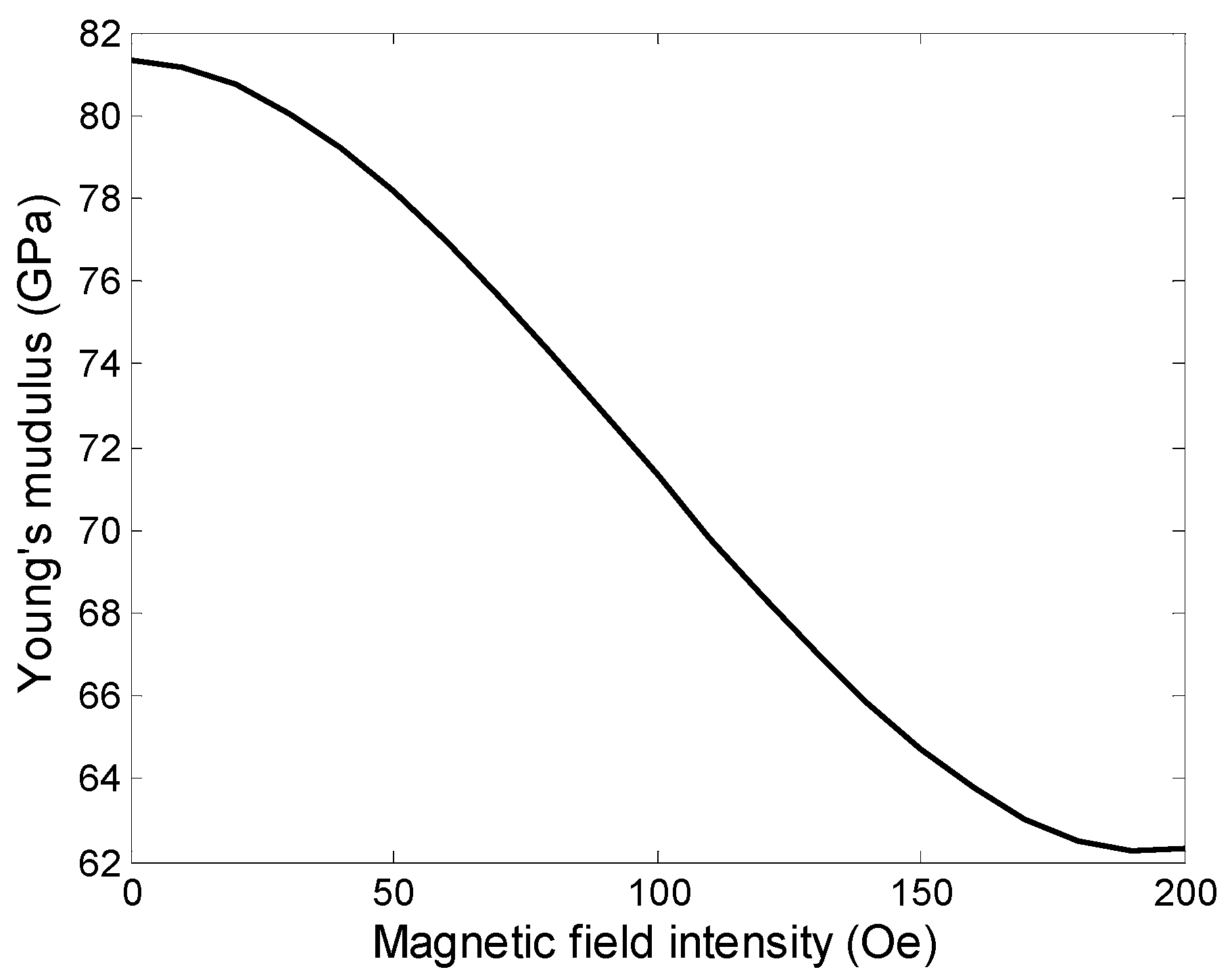
Figure 4.
The calculated relationship among the sensor response and the FeNi film thickness (a), and the aspect ratio (b), where the electromagnetic field intensity is set to 200 Oe.
Figure 4.
The calculated relationship among the sensor response and the FeNi film thickness (a), and the aspect ratio (b), where the electromagnetic field intensity is set to 200 Oe.
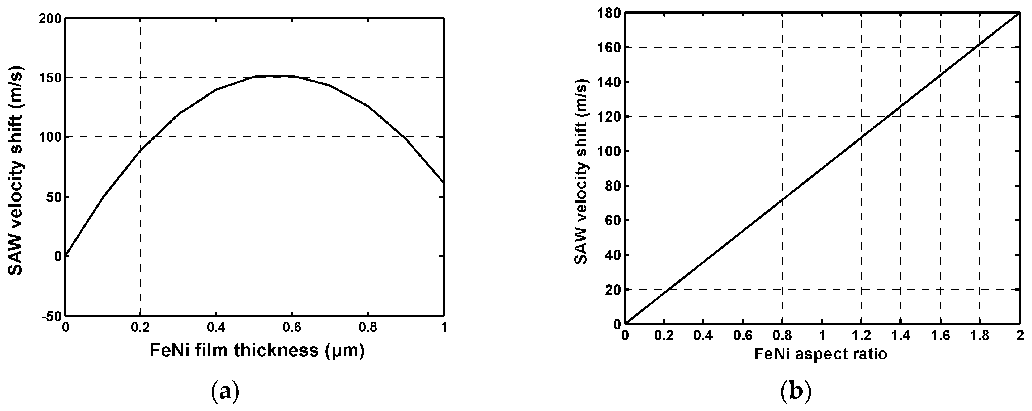
Figure 5.
The calculated sensor response of FeNi coated SAW current sensor.

Figure 6.
The technological process of SAW current sensor chip. IDT: interdigital transducer; PECVD: plasma enhanced chemical vapor deposition.
Figure 6.
The technological process of SAW current sensor chip. IDT: interdigital transducer; PECVD: plasma enhanced chemical vapor deposition.
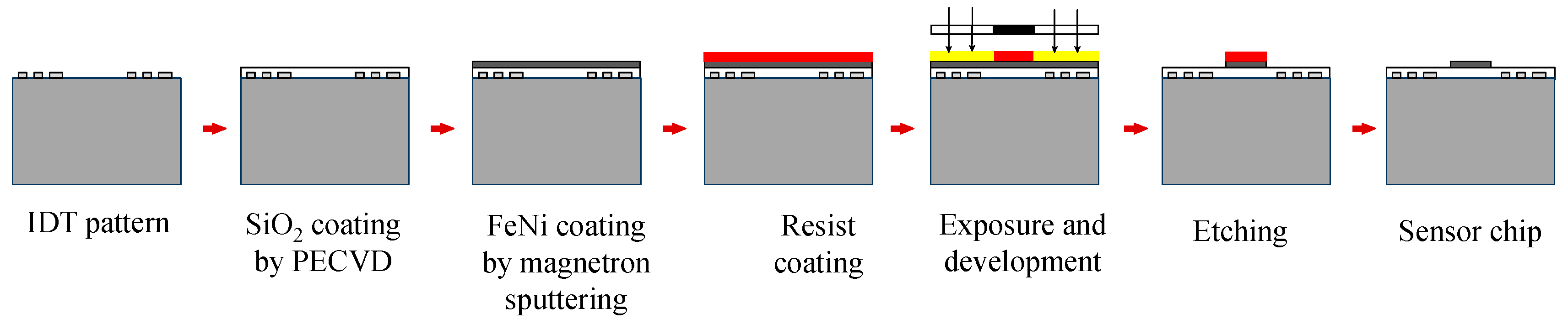
Figure 7.
The physical picture of developed sensor chip, FeNi thickness: 500 nm, aspect ratio: 1:1.
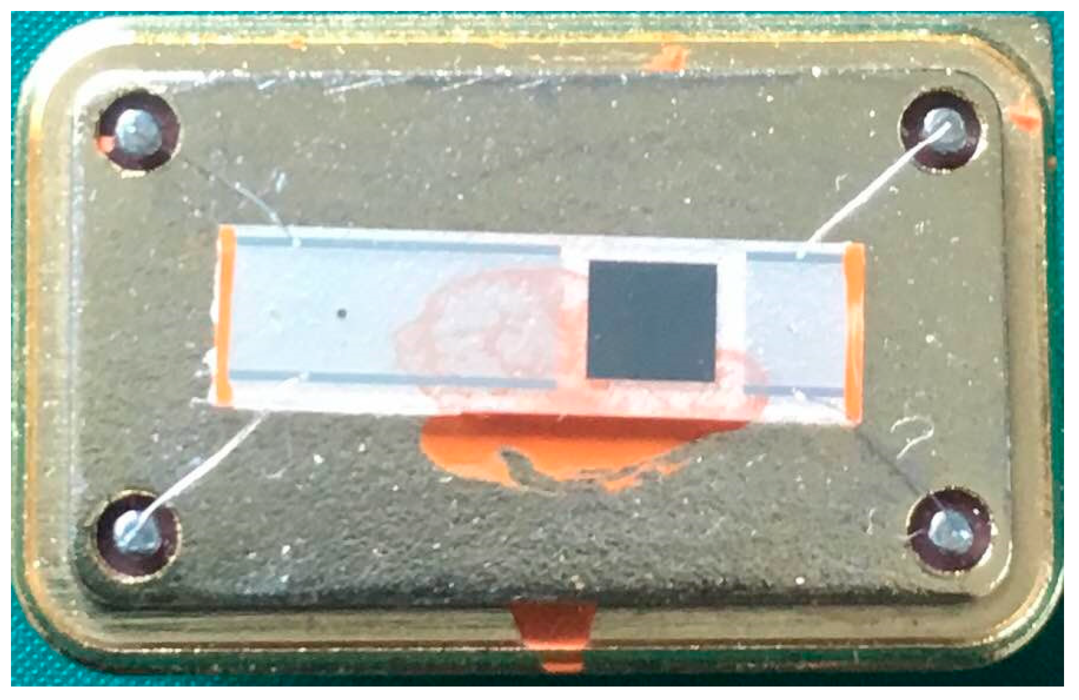
Figure 8.
The observed surface morphology of the FeNi coating.

Figure 9.
Measured frequency response of the FeNi coated sensor chip.
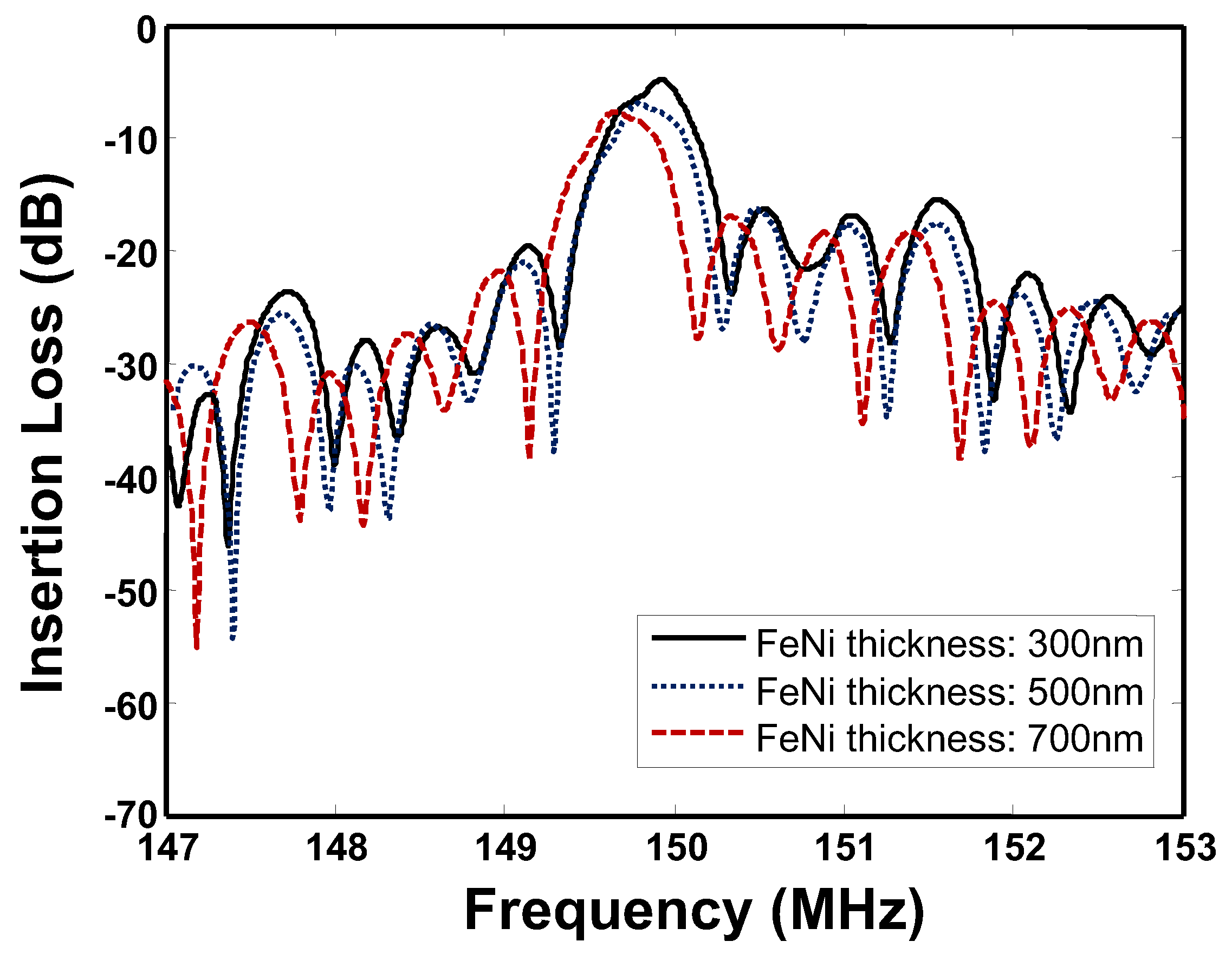
Figure 10.
The physical picture and schematic diagraph of the experimental setup for sensor performance evaluation, (a) experimental setup; (b) working principle.
Figure 10.
The physical picture and schematic diagraph of the experimental setup for sensor performance evaluation, (a) experimental setup; (b) working principle.

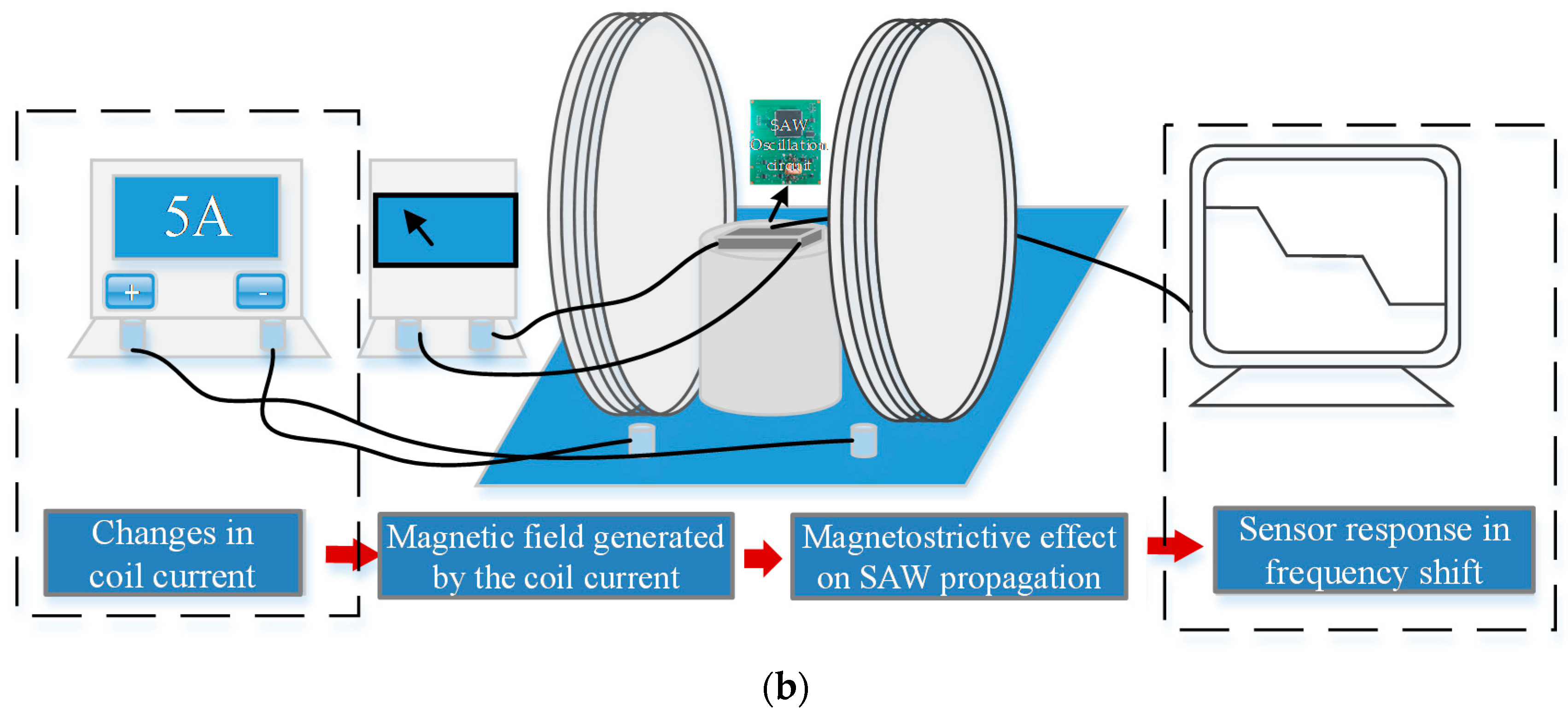
Figure 11.
The baseline noise measurement of the developed sensor.

Figure 12.
The measured magnetostrictive curves for FeCo and FeNi.

Figure 13.
The effect on sensor response from the FeNi aspect ratio (a) and FeNi thickness (b).

Figure 14.
The repeatability test of the developed SAW sensor.

Figure 15.
The symmetry test of the FeNi coated sensor and in comparison to FeCo coated sensor.

Figure 16.
The sensitivity evaluation of the developed FeNi coated sensor.


Table 1.
Physical parameters of the piezoelectric substrate, SiO2, and FeNi.
| Materials Parameters | Values | |||
|---|---|---|---|---|
| LiNbO3 | SiO2 | FeNi | ||
| Stiffness Coefficients (1011 N m−2) | C11 | 2.03 | 0.785 | 1.077 |
| C12 | 0.53 | 0.46 | ||
| C13 | 0.75 | |||
| C14 | 0.09 | |||
| C33 | 2.45 | |||
| C44 | 0.6 | 0.312 | 0.307 | |
| Piezoelectric Modules (C m−2) | e31 | 0.2 | ||
| e15 | 3.7 | |||
| e33 | 1.3 | |||
| e22 | 2.5 | |||
| Permittivity Constants (10−11 F m−1) | ε11 | 84 | ||
| ε33 | 29 | |||
| Density (kg/m3) | 7450 | 2651 | 8.38 | |
| Magnetostrictive Constant (10−6) | 400 | |||
| Young’s Modulus (109 N/m2) | 80 | |||
© 2017 by the authors. Licensee MDPI, Basel, Switzerland. This article is an open access article distributed under the terms and conditions of the Creative Commons Attribution (CC BY) license (http://creativecommons.org/licenses/by/4.0/).
Share and Cite
MDPI and ACS Style
Tong, J.; Jia, Y.; Wang, W.; Wang, Y.; Wang, S.; Liu, X.; Lei, Y. Development of a Magnetostrictive FeNi Coated Surface Acoustic Wave Current Sensor. Appl. Sci. 2017, 7, 755. https://doi.org/10.3390/app7080755
AMA Style
Tong J, Jia Y, Wang W, Wang Y, Wang S, Liu X, Lei Y. Development of a Magnetostrictive FeNi Coated Surface Acoustic Wave Current Sensor. Applied Sciences. 2017; 7(8):755. https://doi.org/10.3390/app7080755
Chicago/Turabian StyleTong, Jie, Yana Jia, Wen Wang, Yang Wang, Shiyue Wang, Xinlu Liu, and Yuqing Lei. 2017. "Development of a Magnetostrictive FeNi Coated Surface Acoustic Wave Current Sensor" Applied Sciences 7, no. 8: 755. https://doi.org/10.3390/app7080755
Note that from the first issue of 2016, this journal uses article numbers instead of page numbers. See further details here.