Review

Toward Defect Engineering Strategies to Optimize Energy and Electronic Materials

1
Section of Solid State Physics, University of Athens, Panepistimiopolis Zografos, Athens 15784, Greece
2
Department of Mechanical Engineering, Piraeus University of Applied Sciences, Athens 12241, Greece
3
School of Physics, V. N. Karazin Kharkiv National University, 4 Svobody sq., Kharkiv 61000, Ukraine
4
Faculty of Engineering and Computing, Coventry University, Priory Street, Coventry CV1 5FB, UK
5
Department of Materials, Imperial College London, London SW7 2BP, UK
*
Author to whom correspondence should be addressed.
Appl. Sci. 2017, 7(7), 674; https://doi.org/10.3390/app7070674
Submission received: 3 June 2017 / Revised: 23 June 2017 / Accepted: 27 June 2017 / Published: 30 June 2017
(This article belongs to the Section Materials Science and Engineering)

Abstract

:
The technological requirement to optimize materials for energy and electronic materials has led to the use of defect engineering strategies. These strategies take advantage of the impact of composition, disorder, structure, and mechanical strain on the material properties. In the present review, we highlight key strategies presently employed or considered to tune the properties of energy and electronic materials. We consider examples from electronic materials (silicon and germanium), photocatalysis (titanium oxide), solid oxide fuel cells (cerium oxide), and nuclear materials (nanocomposites).

1. Introduction

In the past few decades of the miniaturization of devices, the introduction of more structurally complicated materials in conjunction with demanding processing and operating conditions have made the study of defects in materials increasingly important [1,2,3,4,5,6,7,8,9,10]. There is no single recipe of how to treat materials and what is the optimum concentration of defects. In a material, some defects and dopants can have a beneficial impact and in a similar material the same defects can deteriorate its physical properties. For example, n-type dopants in silicon are necessary to form devices and do not readily interact with vacancies due to the low concentration of the latter. In isostructural germanium, n-type dopants are hard to contain as they diffuse aided by vacancies and it is hard to form n-doped regions [3]. The same arguments can apply to energy related materials (for example nuclear, fuel cell, and battery materials) for which there is presently a requirement to employ and/or form materials with better properties that will need to operate at more difficult conditions for longer periods of time.
Using defect engineering strategies is an efficient way to tune the physical properties and optimize materials for energy and electronic applications. Defect engineering strategies in essence use the differences that composition, structure, disorder, and strain can have on the physical properties of the material. It is impossible to highlight all the progress in the field and contain it in a single review. In the present review, we consider a range of applications and materials from nanocomposites to more traditional systems such as silicon and titanium dioxide aiming to demonstrate how the defect engineering strategies considered can be transferable to numerous systems and applications.

2. Advanced Materials for Nuclear Applications

2.1. Background

About 70 years since Enrico Fermi et al. built the first nuclear reactor, nuclear power is once more in the spotlight. There is a need for the new generation of safer and more proliferation resistant reactors whose introduction would have the beneficial effect of lowering CO2 emissions due to electricity generation. Several high profile nuclear incidents have cast a shadow over the nuclear industry in the past. As a consequence, for nuclear power generation to have a bright future it will be necessary to allay fears regarding safety, proliferation, and the long term management of wastes. This, together with institutional inertia and the cost to develop new nuclear technologies may delay its progress. Atomic scale simulation techniques can accelerate the development of new nuclear materials and provide detailed information on their physical properties that cannot be easily assessed by experiments.
Nuclear energy is potentially important for the future energy mix given the need to address the increasing global energy demand and simultaneously reduce CO2 emissions [11,12,13,14,15]. Nuclear materials are subjected to extreme conditions and the detailed understanding of their properties often at the atomistic scale is necessary to ensure their high performance and more importantly their safety. The ever increasing computational power has allowed the investigation of the behaviour of nuclear materials with atomistic modeling techniques that were not available when most commercial reactors operating today were designed.
The efficiency of nuclear reactors can be increased via higher operating temperatures, increasing their lifetime and taking fuels to higher burn-ups. Additionally, the introduction of new materials such as thorium dioxide (ThO2) or mixed oxide based nuclear fuels requires extensive investigation prior to their use in nuclear reactors [13]. The evolution of nuclear material properties under a range of conditions encountered in the harsh environments in which they operate can be a challenge for scientists.
Nuclear fission was observed in 1939 by Otto Hahn and Fritz Strassman. Following the bombardment of uranium with neutrons, they discovered two products with lighter nuclei, barium and lanthanum. Thereafter, Lise Meitner and Otto Frisch explained the phenomenon that is presently exploited in nuclear reactors to generate heat. This heat is in turn used to heat water into pressurized steam, which runs through turbines powering electrical generators.
Nuclear energy is acknowledged as a key component of the mix of energy sources to reduce greenhouse gas emissions and the dependence on fossil fuel. A main advantage of nuclear energy is its high energy density; that is, the quantity of energy derived from nuclear fuel is orders of magnitude larger than competitive energy sources such as fossil fuels. The nuclear facilities are rather compact and require far less land as compared with solar energy on wind energy installations producing the same power. Nuclear power has been an established and reliable source of electricity in numerous countries (for example, USA, France, UK, Russia, China) for many decades. The possibility of hydrogen production via an efficient centralised technology taking advantage of mainly off-peak electricity production is another possibility. Taking into consideration that there are still substantial reserves of uranium and that alternative fuels can also be used (thorium-based) there should be enough nuclear fuel for many decades.
There are also negative issues with nuclear energy associated with the negative public perception stemming from nuclear accidents, nuclear waste management, and proliferation issues. Nuclear accidents (for example Three Mile Island, Chernobyl, and Fukushima) have dealt a major blow to the nuclear industry and its reputation. Although nuclear energy results in far less casualties than other forms of energy generation, it is considered to be very perilous. This is due to some examples of poor nuclear waste management, its association with nuclear weapons, and the long half-life of extremely radiotoxic nuclear waste.
To design and construct safer nuclear reactors for the coming decades, it is imperative to manufacture better nuclear materials. In particular, there is the requirement for radiation tolerant materials to store nuclear waste, advanced structural materials, and novel nuclear fuels.

2.2. Radiation Tolerant Materials

The safe storage of nuclear waste is considered as a prerequisite for public support. The construction of new reactors differs as compared to previous generations in that nuclear waste solutions including packaging materials and appropriate repositories must be thought of and identified as part of the initial design [16].
Nuclear waste management is a very difficult task due to the radiotoxicity and long half-lives of actinides and fission products. A feasible solution is to move nuclear waste to relatively stable geological formations. These repositories will be reinforced by barriers, for example corrosion-resistant cladding and compacted clay [17,18]. Identifying waste-packaging materials to host high-level waste (HLW) is difficult due to their decay production and the formation of point defects. In essence, these will eventually destabilize the host crystalline oxides resulting in their amorphization and cracking.
Nuclear materials operate at extreme conditions. To host nuclear waste, numerous systems have been investigated using both experimental and computer simulation techniques [19]. The synergetic application of techniques leads to the more thorough fundamental understanding of the impact of radiation damage in materials and can lead to progress. An example is by Sickafus et al. [19], which determined that radiation tolerance in pyrochlore oxides (A2B2O7) is related to the ease with which that disorder can be accommodated. Previous work determined that oxides were defects that can readily form and are more resistant to radiation-induced amorphization and are thus important for the accommodation of radioactive waste [19].
Inspired by nanotechnology, there has been interest in annihilating defects and radiation damage through the use of nanocomposites. This is a new class of radiation tolerant materials with nanometres thick layers (i.e., maximization of interfaces) that can lead to very radiation resistant materials. An example is the studies of Demkowicz et al. [20] on the radiation damage resistance in Cu-Nb multilayer nanocomposites (Figure 1). In this system, it was predicted using atomistic simulation that the interfaces in the nanocomposite effectively act as sinks for radiation-induced defects. As a word of caution, however, the application of finer grain wasteform materials will be a challenge due to the increased surface/area per unit volume that is thermodynamically less stable. This can be potentially problematic at the extended repository timescales.
In the recent work of Bai et al. [21], atomistic simulation was used to show that grain boundaries are not only sinks for radiation induced defects but can also emit interstitial atoms which can recombine with vacancies. This is considered to be important as it leads to concepts where grain boundaries will heal radiation-induced damage [21]. This is a breakthrough as the design principles relied on materials that could resist radiation damage, tolerate damage, or undergo lattice recovery. This is a further example of how nanotechnology can be used to produce designed grain-boundaries or interfacial structures to create advanced radiation tolerant materials.

3. Defect Engineering Oxygen Diffusion in Ceria

3.1. Motivation

The importance of solid oxide fuel cells (SOFCs) lies in their potential for high efficiency energy conversion in conjunction with the reduced emission of greenhouse gases [22,23]. The high temperatures (up to 1000 °C) that SOFCs operate at to convert hydrogen and/or natural gas chemical energy to electricity can be detrimental for materials (for example thermal cycling and performance degradation), leading to increased cost [24,25]. Lowering the operating temperature (i.e., to 500–700 °C) will be beneficial for material stability, however, it can also lead to increased losses for the reaction and transport kinetics in the cathode and electrolyte parts of the SOFC. A way to do this is to move away from traditional SOFC electrolyte materials such as yttria stabilised zirconia (YSZ) and towards materials such as rare-earth doped CeO2 that exhibit high oxygen self-diffusivities at these lower temperatures. Higher diffusivities are important for accelerating the oxygen transport in the electrolyte.

3.2. Doping and Strain Strategies

Oxygen self-diffusion in ceria is mediated by oxygen vacancies. Under equilibrium conditions the oxygen vacancy formation energy is high. A way to introduce oxygen vacancies to form an oxygen deficient structure is via doping with trivalent cations. Trivalent cations can substitute at cerium lattice sites with the defect equation in Kröger Vink notation being expressed as:
X 2 O 3 CeO 2 2 X Ce + V O ˙ ˙ + 3 O O X
Every oxygen vacancy is charge compensated by two trivalent ions that are introduced into the cation sublattice.
Trivalent doping in ceria is an efficient strategy leading to a SOFC electrolyte material with high oxygen ion diffusivity (for example, 2–3 orders of magnitude higher diffusivity as compared to yttria stabilized zirconia) in conjunction with relatively lower reduction temperatures [23]. In a previous molecular dynamics (MD) study [26], the activation energies of the oxygen migration of rare-earth doped ceria (Ce0.9R0.1O1.95 where R = Yb, Er, Ho, Dy, Gd, Sm, Nd, and La) as a function of the dopant ionic radius were considered (black line of Figure 2). The molecular dynamics calculations revealed that Nd-doped ceria had the lowest activation energy of oxygen migration (refer to Figure 2) [26]. This is reflected also in the oxygen diffusivities and therefore Nd-doped ceria is appropriate for intermediate temperature (500–700 °C) SOFCs. It should be stressed, however, that at very high temperatures the energy barrier for oxygen diffusion is not significantly impacted by the association energy (Coulombic interactions and relaxation of the ceria lattice) of the dopant-oxygen vacancy clusters [26,27].
The community also imposes strain to increase oxygen diffusion and other physical properties in metal oxides [26,28]. From an experimental viewpoint, strain can be introduced by the formation of interfaces between dissimilar oxides and due to the complexity, atomistic simulation is commonly used to gain insights [29]. The advantage of computational modeling techniques is that they can be employed to deconvolute different contributions so that it becomes clear how strain impacts defect processes such as oxygen diffusion. This is essential in order to gain an understanding of the effect of strain and to be able to tune and optimize strain fields to achieve enhanced oxygen diffusion (Figure 3). Strain fields can be introduced (a) locally via doping with isovalent atoms or (b) by the formation of heterostructures resulting in epitaxial strain fields mainly near the interface between the layers of the dissimilar materials [30,31,32]. Interestingly, the work of Garcia-Barriocanal et al. [33] determined up to an eight order-of-magnitude increase in conductivity for epitaxially-grown zirconia/strontium titanate heterostructures and this motivated the community [26,34]. To clarify this unprecedented result, numerous atomistic simulation studies were employed given that in these it is easier to employ and control strain as compared to the experiment [26,34].
At any rate, the accuracy of molecular dynamics simulations to describe oxygen diffusion in doped ceria will depend upon the potential model that should appropriately describe the thermal expansion of doped CeO2. For example, MD calculations were previously employed to study the effect of uniaxial strain on the oxygen ion diffusivity as a function of temperature and rare-earth dopant (Yb, Er, Ho, Dy, Gd, Sm, Nd and La) using the well-established Cooper-Rushton-Grimes potential model that appropriately describes the thermal expansion of doped ceria [26]. This MD study is consistent with an increase of the oxygen diffusion coefficient due to strain, but not of the same order of magnitude as the study of Garcia-Barriocanal et al. [32] inferred. Given the flexibility of MD calculations to change conditions, it was shown that the increase in temperature will result in the decrease in the difference between the diffusivities between the dopants [26]. This in essence illustrates the diminishing impact of the association between the dopants and the oxygen vacancies [26]. Therefore, at temperatures above 1000 K, the activation energy of oxygen migration will be primarily represented by the energy barrier required for diffusion, whereas the association energy of oxygen vacancy-dopant clusters will have a smaller contribution [35,36,37].
A very interesting feature that was demonstrated by the MD calculations for undoped CeO2 is that there is a limited increase of the oxygen diffusion coefficient for strains below 3% but there is a 15-fold increase in the oxygen diffusion coefficient as the strain increased from 3.0% to 5.0% (refer to Figure 4) [26]. This in essence demonstrates that the strain not only impacts the association of dopants with the oxygen vacancies, but also leads to changes in the oxygen diffusivity because of the changes in the lattice.

4. Doping Strategies in Silicon and Germanium

4.1. Isovalent Doping in Silicon

For numerous years silicon has been the dominant electronic material in the semiconductor industry. This has been achieved by its beneficial material properties and the versatile silicon dioxide that allowed for the efficient miniaturization of microelectronic devices. Silicon dioxide has better properties and is more stable than germanium dioxide and this has allowed silicon to prevail over germanium at the dawn of the semiconductor industry, although the first transistor was made of germanium.
Isovalent doping in Si is technologically important (i.e., photovoltaics) and it can be used to improve the radiation hardness of Si [38]. In particular, it was previously determined that isovalent doping can suppress the formation of oxygen- and carbon-related radiation defects in Si, thus allowing its application in photovoltaics [38]. The key is to immobilize vacancies as it is the key component of the vacancy-oxygen pair (VO or A-center) [39,40,41]. With the incorporation of large isovalent codopants in the silicon, elastic strains are induced around the defects due to the larger tetrahedral covalent radii of the dopants as compared to that of the host atom. These strains can be relieved by the attraction of a vacancy that in essence provides space for the lattice and the dopant to relax [38].
Sn is an isovalent dopant that is considerably larger than Si, so it can strongly bind with vacancies and thus it can influence the vacancy-related defects and the generation rate of interstitial-related defects [42,43,44,45]. It was previously determined that Sn doping and in particular high concentration Sn doping will significantly impact the formation and diffusion of A-centers in Si (refer to Figure 5) [39,40,41,46]. The key is the formation of the highly bound SnVO clusters, which are far less mobile than VO [47]. Alongside SnVO clusters, SnV and SnCi defects may also form in irradiated Si [48]. The main purpose to introduce Sn atoms is to capture vacancies and consequently to improve the radiation hardness of Si in applications where this is required (for example, solar cells and detectors) [38]. This is because less vacancies will be unbound and available to form vacancy-related defects such as VO, VO2, and PV (in n-type doped Si), which will have a deleterious impact on the output and reliability of devices [38]. Sn doping can also influence the generation of oxygen thermal donors, and the aggregation and precipitation processes in Si. At any rate, however, the SnV defect induces electrical levels in the gap [49,50,51].

4.2. Fluorine Doping in Germanium

The introduction of alternative oxides in microelectronics and in particular high dielectric constant oxides (high-k dielectrics such as hafnium oxide) has allowed the consideration of alternative substrates including germanium and III-V compounds [52,53,54,55]. Although Ge is isostructural to Si, its defect processes were considerably different and relatively neglected up until a decade ago [56,57,58]. The main issue that needs to be considered in Ge is the excessive n-type dopant diffusion, which can be significant as it is difficult to control so as to form appropriate n-type doped regions for devices.
A way to address this issue is via defect engineering strategies that can be employed to limit the harmful impact of defects, dopants, or their clusters in Ge (refer to Figure 6). A way to proceed is by the introduction of codopants or competing native defects at concentrations that will annihilate or control the defects, dopants, and their clusters. Bracht et al. [59] considered proton irradiation to form a supersaturation of Ge self-interstitials to annihilate the Ge vacancies. The formation of Ge interstitials is important as under equilibrium conditions, vacancies in Ge are the prevalent native point defects [3]. Vacancies mediate and are responsible for the fast diffusion of n-type dopants (P, As, or Sb) and the formation of large dopant-vacancy clusters (refer to Figure 6) that lead to the deactivation of a large proportion of the dopants introduced and therefore need to be controlled [60,61,62].
As in the case of Si, a more straightforward path towards the control of the defect processes in Ge is through the incorporation of codopants. Previous experimental and theoretical studies considered codoping of n-type doped Ge with isovalent atoms such as C or Sn, aliovalent dopants such as fluorine, or a second n-type dopant (double donor doping) [3]. Density functional theory (DFT) and experimental studies consistently revealed that isovalent codoping and double donor doping in Ge do not effectively reduce the formation of dopant-vacancy clusters that can lead to deactivation [63,64]. The introduction of fluorine in Si and Ge is motivated as it is a dopant that can passivate the dangling bonds formed by the vacancies [65,66,67,68,69,70]. The key is the high electronegativity of F and via the saturation of the dangling bonds, and it essentially immobilizes the lattice vacancies. This is important as the vacancies are the key to control both the diffusion of donor atoms and the formation of the large donor atom-vacancy clusters that lead to the deactivation of the donor profile. In a DFT study which employed mass action analysis, it was shown that F will more effectively capture vacancies (forming FnVm clusters) as compared to donor atoms and this will limit the concentration of the donor-vacancy clusters [68]. This theoretical study motivated Impellizzeri et al. [69] to investigate the effect of F on As diffusion in Ge. It was determined that F does reduce As diffusion in Ge (refer to Figure 7) [69]. Thereafter, the study of Jung et al. [70] was consistent and concluded that implanted F atoms can passivate the vacancies at around 500 °C leading to an enhancement in Ge-metal-oxide semiconductor-field-effect transistor (MOSFET) performance [70]. In a recent study, Sanson et al. [71] investigated the local structure of F doped Ge by ion implantation and annealing using X-ray absorption near edge structure (XANES) spectroscopy. This study determined that most of the F in Ge forms F6V2 complexes [71]. The excellent agreement of DFT and experiments to model F-doped Ge and the effectiveness of F to capture vacancies to form FnVm clusters demonstrates that their synergetic use leads to efficient defect engineering strategies that can accelerate the realization of advanced nanoelectronic devices [68,69,70,71,72,73].

5. Tuning Metal Oxides for Catalysis

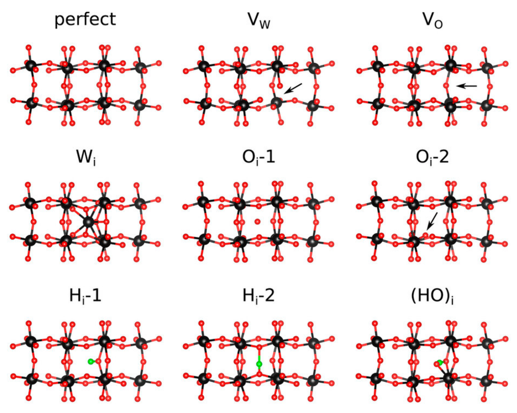
5.1. Hydrogen Doping in WO3

Tungsten oxide, WO3, can be used as a catalyst and catalyst support. To expand the range of applications to gas sensors and optoelectronics, it is necessary to control its intrinsic and/or extrinsic defect processes [74,75,76,77,78,79,80,81,82]. Importantly, although undoped and stoichiometric WO3 is insulating (band gap of 3–3.3 eV [76]), oxygen hypostoichiometric tungsten oxide has electrical conductivity and optical absorption (blue colour because of the gap narrowing) [78].
Hydrogen is an important dopant in metal oxides as it (a) can modify the band gap; (b) occupy interstitial sites with only limited distortion in the lattice; (c) induce insulator-to-conductor transitions; and (d) interact with intrinsic defects (for example, oxygen vacancies and interstitials) [76,79,80,81,82]. Understanding H doping and its impact in defect processes remains an active research area in many technologically important metal oxides including WO3 and TiO2.
Considering WO3, Zhu et al. [76] used DFT calculations to study the structure and formation of defects. Figure 8 represents the configurations of defects in WO3 reported in the study of Zhu et al. [76]. The calculations show that the O atoms that surround a W vacancy (VW) have only small distortions from their original positions, conversely to surrounding W atoms towards an O vacancy (VO) which exhibit significant distortions [76]. In WO3, the oxygen interstitials form at the body center (Oi-1) or at the vicinity of a W atom (Oi-2)—refer to Figure 8 [76]. The W interstitial (Wi) atom is stable at the body center having a larger bond length (W-O bond length of 2.08 Å) as compared to the perfect structure bond length (1.93 Å) [76]. Figure 8 represents the three possibilities for Hi: (a) bond to a single O atom (O-H distance of 0.98 Å, Hi-1); (b) be located at the face center (O-H distances of 1.01 Å and 1.67 Å, Hi-2); and (c) form the (HO)i interstitial defect (O-H distances of 1.02 Å and 1.50 Å) [76].
Figure 9 reports the formation energies of intrinsic and H-related defects in WO3 with respect to the Fermi level (O-rich and O-poor limits) for a range of charge states [76]. It can be observed that at the O-poor limit, the formation energy of VO is much lower as compared to VW and even negative for most of the values of the Fermi level (refer to Figure 8) [76]. For the O-rich limit, when the Fermi level is high, VW becomes more energetically favourable compared to VO [76]. For the oxygen interstitial defects, the formation energy of Oi-1 is higher than that of Oi-2 (refer to Figure 8 for the configurations and Figure 9 for the formation energies) and this is because the Oi-1 does not form chemical bonds [76]. Both oxygen interstitials have positive formation energies. Conversely, the Wi defect (+6 charge state) has a negative formation energy in the O-poor limit (refer to Figure 9) [76]. Interestingly, the Wi formation energy is higher compared to the oxygen interstitials for O-rich conditions and when the Fermi level exceeds the middle of the band gap Wi (refer to Figure 9) [76].
Considering hydrogen which is an extrinsic defect in WO3, it is calculated that hydrogen interstitial defects (Hi-1 and Hi-2) have negative formation energies and are therefore readily incorporated to form HzWO3−x (refer to Figure 8 and Figure 9) [76]. Additionally, the formation of other H-related defects is predicted to be possible such as the (HO)i defect under O-rich conditions (refer to Figure 8 and Figure 9) [76].
Although perfect WO3 has a direct band gap (2.56 eV to 3.2 eV) in the presence of Vw and Oi-2, the band gap becomes indirect and reduced by the in-gap states (to 0.70 eV for Vw and 2.23 eV for Oi-2) [76,81,82]. The introduction of VO, Wi, and Hi-2 defects will lead to a metallic character [76]. Therefore, the control of the intrinsic and extrinsic defect is important to tune the electronic properties of WO3 in view of its applications.

5.2. Codoping in TiO2

Ever since the seminal study of Fujishima and Honda [83], titanium oxide (TiO2) has been intensively investigated because of its high chemical stability, strong catalytic activity, and long lifetime of photon generated carriers [83,84,85,86,87,88,89,90,91]. Anatase is the polymorph of TiO2 with the highest photocatalytic activity, but has a large band gap (3.2 eV) and this limits its use in the limited ultraviolet range which is only 5% of the solar spectrum [89]. Ideally a photocatalyst should have a band gap of ~2 eV, whereas band edges must be consistent with the redox potential of water [92].
Gai et al. [89] proposed that the band edges of TiO2 can be modified by codoping aiming to shift the valence band edge up, while retaining the conduction band edge. Gai et al. [89] considered a number of codopants such as V+N, Nb+N, Cr+C and Mo+C (refer to Figure 10). The DFT results indicate that Mo+C codoped TiO2 is a strong candidate for photo-electro-catalytic (PEC) hydrogen production via water splitting, as it reduces the band gap to the visible light region and without practically impacting the conduction band minimum [89]. The study by Gai et al. [89] has significantly impacted the community to determine appropriate codoping strategies to improve anatase and related materials [93,94,95,96,97].
An efficient way to achieve the reduction of the band gap is via nitrogen (N) doping [85,98]. As in the case of WO3 considered above, H is introduced in TiO2 to modify the band gap and enhance the photocatalytic activity [79,80,99,100]. Hydrogen can be easily incorporated in TiO2 during synthesis or by simply immersing it in water [98]. Importantly, previous theoretical studies by Van de Walle et al. [101,102] showed that hydrogen substitutionals at oxygen sites lead to n-type conductivity. Codoping anatase with N and H has been considered by the community as an effective defect engineering strategy to reduce the band gap, increase the conductivity, and passivate surface dangling bonds aimed at forming high-efficiency devices (for example, organic photovoltaics [90]). Other dopants and codopants (such as fluorine) have also been employed, whereas simple methods such as vacuum annealing can also form oxygen vacancies and increase the activity.

6. Summary and Future Outlook

Considerable research is focused on the use of nuclear energy as a key component in the future energy mix as its use can lead to reduced CO2 emissions. Future nuclear reactors will need to be safer, more efficient, more economic, and proliferation resistant. Consequently, there are numerous materials science and engineering challenges that will need to be addressed. One key factor is the safe deposition of nuclear waste, as it may influence public support of the newly built reactors. In that respect, new radiation tolerant materials are required and defect engineering strategies can be used to design advanced nuclear materials.
MD studies in agreement with experiments support the viewpoint that strain significantly impacts the oxygen diffusion coefficient and activation energy for migration in ceria. This effect can be traced to the changes in the binding energies between the vacancy and the rare-earth dopant [26]. Atomistic simulation can deconvolute the impact of the different contributions to the energetics of self-diffusion and for ceria the MD calculations revealed that there is an effect of strain even in undoped ceria and this in turn implies a more fundamental relationship between strain and diffusion energetics that should be investigated [26].
The third example considered defect engineering strategies in two important semiconductor materials; Si and Ge. In these systems, it was demonstrated that DFT in synergy with experiments can lead to effective ways to contain vacancy-related defects (A-centers in Si and E-centers in Ge). It was shown that even relatively simple DFT calculations can lead to insights and to methods to limit the concentration of vacancies, thus limiting the formation of A-centers in Si and constraining the diffusion of n-type dopants in Ge.
In metal oxides, the aim was to demonstrate that codoping with H and/or N can lead to the improvement of their properties so that they can be implemented in a wide range of applications, such as organic photovoltaics, gas sensors, and optoelectronics. Using DFT it was demonstrated that intrinsic defects and doping can be used to tune the electronic properties of metal oxide, such as anatase and tungsten oxide. For example, the introduction of nitrogen can effectively reduce the band gap of anatase, improving its photocatalytic activity. The band-edge modification via codoping is expected to be a defect engineering strategy that can be transferable to other wide-band-gap semiconductors.
Finally, it should be considered that experimental and computational techniques can be used in conjunction with established thermodynamic models, such as the cBΩ model by Varotsos and Alexopoulos, to study defect processes to design advanced energy and electronic materials [103,104,105,106,107,108,109,110,111]. In the cBΩ model, the defect Gibbs energy is assumed to be proportional to the isothermal bulk modulus (B) and the mean volume per atom (Ω). Recent advances in computational materials science and experimental techniques have regenerated the interest in its use to predict defect processes under extreme conditions [110,111,112,113,114,115,116,117,118,119].

Acknowledgments

Alexander Chroneos is grateful for funding from the Lloyd’s Register Foundation, a charitable foundation helping to protect life and property by supporting engineering-related education, public engagement, and the application of research.

Author Contributions

The manuscript was written and edited by all of the authors.

Conflicts of Interest

The authors declare no conflict of interest.

References

  1. Seymour, I.D.; Chroneos, A.; Kilner, J.A.; Grimes, R.W. Defect processes in orthorhombic LnBaCo2O5.5 double perovskites. Phys. Chem. Chem. Phys. 2011, 13, 15305–15310. [Google Scholar] [CrossRef] [PubMed]
  2. Murphy, S.T.; Chroneos, A.; Jiang, C.; Schwingenschlögl, U.; Grimes, R.W. Deviations from Vegard’s law in ternary III-V alloys. Phys. Rev. B 2010, 82, 073201. [Google Scholar] [CrossRef]
  3. Chroneos, A.; Bracht, H. Diffusion of n-type dopants in germanium. Appl. Phys. Rev. 2014, 1, 011301. [Google Scholar] [CrossRef]
  4. Horlait, D.; Middleburgh, S.C.; Chroneos, A.; Lee, W.E. Synthesis and DFT investigation of new bismuth-containing MAX phases. Sci. Rep. 2016, 6, 18829. [Google Scholar] [CrossRef] [PubMed]
  5. Solovjov, A.L.; Tkachenko, M.A.; Vovk, R.V.; Chroneos, A. Fluctuation conductivity and pseudogap in HoBa2Cu3O7−δ single crystals under pressure with transport current flowing under an angle 45° to the twin boundaries. Phys. C Supercond. 2014, 501, 24–31. [Google Scholar] [CrossRef]
  6. Horlait, D.; Grasso, S.; Chroneos, A.; Lee, W.E. Attempts to synthesise quaternary MAX phases (Zr,M)2AlC and Zr2(Al,A)C as a way to approach Zr2AlC. Mater. Res. Lett. 2016, 4, 137–144. [Google Scholar] [CrossRef]
  7. Zapata-Solvas, E.; Christopoulos, S.R.G.; Ni, N.; Parfitt, D.C.; Horlait, D.; Fitzpatrick, M.E.; Chroneos, A.; Lee, W.E. Experimental synthesis and density functional theory investigation of radiation tolerance of Zr3(Al1−xSix)C2 MAX phases. J. Am. Ceram. Soc. 2017, 100, 1377–1387. [Google Scholar] [CrossRef]
  8. Chroneos, A.; Grimes, R.W.; Uberuaga, B.P.; Brotzmann, S.; Bracht, H. Vacancy-arsenic clusters in germanium. Appl. Phys. Lett. 2007, 91, 192106. [Google Scholar] [CrossRef]
  9. Vovk, R.V.; Obolenskii, M.A.; Zavgorodniy, A.A.; Goulatis, I.L.; Beleskii, V.I.; Chroneos, A. Structural relaxation, metal to insulator transition and pseudo-gap in oxygen deficient HoBa2Cu3O7−δ single crystals. Phys. C Supercond. 2009, 469, 203–206. [Google Scholar] [CrossRef]
  10. Vovk, R.V.; Vovk, N.R.; Shekhovtsov, O.V.; Goulatis, I.L.; Chroneos, A. c-axis hopping conductivity in heavily Pr-doped YBCO single crystals. Supercond. Sci. Technol. 2013, 26, 085017. [Google Scholar] [CrossRef]
  11. Jacobson, M.Z. Review of solutions to global warming, air pollution, and energy security. Energy Environ. Sci. 2009, 2, 148–173. [Google Scholar] [CrossRef]
  12. Devanathan, R.; Weber, W.J.; Gale, G.D. Radiation tolerance of ceramics- insights from atomistic simulation of damage accumulation in pyrochlores. Energy Environ. Sci. 2010, 3, 1551–1559. [Google Scholar] [CrossRef]
  13. Grimes, R.W.; Nuttal, W.J. Generating the option of a two-stage nuclear renaissance. Science 2010, 329, 799–803. [Google Scholar] [CrossRef] [PubMed]
  14. Degueldre, C.; Bertsch, J.; Kuri, G.; Martin, M. Nuclear fuel in generation II and III reactors: Research issues related to high burn-up. Energy Environ. Sci. 2011, 4, 1651–1661. [Google Scholar] [CrossRef]
  15. Armaroli, N.; Balzani, V. Towarss an electricity-powered world. Energy Environ. Sci. 2011, 4, 3193–3222. [Google Scholar]
  16. Grimes, R.W.; Konings, R.J.M.; Edwards, L. Greater tolerance for nuclear materials. Nat. Mater. 2008, 7, 683–685. [Google Scholar] [CrossRef] [PubMed]
  17. Ewing, R.C. Nuclear waste forms for actinides. Proc. Natl. Acad. Sci. USA 1999, 96, 3432–3439. [Google Scholar] [CrossRef] [PubMed]
  18. Winograd, I.J.; Roseboom, E.H., Jr. Yucca mountain revisited. Science 2008, 320, 1426–1427. [Google Scholar] [CrossRef] [PubMed]
  19. Sickafus, K.E.; Minervini, L.; Grimes, R.W.; Valdez, J.A.; Ishimaru, M.; Li, F.; McClellan, K.J.; Hartmann, T. Radiation tolerance of complex oxides. Science 2000, 289, 748–751. [Google Scholar] [CrossRef] [PubMed]
  20. Demkowicz, M.J.; Bhattacharyya, D.; Usov, I.; Wang, Y.Q.; Nastasi, M.; Misra, A. The effect of excess atomic volume on He bubble formation at fcc-bcc interfaces. Appl. Phys. Lett. 2010, 97, 161903. [Google Scholar] [CrossRef]
  21. Bai, X.M.; Voter, A.F.; Hoagland, R.G.; Nastasi, M.; Uberuaga, B.P. Efficient annealing of radiation damage near grain boundaries via interstitial emission. Science 2010, 327, 1631–1634. [Google Scholar] [CrossRef] [PubMed]
  22. Singhal, S.C. Advances in solid oxide fuel cell technology. Solid State Ionics 2000, 135, 305–313. [Google Scholar] [CrossRef]
  23. Steele, B.C.H.; Heinzel, A. Materials for fuel-cell technologies. Nature 2001, 414, 345–352. [Google Scholar] [CrossRef] [PubMed]
  24. Minh, N.Q.; Takahashi, T. Science and Technology of Ceramic Fuel Cells; Elsevier: Amsterdam, The Netherlands, 1995. [Google Scholar]
  25. Jacobson, A.J. Materials for solid oxide fuel cells. Chem. Mater. 2010, 22, 660–674. [Google Scholar] [CrossRef]
  26. Rushton, M.J.D.; Chroneos, A. Impact of uniaxial strain and doping on oxygen diffusion in CeO2. Sci. Rep. 2014, 4, 6068. [Google Scholar] [CrossRef] [PubMed]
  27. Steele, B.C.H. Appraisal of Ce1−yGdyO2−y/2 electrolytes for IT-SOFC operation at 500 °C. Solid State Ionics 2000, 129, 95–110. [Google Scholar] [CrossRef]
  28. Sata, N.; Eberman, K.; Eberl, K.; Maier, J. Mesoscopic fast ion conduction in nanometre scale planar heterostructures. Nature 2000, 408, 946–949. [Google Scholar] [CrossRef] [PubMed]
  29. Kushima, A.; Yildiz, B. Oxygen ion diffusivity in strained yttria stabilized zirconia: Where is the fastest strain? J. Mater. Chem. 2010, 20, 4809–4819. [Google Scholar] [CrossRef]
  30. Guo, X.X.; Matei, I.; Lee, J.-S.; Maier, J. Ion conduction across nanosized CaF2/BaF2 multilayer heterostructures. Appl. Phys. Lett. 2007, 91, 103102. [Google Scholar] [CrossRef]
  31. Kilner, J.A. Ionic conductors feel the strain. Nat. Mater. 2008, 7, 838–839. [Google Scholar] [CrossRef] [PubMed]
  32. Shen, W.; Jiang, J.; Hertz, J.L. Reduced ionic conductivity in biaxially compressed ceria. RSC Adv. 2014, 4, 21625–21630. [Google Scholar] [CrossRef]
  33. Garcia-Barriocanal, J.; Rivera-Calzada, A.; Varela, M.; Sefrioui, Z.; Iborra, E.; Leon, C.; Pennycook, S.J.; Santamaria, J. Colossal ionic conductivity at interfaces of epitaxial ZrO2:Y2O3/SrTiO3 heterostructures. Science 2008, 321, 676–680. [Google Scholar] [CrossRef] [PubMed]
  34. De Souza, R.A.; Ramadan, A.; Hörner, S. Modifying the barriers for oxygen vacancy migration in fluorite structured CeO2 electrolytes through strain: A computer simulation study. Energy Environ. Sci. 2011, 5, 5445–5453. [Google Scholar] [CrossRef]
  35. Kilner, J.A.; Waters, C.D. The effects of dopant cation oxygen vacancy complexes on the anion transport properties of nonstoichiometric fluorite oxides. Solid State Ionics 1982, 6, 253–259. [Google Scholar] [CrossRef]
  36. Minervini, L.; Zacate, M.O.; Grimes, R.W. Defect cluster formation in M2O3 doped CeO2. Solid State Ionics 1999, 116, 339–349. [Google Scholar] [CrossRef]
  37. Rushton, M.J.D.; Chroneos, A.; Skinner, S.J.; Kilner, J.A.; Grimes, R.W. Effect of strain on the oxygen diffusion in yttria and gadolinia co-doped ceria. Solid State Ionics 2013, 230, 37–42. [Google Scholar] [CrossRef]
  38. Chroneos, A.; Sgourou, E.N.; Londos, C.A.; Schwingenschlögl, U. Oxygen defect processes in silicon and silicon germanium. Appl. Phys. Rev. 2015, 2, 021306. [Google Scholar] [CrossRef]
  39. Chroneos, A.; Londos, C.A.; Sgourou, E.N.; Pochet, P. Point defect engineering strategies to supress A-center formation in silicon. Appl. Phys. Lett. 2011, 99, 241901. [Google Scholar] [CrossRef]
  40. Chroneos, A.; Londos, C.A.; Sgourou, E.N. Effect of tin doping on oxygen and carbon related defects in Czochralski silicon. J. Appl. Phys. 2011, 110, 093507. [Google Scholar] [CrossRef]
  41. Sgourou, E.N.; Timerkaeva, D.; Londos, C.A.; Aliprantis, D.; Chroneos, A.; Caliste, D.; Pochet, P. Impact of isovalent doping on the trapping of vacancy and interstitial related defects in Si. J. Appl. Phys. 2013, 113, 113506. [Google Scholar] [CrossRef]
  42. Simoen, E.; Clays, C.; Neimash, V.; Kraitchinskii, A.; Kras’ko, N.; Puzenko, O.; Blondeel, A.; Clauws, P. Deep levels in high energy proton irradiated tin-doped n-type Czochralski silicon. Appl. Phys. Lett. 2000, 76, 2838. [Google Scholar] [CrossRef]
  43. Khirunenko, L.I.; Kobzar, O.A.; Pomozov, Y.V.; Shakhovstov, V.I.; Sosnin, M.G.; Tripachko, N.A.; Markevich, V.P.; Murin, L.I.; Peaker, A.R. Defect-impurity interactions in irradiated tin-doped Cz-Si crystals. Phys. Status Solidi C 2003, 0, 694–697. [Google Scholar] [CrossRef]
  44. Larsen, A.N.; Goubet, J.J.; Mejlholm, P.; Christensen, J.S.; Fanciulli, M.; Gunnlaugsson, H.P.; Weyer, P.; Petersen, J.W.; Resende, A.; Kaukonen, N.; et al. Tin-vacancy acceptor levels in electron irradiated n-type silicon. Phys. Rev. B 2000, 62, 4535–4544. [Google Scholar] [CrossRef]
  45. Lavrov, E.V.; Fancialli, M.; Kaukonen, M.; Jones, R.; Briddon, P.R. Carbon-tin defects in silicon. Phys. Rev. B 2001, 64, 125212. [Google Scholar] [CrossRef]
  46. Londos, C.A.; Aliprantis, D.; Sgourou, E.N.; Chroneos, A.; Pochet, P. Formation and evolution of oxygen-vacancy clusters in lead and tin doped silicon. J. Appl. Phys. 2012, 111, 123508. [Google Scholar] [CrossRef]
  47. Wang, H.; Chroneos, A.; Londos, C.A.; Sgourou, E.N.; Schwingenschlögl, U. Doping strategies to control A-centres in silicon: Insights from hybrid density functional theory. Phys. Chem. Chem. Phys. 2014, 16, 8487–8492. [Google Scholar] [CrossRef] [PubMed]
  48. David, M.L.; Simoen, E.; Clays, C.; Neimash, V.; Kras’ko, N.; Kraitchinskii, A.; Voytovych, V.; Kabaldin, A.; Barbot, J.F. Electrically active defects in irradiated n-type Czochralski silicon doped with group IV impurities. J. Phys. Condens. Matter 2005, 17, S2255. [Google Scholar] [CrossRef]
  49. Fanciulli, M.; Byberg, J.R. Tin-vacancy complexes in e irradiated n-type silicon. Phys. Rev. B 1999, 273–274, 524–527. [Google Scholar] [CrossRef]
  50. Simoen, E.; Clays, C.; Privitera, V.; Coffa, S.; Larsen, A.N.; Clauws, P. High energy proton radiation induced defects in tin doped n-type silicon. Phys. Rev. B 2001, 308–310, 477–480. [Google Scholar] [CrossRef]
  51. Ghao, C.; Ma, X.; Zhao, J.; Yang, D. Effect of tin on point defects and oxygen precipitation on Czochralski silicon: Experimental and theoretical studies. J. Appl. Phys. 2013, 113, 093511. [Google Scholar] [CrossRef]
  52. Heyns, M.; Tsai, W. Ultimate scaling of CMOS logic devices with Ge and III-V materials. MRS Bull. 2009, 34, 485–492. [Google Scholar]
  53. Tsoutsou, D.; Panayiotatos, Y.; Sotiropoulos, A.; Mavrou, G.; Golias, E.; Galata, S.F.; Dimoulas, A. Chemical stability of lanthanum germanate passivating layer on Ge upon high-k deposition: A photoemission study on the role of La in the interface chemistry. J. Appl. Phys. 2010, 108, 064115. [Google Scholar] [CrossRef]
  54. Chroneos, A.; Schwingenschlögl, U.; Dimoulas, A. Impurity diffusion, point defect engineering and surface/interface passivation in germanium. Ann. Phys. 2012, 524, 123–132. [Google Scholar] [CrossRef]
  55. Galata, S.F.; Evangelou, E.K.; Panayiotatos, Y.; Sotiropoulos, A.; Dimoulas, A. Post deposition annealing studies of lanthanum aluminate and ceria high-k dielectrics on germanium. Microelectron. Reliab. 2007, 47, 532–535. [Google Scholar] [CrossRef]
  56. Chen, D.K.; Schrimpf, R.D.; Fleetwood, D.M.; Galloway, K.F.; Pantelides, S.T.; Dimoulas, A.; Mavrou, G.; Sotiropoulos, A.; Panayiotatos, Y. Total dose response of Ge MOS capasitors with HfO2/Dy2O3 gate stacks. IEEE Trans. Nucl. Sci. 2007, 54, 971–974. [Google Scholar] [CrossRef]
  57. Chroneos, A.; Skarlatos, D.; Tsamis, C.; Christofi, A.; McPhail, D.S.; Hung, R. Implantation an diffusion of phosphorous in germanium. Mater. Sci. Semicond. Process 2006, 9, 640–643. [Google Scholar] [CrossRef]
  58. Chroneos, A. Dopant-vacancy cluster formation in germanium. J. Appl. Phys. 2010, 107, 076102. [Google Scholar] [CrossRef]
  59. Bracht, H.; Schneider, S.; Klug, J.N.; Liao, C.J.; Lundsgaard Hansen, J.; Haller, E.E.; Nylandsted Larsen, A.; Bougeard, D.; Posselt, M.; Wündisch, C. Interstitial-mediated diffusion in germanium under proton irradiation. Phys. Rev. Lett. 2009, 103, 255501. [Google Scholar] [CrossRef] [PubMed]
  60. Brotzmann, S.; Bracht, H. Intrinsic and extrinsic diffusion of phosphorous, arsenic, and antimony in germanium. J. Appl. Phys. 2008, 103, 033508. [Google Scholar] [CrossRef]
  61. Chroneos, A.; Bracht, H.; Grimes, R.W.; Uberuaga, B.P. Vacancy-mediated dopant diffusion activation enthalpies for germanium. Appl. Phys. Lett. 2008, 92, 172103. [Google Scholar] [CrossRef]
  62. Tsouroutas, P.; Tsoukalas, D.; Bracht, H. Experiments and simulation on diffusion and activation of codoped with arsenic and phosphorous germanium. J. Appl. Phys. 2010, 108, 024903. [Google Scholar] [CrossRef]
  63. Brotzmann, S.; Bracht, H.; Lundsgaard Hansen, J.; Nylandsted Larsen, A.; Simoen, E.; Haller, E.E.; Christensen, J.S.; Werner, P. Diffusion and defect reactions between donors, C, and vacancies in Ge. I Experimental results. Phys. Rev. B 2008, 77, 235207. [Google Scholar] [CrossRef]
  64. Chroneos, A.; Grimes, R.W.; Uberuaga, B.P.; Bracht, H. Diffusion and defect reactions between donors, C, and vacancies in Ge. II Atomistic calculations of related complexes. Phys. Rev. B 2008, 77, 235208. [Google Scholar] [CrossRef]
  65. Diebel, M.; Dunham, S.T. Ab initio calculations to model anomalous fluorine behavior. Phys. Rev. Lett. 2004, 93, 245901. [Google Scholar] [CrossRef] [PubMed]
  66. Bernardi, F.; dos Santos, J.H.R.; Behar, M. Lattice site investigation of F in preamorphized Si. Phys. Rev. B 2007, 76, 033201. [Google Scholar] [CrossRef]
  67. Boninelli, S.; Impellizzeri, G.; Mirabella, S.; Priolo, F.; Napolitani, E.; Cherkashin, N.; Cristiano, F. Formation and evolution of F nanobubbles in amorphous and crystalline Si. Appl. Phys. Lett. 2008, 93, 061906. [Google Scholar] [CrossRef]
  68. Chroneos, A.; Grimes, R.W.; Bracht, H. Fluorine codoping in germanium to suppress donor diffusion and deactivation. J. Appl. Phys. 2009, 106, 063707. [Google Scholar] [CrossRef]
  69. Impellizzeri, G.; Boninelli, S.; Priolo, F.; Napolitani, E.; Spinella, C.; Chroneos, A.; Bracht, H. Fluorine effect on As diffusion in Ge. J. Appl. Phys. 2011, 109, 113527. [Google Scholar] [CrossRef]
  70. Jung, W.S.; Park, J.H.; Nainani, S.; Nam, D.; Saraswat, K.C. Fluorine passivation of vacancy defects in bulk germanium for Ge metal oxide semiconductor field effect transistor application. Appl. Phys. Lett. 2012, 101, 072104. [Google Scholar] [CrossRef]
  71. Sanson, A.; El Mubarek, H.A.W.; Gandy, A.S.; De Salvador, D.; Napolitani, E.; Carnera, A. Formation of F6V2 complexes in F-implanted Ge determined by X-ray absorption near edge structure spectroscopy. Mater. Sci. Semicond. Process. 2017, 62, 205–208. [Google Scholar] [CrossRef]
  72. Boninelli, S.; Impellizzeri, G.; Priolo, F.; Napolitani, E.; Spinella, C. Fluorine in Ge: Segregation and EOR defects stabilization. Nucl. Instrum. Methods Phys. Res. Sect. B 2012, 282, 21–24. [Google Scholar] [CrossRef]
  73. Edwardson, C.J.; Coleman, P.G.; El Mubarek, H.A.W. Positron annihilation studies of fluorine-vacancy complexes in phosphorus and fluorine implanted germanium. Semicond. Sci. Technol. 2014, 29, 035005. [Google Scholar] [CrossRef]
  74. Granqvist, C.G. Handbook of Inorganic Electrochromic Materials; Elsevier: New York, NY, USA, 1995. [Google Scholar]
  75. Vasilopoulou, M.; Palilis, L.C.; Georgiadou, D.G.; Douvas, A.M.; Argitis, P.; Kennou, S.; Sygellou, L.; Papadimitropoulos, G.; Kostis, I.; Stathopoulos, N.A.; et al. Reduction of tungsten oxide: A path towards dual functionality utilization for efficient anode and cathode interfacial layers in organic light emitting diodes. Adv. Funct. Mater. 2011, 21, 1489–1497. [Google Scholar] [CrossRef]
  76. Zhu, J.; Vasilopoulou, M.; Davazoglou, D.; Kennou, S.; Chroneos, A.; Schwingenschlögl, U. Intrinsic defects and H doping in WO3. Sci. Rep. 2017, 7, 40882. [Google Scholar] [CrossRef] [PubMed]
  77. Deb, S.K. Optical and photoelectric properties and color centers in thin films of tungsten oxide. Philos. Mag. 1973, 27, 801–822. [Google Scholar] [CrossRef]
  78. Owen, J.F.; Teegarden, K.J.; Shanks, H.R. Optical properties of the sodium-tungsten bronzes and tungsten trioxide. Phys. Rev. B 1978, 18, 3827–3837. [Google Scholar] [CrossRef]
  79. Chen, X.; Liu, L.; Yu, P.Y.; Mao, S.S. Increasing solar absorption for photocatalysis with black hydrogenated titanium dioxide nanocrystals. Science 2011, 331, 746–750. [Google Scholar] [CrossRef] [PubMed]
  80. Gerosa, M.; Valentin, C.D.; Onida, G.; Bottani, C.E.; Pacchioni, G. Anisotropic effects of oxygen vacancies on electrochromic properties and conductivity of γ-monoclinic WO3. J. Phys. Chem. C 2016, 120, 11716–11726. [Google Scholar] [CrossRef]
  81. Wang, W.; Janotti, A.; Van de Walle, C.G. Role of oxygen vacancies in crystalline WO3. J. Mater. Chem. C 2016, 4, 6641–6648. [Google Scholar] [CrossRef]
  82. Wang, F.; Di Valentin, C.; Pacchioni, G. Electronic and structural properties of WO3: A systematic hybrid DFT study. J. Phys. Chem. C 2011, 115, 8345–8353. [Google Scholar] [CrossRef]
  83. Fujishima, A.; Honda, K. Electrochemical photolysis of water at a semiconductor electrode. Nature 1972, 238, 37–38. [Google Scholar] [CrossRef] [PubMed]
  84. Gratzel, M. Photoelectrochemical cells. Nature 2001, 414, 338–344. [Google Scholar] [CrossRef] [PubMed]
  85. Asahi, R.; Morikawa, T.; Ohwaki, T.; Aoki, K.; Taga, Y. Visible-light photocatalysis in nitrogen-doped titanium oxides. Science 2001, 293, 269–271. [Google Scholar] [CrossRef] [PubMed]
  86. Khan, S.U.M.; Al-Shahry, M.; Ingler, W.B. Efficient photochemical water splitting by a chemically modified n-TiO2. Science 2002, 297, 2243–2245. [Google Scholar] [CrossRef] [PubMed]
  87. Russo, S.P.; Grey, I.E.; Wilson, N.C. Nitrogen/hydrogen codoping of anatase: A DFT study. J. Phys. Chem. C 2008, 112, 7653–7664. [Google Scholar] [CrossRef]
  88. Yang, H.G.; Sun, C.H.; Qiao, S.Z.; Zou, J.; Liu, G.; Smith, S.C.; Cheng, H.M.; Lu, G.Q. Anatase TiO2 single crystals with a large percentage of reactive facets. Nature 2008, 453, 638–641. [Google Scholar] [CrossRef] [PubMed]
  89. Gai, Y.; Li, J.; Li, S.-S.; Xia, J.-B.; Wei, S.-H. Design of narrow-gap TiO2: A passivated codoping approach for enhanced photoelectrochemical activity. Phys. Rev. Lett. 2009, 102, 036402. [Google Scholar] [CrossRef] [PubMed]
  90. Vasilopoulou, M.; Georgiadou, D.G.; Soultati, A.; Boukos, N.; Gardelis, S.; Palilis, L.C.; Fakis, M.; Skoulatakis, G.; Kennou, S.; Botzakaki, M.; et al. Atomic layer deposited aluminium and zirconium oxides for surface passivation of TiO2 in high-efficiency organic photovoltaics. Adv. Energy Mater. 2014, 4, 1400214. [Google Scholar] [CrossRef]
  91. Sivula, K.; van de Krol, R. Semiconducting materials for photoelectrochemical energy conversion. Nat. Mater. Rev. 2016, 1, 15010. [Google Scholar] [CrossRef]
  92. Khaselev, O.; Turner, J.A. A monolithic photovoltaic-photoelectrochemical device for hydrogen production via water splitting. Science 1998, 280, 425–427. [Google Scholar] [CrossRef] [PubMed]
  93. Zhu, W.G.; Qiu, X.F.; Iancu, V.; Chen, X.Q.; Pan, H.; Wang, W.; Dimitrijevic, N.M.; Rajh, T.; Meyer, H.M.; Paranthaman, M.P.; et al. Band gap narrowing of titanium oxide semiconductors by noncompensated anion-cation codoping for enhanced visible-light photoactivity. Phys. Rev. Lett. 2009, 103, 226401. [Google Scholar] [CrossRef] [PubMed]
  94. Yin, W.J.; Tang, H.W.; Wei, S.H.; Al-Jassim, M.M.; Turner, J.; Yan, Y.F. Band structure engineering of semiconductors for enhanced photochemical water splitting: The case of TiO2. Phys. Rev. B 2010, 82, 045106. [Google Scholar] [CrossRef]
  95. Long, R.; English, N.J. Synergistic effects on band gap narrowing in titania by codoping from first principles calculations. Chem. Mater. 2010, 22, 1616–1623. [Google Scholar] [CrossRef]
  96. Liao, P.L.; Carter, E.A. New concepts and modelling strategies to design and evaluate photoelectrocatalysis based on transition metal oxides. Chem. Soc. Rev. 2013, 42, 2401–2422. [Google Scholar] [CrossRef] [PubMed]
  97. Sun, Q.B.; Cortie, D.; Zhang, S.Y.; Frankcombe, T.J.; She, G.W.; Gao, J.; Sheppard, L.R.; Hu, W.B.; Chen, H.; Zhuo, S.J.; et al. The formation of defect-pairs for highly efficient visible light catalysts. Adv. Mater. 2017, 29, 1605123. [Google Scholar] [CrossRef] [PubMed]
  98. Pan, H.; Zhang, Y.-W.; Shenoy, V.B.; Gao, H. Effects of H-, N-, and (H, N)-doping on the photocatalytic activity of TiO2. J. Phys. Chem. C 2011, 115, 12224–12231. [Google Scholar] [CrossRef]
  99. Kobayashi, Y.; Hernandez, O.J.; Sakaguchi, T.; Yajima, T.; Roisnel, T.; Tsujimoto, Y.; Morita, M.; Noda, Y.; Mogami, Y.; Kitada, A.; et al. An oxyhydride of BaTiO3 exhibiting hydride exchange and electronic conductivity. Nat. Mater. 2012, 11, 507–511. [Google Scholar] [CrossRef] [PubMed]
  100. Ma, X.; Dai, Y.; Yu, L.; Huang, B. Noble-metal-free plasmonic photocatalyst: Hydrogen doped semiconductors. Sci. Rep. 2014, 4, 3986. [Google Scholar] [CrossRef] [PubMed]
  101. Van de Walle, C.G.; Neugebauer, J. Universal alignment of hydrogen levels in semiconductors, insulators and solutions. Nature 2003, 423, 626–628. [Google Scholar] [CrossRef] [PubMed]
  102. Janotti, A.; Van de Walle, C.G. Hydrogen multicentre bonds. Nat. Mater. 2007, 6, 44–47. [Google Scholar] [CrossRef] [PubMed]
  103. Varotsos, P. Calculation of the migration volume of vacancies in ionic solids from macroscopic parameters. Phys. Status Solidi A 1978, 47, K133–K136. [Google Scholar] [CrossRef]
  104. Varotsos, P.; Alexopoulos, K. Thermodynamics of Point Defects and Their Relation with the Bulk Properties; North-Holland: Amsterdam, The Netherlands, 1986. [Google Scholar]
  105. Zhang, B.; Wu, X.; Xu, J.; Zhou, R. Application of the cBΩ model for the calculation of oxygen self-diffusion coefficients in minerals. J. Appl. Phys. 2010, 108, 053505. [Google Scholar] [CrossRef]
  106. Vallianatos, F.; Saltas, V. Application of the cBΩ model to the calculation of diffusion parameters of He in olivine. Phys. Chem. Miner. 2014, 41, 181–188. [Google Scholar] [CrossRef]
  107. Cooper, M.W.D.; Grimes, R.W.; Fitzpatrick, M.E.; Chroneos, A. Modeling oxygen self-diffusion in UO2 under pressure. Solid State Ionics 2015, 282, 26–30. [Google Scholar] [CrossRef]
  108. Zhang, B.; Shan, S. Application of the cBΩ model to the calculation of diffusion parameters of Si in silicates. Geochem. Geophys. Geosyst. 2015, 16, 705–718. [Google Scholar] [CrossRef]
  109. Chroneos, A.; Vovk, R.V. Modeling self-diffusion in UO2 and ThO2 by connecting point defect parameters with bulk properties. Solid State Ionics 2015, 274, 1–3. [Google Scholar] [CrossRef]
  110. Chroneos, A.; Vovk, R.V. Connecting bulk properties of germanium with the behavior of self- and dopant diffusion. Mater. Sci. Semicond. Proc. 2015, 36, 179–183. [Google Scholar] [CrossRef]
  111. Chroneos, A.; Fitzpatrick, M.E.; Tsoukalas, L.H. Describing oxygen self-diffusion in PuO2 by connecting point defect parameters with bulk properties. J. Mater. Sci. Mater. Electron. 2015, 26, 3287–3290. [Google Scholar] [CrossRef]
  112. Ganniari-Papageorgiou, E.; Fitzpatrick, M.E.; Chroneos, A. Germanium diffusion in aluminium: connection between point defect parameters with bulk properties. J. Mater. Sci. Mater. Electron. 2015, 26, 8421–8424. [Google Scholar] [CrossRef]
  113. Chroneos, A.; Vovk, R.V. Modeling indium diffusion in germanium by connecting point defect parameters with bulk properties. J. Mater. Sci. Mater. Electron. 2015, 26, 2113–2116. [Google Scholar] [CrossRef]
  114. Parfitt, D.C.; Cooper, M.W.D.; Rushton, M.J.D.; Christopoulos, S.-R.G.; Fitzpatrick, M.E.; Chroneos, A. Thermodynamic calculations of oxygen self-diffusion in mixed-oxide nuclear fuels. RSC Adv. 2016, 6, 74018–74028. [Google Scholar] [CrossRef]
  115. Saltas, V.; Chroneos, A.; Vallianatos, F.A. A thermodynamic approach of self- and hetero-diffusion in GaAs: Connecting point defect parameters with bulk properties. RSC Adv. 2016, 6, 53324–53330. [Google Scholar] [CrossRef]
  116. Chroneos, A. Connecting point defect parameters with bulk properties to describe diffusion in solids. Appl. Phys. Rev. 2016, 3, 041304. [Google Scholar] [CrossRef]
  117. Saltas, V.; Chroneos, A.; Vallianatos, F.A. A thermodynamic approach to self-diffusion in silicon: Evidence of a single diffusion mechanism? Mater. Chem. Phys. 2016, 181, 204–208. [Google Scholar] [CrossRef]
  118. Sarlis, N.V.; Skordas, E.S. Estimating the compressibility of osmium from recent measurements of Ir-Os alloys under high pressure. J. Phys. Chem. A 2016, 120, 1601–1604. [Google Scholar] [CrossRef] [PubMed]
  119. Saltas, V.; Chroneos, A.; Vallianatos, F.A. Composition and temperature dependence of self-diffusion in Si1−xGex alloys. Sci. Rep. 2017, 7, 1374. [Google Scholar] [CrossRef] [PubMed]
Figure 1. (a) Cu-Nb bilayer; (b) quasiperiodic pattern formed by the interface between Cu and Nb planes; (c) unrelaxed interface vacancy; (d) relaxed interface vacancy; (e) ground state Cu-Nb interface with 5 at % vacancies; (f) ground state Cu-V interface with about 0.8 at % vacancies. Dark red atoms that have less than six nearest neighbours in the interface Cu plane. Reproduced with permission from [20]. American Institute of Physics, 2010.
Applsci 07 00674 g001
Figure 2. Molecular dynamics derived activation energies of oxygen migration with respect to the dopant ionic radius and uniaxial strain in Ce0.9R0.1O1.95 [26].
Applsci 07 00674 g002
Figure 3. The influence of uniaxial strain, doping, and temperature on oxygen diffusivity in ceria [26].
Applsci 07 00674 g003
Figure 4. The molecular dynamics derived oxygen diffusivity with respect to uniaxial stain in undoped ceria [26].
Applsci 07 00674 g004
Figure 5. The thermal evolution of the VO (cyan circles), VO2 (dark blue squares), and SnVO (magenta diamonds) defects for poorly Sn-doped (open symbols) and highly Sn-doped (solid symbols) Si. The upper part is a schematic representation of the defects using blue and green circles for the Sn impurity and Si atoms, square and dotted squares for the V and semi-vacancy, and red circles for the oxygen interstitials. The bottom part is the thermal evolution of the oxygen interstitials for Sn-poor (open triangle) and Sn-rich (solid triangle) conditions. Reproduced with permission from [39]. American Institute of Physics, 2011.
Applsci 07 00674 g005
Figure 6. Schematic representation of the AsnV clusters in Ge. Cubes represent the vacancies, black circles represent the As atoms, and white circles represent the Ge atoms. Reproduced with permission from [8]. American Institute of Physics, 2007.
Applsci 07 00674 g006
Figure 7. Arsenic concentration profiles with respect to depth for As-doped (blue line 3 × 10¹³ As/cm2 with 50 keV implantation energy) and F + As codoped (red line As: 3 × 10¹³ As/cm2 with 50 keV implantation energy; F: 1 × 10¹⁵ F/cm2 with 35 keV implantation energy) Ge.
Applsci 07 00674 g007
Figure 8. Configurations of defects in WO3 considered using density functional theory by Zhu et al. [76]. W, O, and H atoms are represented by black, red, and green spheres, respectively.
Applsci 07 00674 g008
Figure 9. Formation energies of intrinsic and H-related defects in WO3 with respect to the Fermi level (O-rich and O-poor limits) for a range of charge states [76].
Applsci 07 00674 g009
Figure 10. Density of states results of undoped TiO2 and codoped-TiO2. Reproduced with permission from [89]. American Physical Society, 2009.
Applsci 07 00674 g010

