Communication

Universal Voltage Conveyor and its Novel Dual-Output Fully-Cascadable VM APF Application

Department of Telecommunications, Brno University of Technology, Technicka 3082/12,616 00 Brno, Czech Republic
*
Author to whom correspondence should be addressed.
Appl. Sci. 2017, 7(3), 307; https://doi.org/10.3390/app7030307
Submission received: 10 February 2017 / Revised: 7 March 2017 / Accepted: 15 March 2017 / Published: 20 March 2017

Abstract

:
This letter presents a novel realization of a voltage-mode (VM) first-order all-pass filter (APF) with attractive features. The proposed circuit employs a single readily available six-terminal active device called as universal voltage conveyor (UVC) and only grounded passive components, which predict its easy monolithic integration with desired circuit simplicity. The auxiliary voltage input (W) and output (ZP, ZN) terminals of the device fully ensure easy cascadability of VM APF, since the input and output terminal impedances are theoretically infinitely high and zero, respectively. Moreover, thanks to mutually inverse outputs of the UVC, the proposed filter simultaneously provides both inverting and non-inverting outputs from the same configuration. All of these features make the UVC a unique active device currently available in the literature. The behavior of the filter was experimentally measured using the readily available UVC-N1C 0520 chip, which was produced in cooperation with ON Semiconductor Czech Republic, Ltd.

1. Introduction

All-pass filters (APFs) are widely used in signal processing to correct the phase shifts caused by analog filtering operations without changing the amplitude of the applied signal. Moreover, they are with advantage used for the design of high-Q frequency-selective circuits or quadrature/multiphase oscillators [1,2,3,4]. In the open literature, a large number of voltage-mode (VM) APFs using various active building blocks (ABBs) exist; however, most of them are single-output realizations (i.e., provide only inverting or non-inverting phase response at voltage-mode output). Note that we do not rule out the importance of such circuits; however, in this study we solely focus on VM APFs that provide both inverting and non-inverting voltage-mode outputs simultaneously [5,6,7,8,9,10,11,12,13,14]. In general, the desired features of VM APFs are:
(i)
Provide both inverting and non-inverting voltage-mode outputs simultaneously from the same configuration [5,6,7,8,9,10,11,12,13,14],
(ii)
High-impedance character of voltage input terminal and low output impedance at both voltage-mode outputs, which is needed for easy cascading [12], Figure 2b in [13], [14],
(iii)
All passive components are grounded, which is advantageous for monolithic integration [9],
(iv)
No complex passive and/or active matching constraints are required [5,6,7,8,9,10,11,13,14],
(v)
Use of single ABB in order to avoid increasing the circuit complexity [7,8,9,10,12,13,14].
Table 1 summarizes the advantages and disadvantages of previously reported VM APFs which satisfy feature (i), and it provides their fair performance comparison. Among these filtering topologies, the [5,6] are based on a fully-differential operational amplifier (FD-OPA) and second-generation current conveyor (CCII). Utilization of a positive-type inverting second-generation current conveyor (ICCII+) for VM APF design is demonstrated in [7]. The literature offers various types and generations of CCs, such as fully differential second-generation current conveyor (FDCCII) or differential voltage dual-X second-generation current conveyor (DV-DXCCII) and their dual-output VM APF realizations [8,9]. One of the most recently published VM APFs with attractive performance based on a voltage differencing inverting buffered amplifier (VDIBA) was reported in [10]. The VDIBA is a recently introduced four-terminal active device with an input/output stage that is easily implemented by a differential-input single-output operational transconductance amplifier (OTA) and a unity-gain inverting voltage buffer (IVB), respectively. As it is known, the OTA converts the input voltage to output current while its intrinsic transconductance can easily be tuned via external bias voltage or current. This favorable feature was advantageously used for pole frequency tuning of VM APF in [11]. In the filter topology, except for a single OTA, an additional ABB called a universal voltage conveyor (UVC) is employed. In general, the concept of voltage conveyors (VC) was defined based on the duality principle to current conveyors in 1981 [15]. Since then, different generations (first, second, third) and types (non-inverting, inverting, positive, negative) of voltage conveyors have been introduced in the open literature. Among the special types of VCs is the plus -type differential current voltage conveyor (DCVC+) [16], the concept of which is equivalent to the current differencing buffered amplifier (CDBA) [17,18]. All of the VCs listed above can be realized using a single UVC by suitable interconnection or grounding of its ports [19,20,21,22]. Hence, the UVC is a “universal” active element which has one voltage input X, two difference current inputs (YP, YN), two mutually inverse voltage outputs (ZP, ZN), and one auxiliary terminal W, which determine the generation of the voltage conveyor. Moreover, the UVC is a readily available chip which was produced in cooperation with ON Semiconductor Czech Republic, Ltd. under designation UVC-N1C 0520 [22,23,24]. Since the first UVC-based VM APF was published [11], four more dual-output VM APFs have been introduced into the literature [12,13,14]. Here it is worth noting that none of these UVC-based APFs simultaneously satisfy the desired features (i)–(v) listed above. Therefore, this letter aims to report a dual-output VM APF with high input and low output impedance characters employing only single UVC and all grounded passive components and with no complex passive matching constraints, which enables a reduction of the circuit complexity. The behavior of the proposed circuit has been experimentally measured using the readily available UVC-N1C 0520.

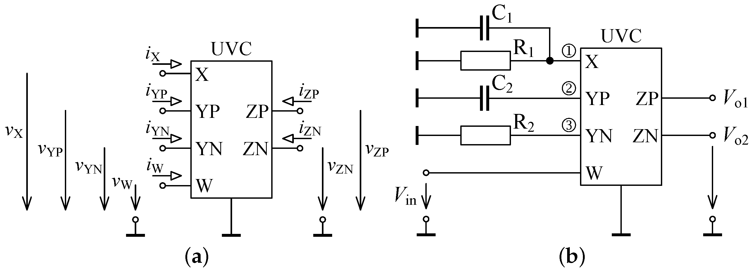
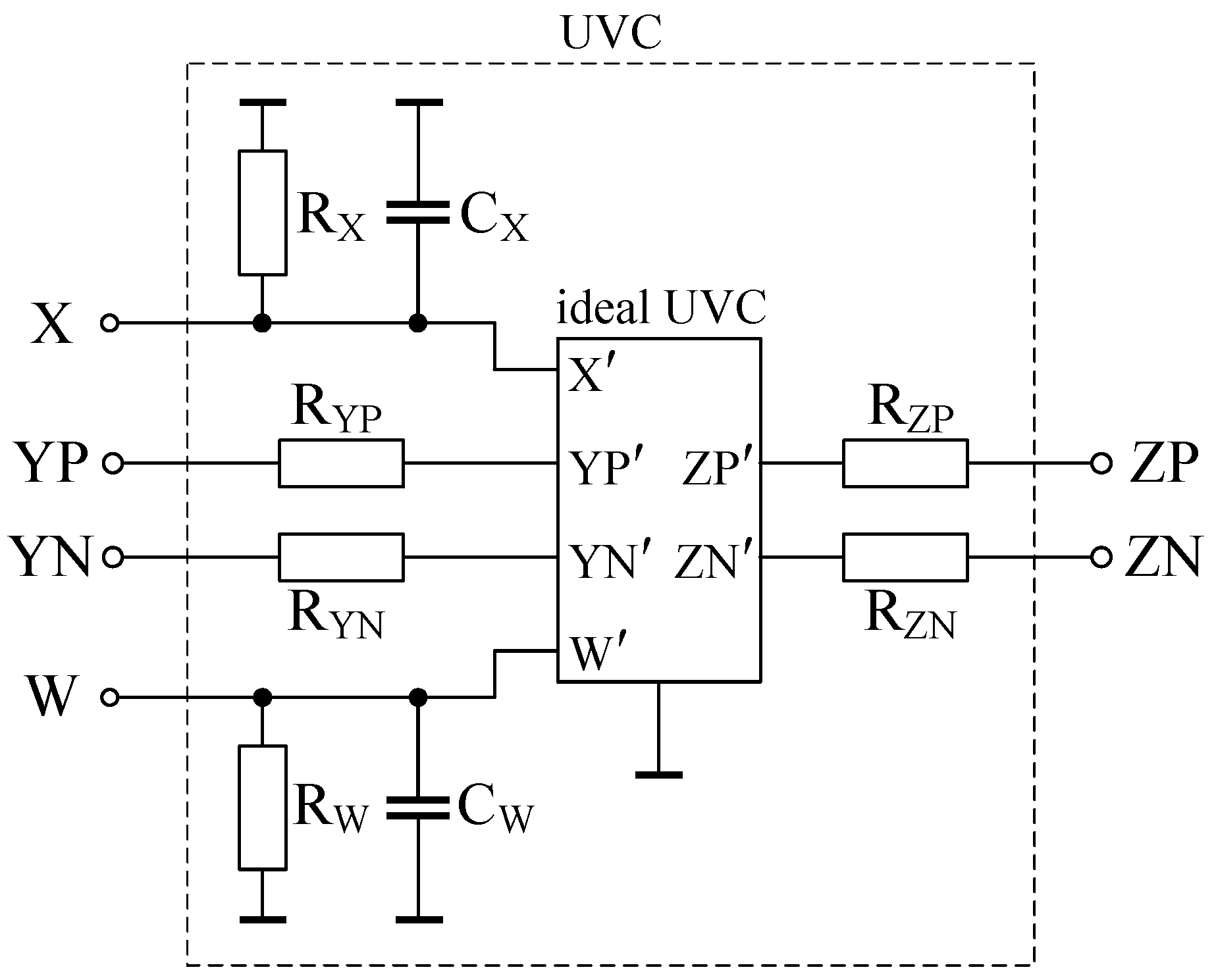
2. Circuit Description

The circuit symbol of the UVC is shown in Figure 1a. Using standard notation, relations between its individual terminals can be described by the following hybrid matrix:
i X v YP v YN i W v ZP v ZN = Y X α 1 ( s ) α 2 ( s ) 0 0 0 0 Z YP 0 δ 1 ( s ) 0 0 0 0 Z YN δ 2 ( s ) 0 0 0 0 0 Y W 0 0 γ 1 ( s ) 0 0 0 Z ZP 0 γ 2 ( s ) 0 0 0 0 Z ZN . v X i YP i YN v W i ZP i ZN ,
where Y X = s C X + 1 / R X , Y W = s C W + 1 / R W are parasitic admittances and Z k = R k ( k = YP, YN, ZP, ZN) are the parasitic resistances at relevant terminals of the UVC, respectively, discussed in detail for the readily available UVC-N1C 0520 chip in [22,23,24]. Parameters α j ( s ) , δ j ( s ) , and γ j ( s ) are, respectively, frequency-dependent non-ideal current and voltage gains for j = { 1 , 2 } . Ideally, these parameters are equal to unity. Using a single-pole model, they can be defined as:
α j ( s ) = α o j 1 + τ α j s , δ j ( s ) = δ o j 1 + τ δ j s , γ j ( s ) = γ o j 1 + τ γ j s .
Here, α o j is DC current, and δ o j and γ o j are DC voltage gains of the UVC, respectively. The bandwidths 1 / τ α j , 1 / τ δ j , and 1 / τ γ j depend on the fabrication of active devices, and in current technologies on the order of a few gigarad/s are ideally equal to infinity. Hence, at low and medium frequencies—i.e., f ( 1 / ( 2 π ) ) × min{ 1 / τ α j , 1 / τ δ j , 1 / τ γ j }—Equation (2) becomes:
α j ( s ) α o j = 1 + ε α i j , δ j ( s ) δ o j = 1 + ε δ v 1 j , γ j ( s ) γ o j = 1 + ε γ v 2 j ,
whereas ε α i j , ε δ v 1 j , and ε γ v 2 j are current and voltage tracking errors, respectively, and satisfy the inequalities | ε α i j | 1 , | ε δ v 1 j | 1 , and | ε γ v 2 j | 1 .
Considering an ideal UVC and assuming R 1 = R 2 = R and C 1 = C 2 = C for the proposed dual-output first-order VM APF shown in Figure 1b, routine analysis yields ideal voltage transfer functions (TFs) in the following forms:
T 1 ( s ) = V o 1 V in = s C R 1 s C R + 1 , T 2 ( s ) = V o 2 V in = s C R 1 s C R + 1 ,
while the phase responses of the TFs (4) are calculated as:
φ 1 ( ω ) = 180 2 arctg ( ω C R ) , φ 2 ( ω ) = 2 arctg ( ω C R ) ,
which indicates that the proposed VM APF can simultaneously provide phase shifting between π (at ω = 0 ) to 0 (at ω = ) and 0 (at ω = 0 ) to π (at ω = ) at output terminals V o 1 and V o 2 , respectively. Finally, both the zero and pole frequencies are equal, and can be found as ω z = ω p = 1 / ( C R ) . Therefore, their sensitivities to passive elements are S C , R ω z , p = 1 ; i.e., are not higher than unity in magnitude.

3. Non-Ideal Analysis

For a complete analysis of the circuit, it is also important consider the main non-idealities of the UVC in Equation (1) as also shown in Figure 2, where:
  • the parasitic resistance R X and parasitic capacitance C X appear between the high-impedance terminal X of the UVC and ground and their values computed in SPICE software are R X = 378.73 k Ω C X = 17.41 pF, respectively,
  • the non-zero parasitic resistance R YP and R YN at two difference current inputs YP and YN have values R YP = 1.27 Ω and R YN = 0.51 Ω, respectively,
  • the parasitic resistance R W and parasitic capacitance C W appear between the auxiliary terminal W of the UVC and ground and their values are R W = 88.19 M Ω C W = 4.19 pF, respectively,
  • the non-zero parasitic resistance R ZP and R ZN at mutually inverse voltage outputs ZP and ZN have values R ZP = 1.01 Ω and R ZN = 0.71 Ω, respectively.
These parameters can be found in greater detail in [22,23,24]. Now, considering the non-idealities listed above, the proposed VM APF suffers from the following non-idealities:
  • at the node ①, a parasitic impedance Z X = 1 / Y X = R X ( 1 / s C X ) can be seen. Note that the capacitance C X and resistance R X can be absorbed into external capacitor C 1 and resistor R 1 , respectively, as they appear in parallel. Hence, in further analysis the total capacitance and resistance at this node will be considered C 1 and R 1 = Z 1 ,
  • the node ② at low-impedance terminal YP is characterized by a parasitic impedance Z YP = R YP , which is in series with external capacitor C 2 , and by assuming it as an impedance Z C 2 = 1 / Y C 2 = 1 / s C 2 , the total impedance at this node can be described as Z C 2 ,
  • finally, the node ③ can be characterized by a parasitic impedance Z YN = R YN , which appears in series with external resistor R 2 = Z 2 . Hence, the total impedance at this node can be labeled as Z 2 .
Considering the non-ideal current and voltage gains of the UVC and simultaneously the effect of the aforementioned non-idealities and re-analyzing the proposed VM APF, the ideal TFs (4) convert to:
T 1 s = γ o 1 Z 1 α o 1 δ o 1 Z 2 α o 2 δ o 2 Z C 2 Z 2 Z C 2 s C 1 Z 1 + 1 , T 2 s = γ o 2 γ o 1 · T 1 s .
Subsequently, the non-ideal zero and pole frequencies differ and can be found as:
ω z = α o 2 δ o 2 α o 1 δ o 1 · Z C 2 Z 2 , ω p = 1 C 1 Z 1 .
The effect of non-idealities on the proposed VM APF can be significantly minimized by the proper selection of external passive components and/or by precise design of the UVC.

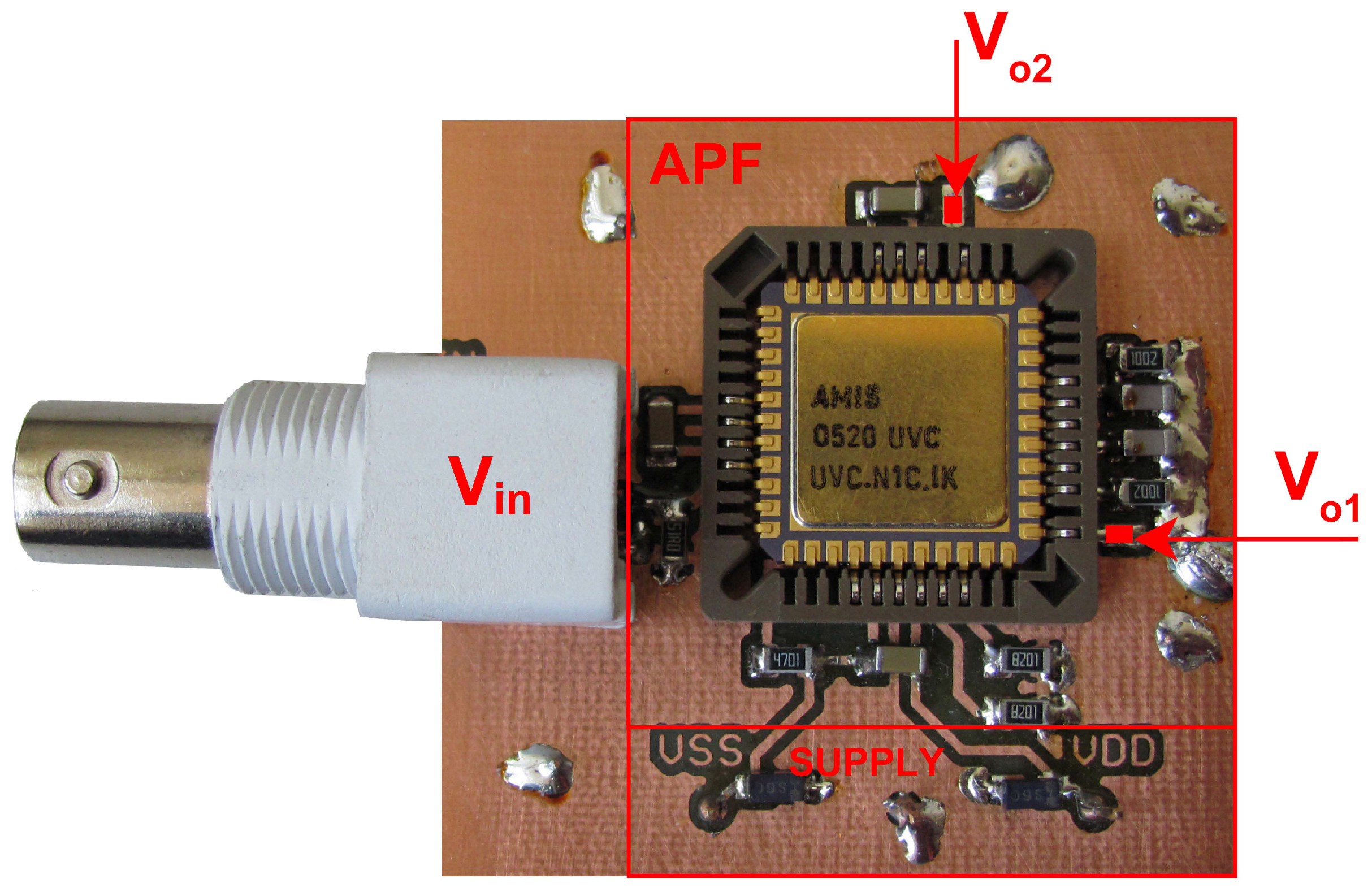
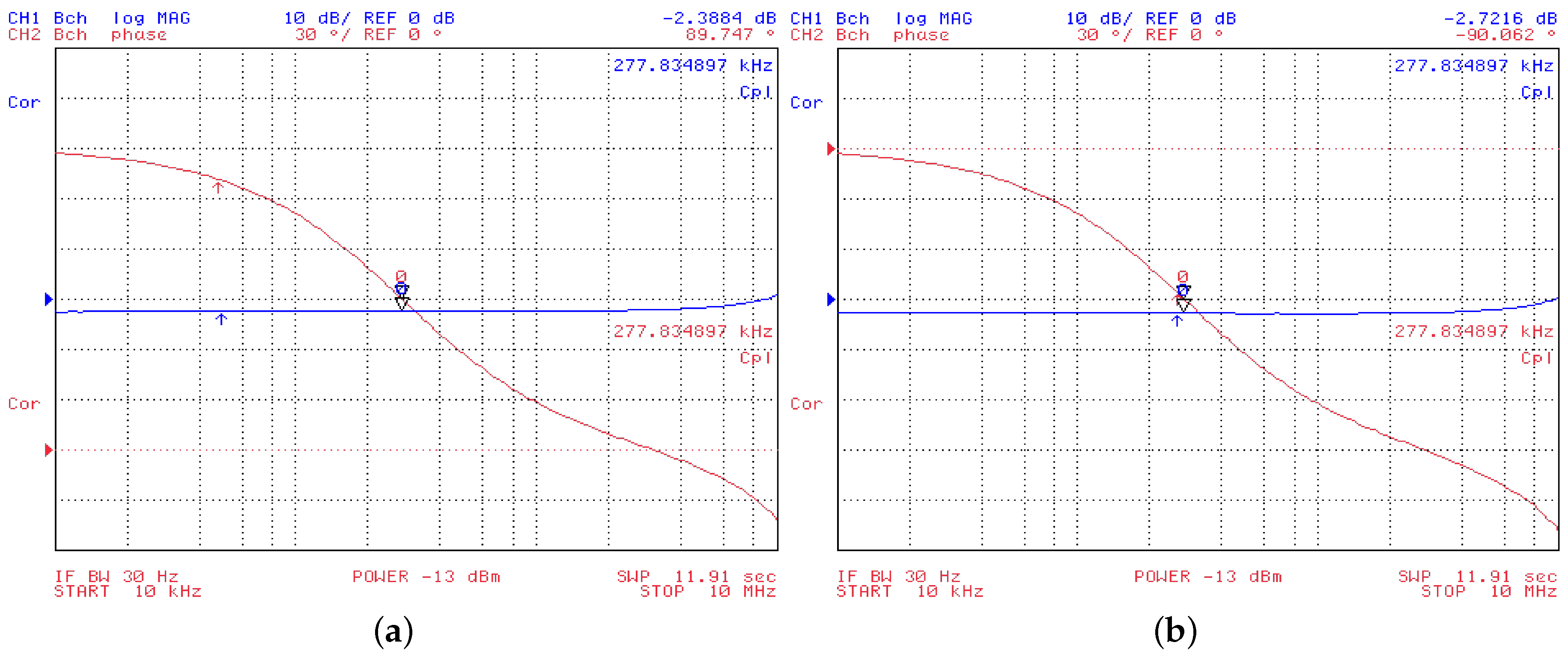
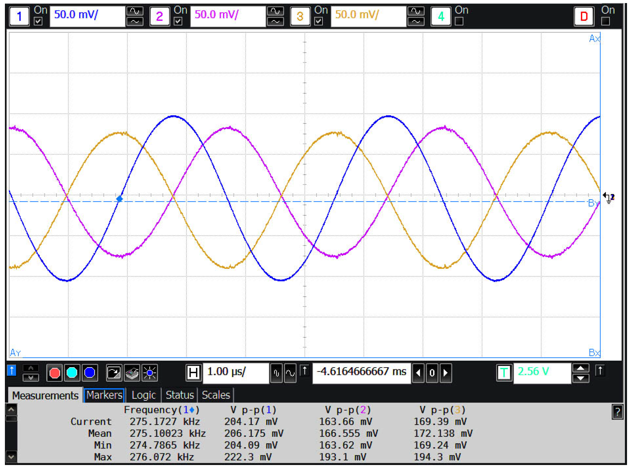
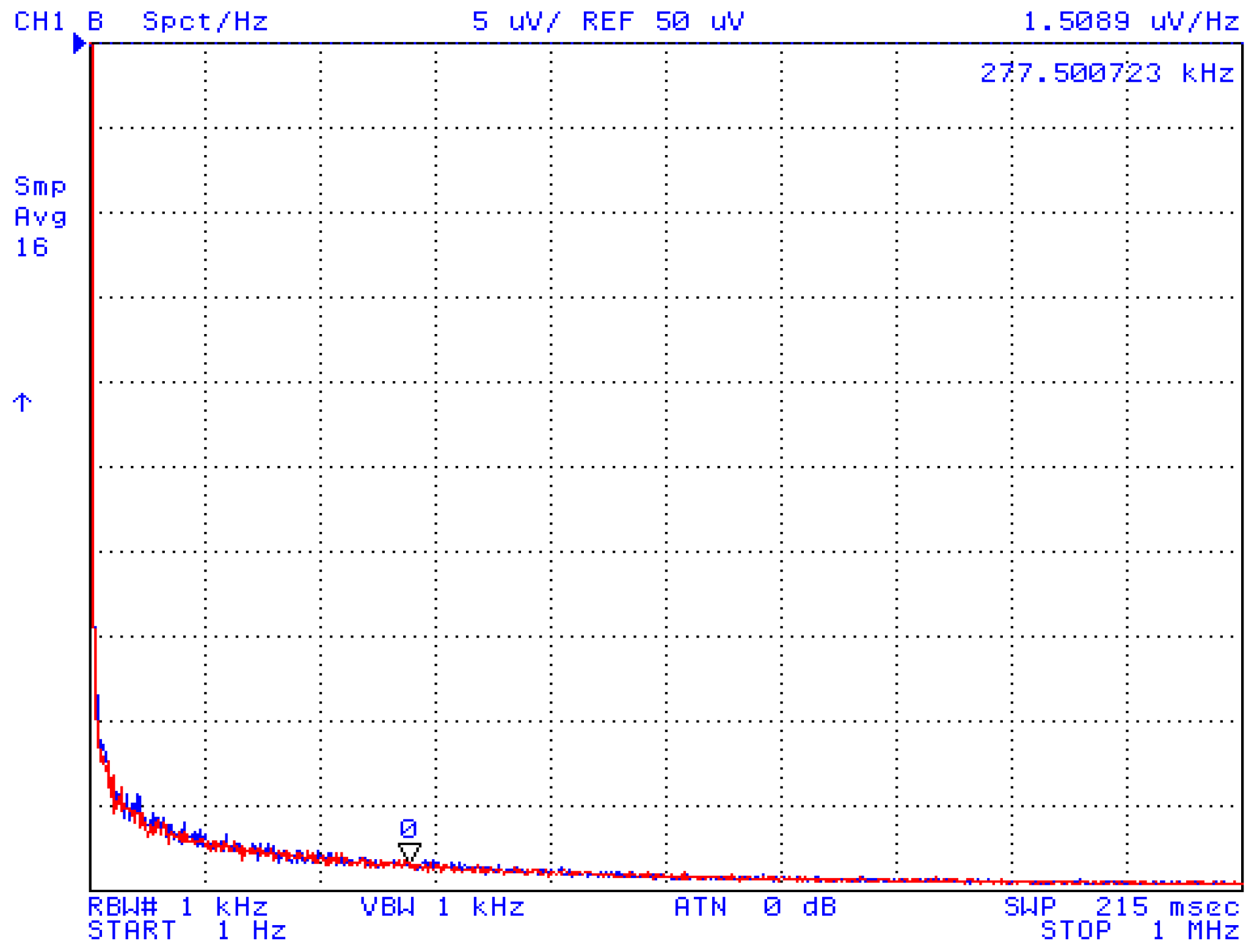
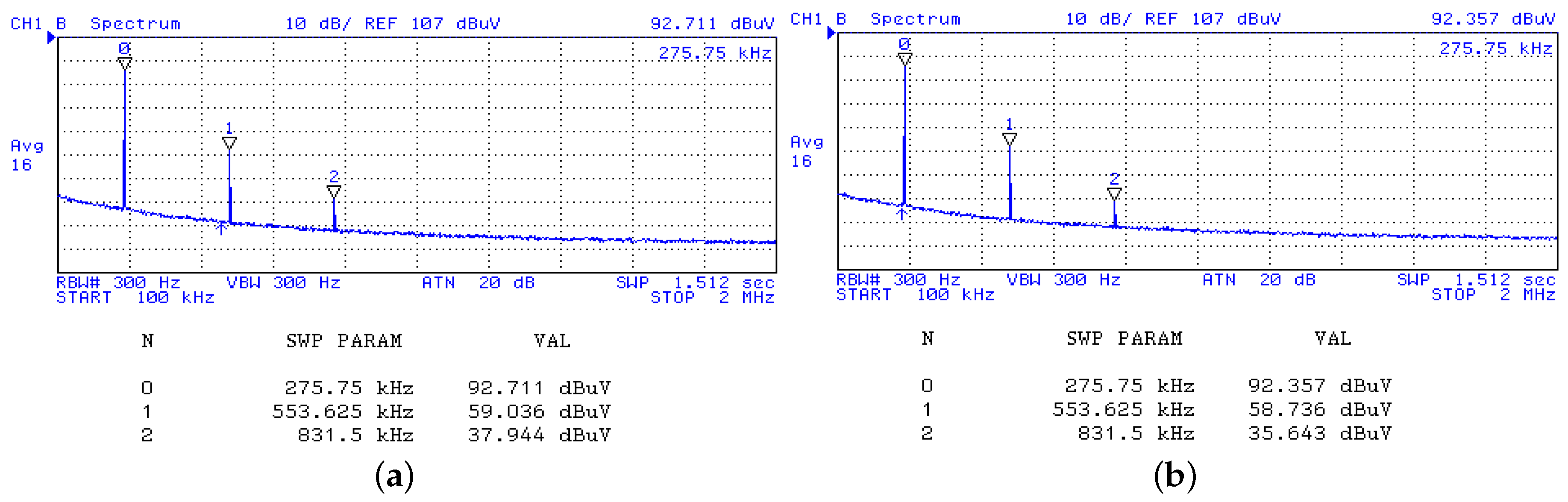
4. Experimental Verification

In order to confirm the theory and prove the real behavior of the proposed VM APF using the readily available UVC-N1C 0520 [22,23,24] chip, a printed circuit board (PCB) was developed, shown in Figure 3. The experimental measurement results were carried out using an Agilent 4395A Network/Spectrum/Impedance Analyzer (Agilent Technologies: Penang, Malaysia). In all measurements, the passive component values of the filter were selected as C 1 = C 2 = 560 pF and R 1 = R 2 = 1 k Ω , which ensures a 90 phase shift at f p _ teor 284.2 kHz. Figure 4a,b illustrate measured gain and phase responses for both inverting and non-inverting outputs, respectively, from which it can be observed that the obtained pole frequency has a value f p _ meas 277.8 kHz and there is an attenuation of about 2.55 dB ± 6 % . Output noise behavior for both responses with respect to frequency are shown in Figure 5. As it can be seen, the noise behavior of both responses are likely the same. For instance, the output noise for V o 2 response at the operating pole frequency was found as 1.5089 μ V / Hz . Measured time-domain responses are depicted in Figure 6, in which a sine-wave input signal of 200 mV pp and frequency of 275 kHz was applied to the filter. Subsequently, the Fourier spectrum of both output signals, showing a high selectivity for the applied signal frequency, is shown in Figure 7a,b, respectively. The total harmonic distortions (THDs) at pole frequency were found as 2.078% and 2.080% for the outputs V o 1 and V o 2 of the proposed filter, respectively. Note that the minor deviations are caused by real behavior of the UVC-N1C 0520 chip and extra parasitic capacitances of the fabricated PCB. The real behavior of the filter is very satisfactory.

5. Conclusions

In this letter, the usefulness and unique features of UVC discussed above have been demonstrated in a VM first-order APF that offers advantages, such as: (i) simultaneously provides both inverting and non-inverting outputs from the same configuration; (ii) easy cascadability due to infinitely high input and zero output-impedances in theory; (iii) use of only grounded passive components (desirable for monolithic integration); (iv) complex passive components matching constraints are not required; (v) simple circuitry employing single ABB. Experimental measurement results based on the readily available UVC-N1C 0520 chip have proven the workability of the proposed VM APF.

Acknowledgments

Research described in this letter was financed by the National Sustainability Program under grant LO1401 and by Czech Science Foundation under grant no. 16-11460Y. For the research, infrastructure of the SIX Center was used.

Author Contributions

Norbert Herencsar conceived the idea and performed the theoretical analysis; Jaroslav Koton and Pavel Hanak performed the experiments and analyzed the results; Norbert Herencsar and Jaroslav Koton wrote the letter.

Conflicts of Interest

The authors declare no conflict of interest.

References

  1. Maheshwari, S. Analogue signal processing applications using a new circuit topology. IET Circ. Device Syst. 2009, 3, 106–115. [Google Scholar] [CrossRef]
  2. Chen, H.P.; Wu, K.H. Grounded-capacitor first-order filter using minimum components. IEICE Trans. Fundam. 2006, E89-A, 3730–3731. [Google Scholar] [CrossRef]
  3. Tran, H.-D.; Wang, H.-Y.; Lin, M.-C.; Nguyen, Q.-M. Synthesis of cascadable DDCC-based universal filter using NAM. Appl. Sci. 2015, 5, 320–343. [Google Scholar] [CrossRef]
  4. Kartci, A.; Sotner, R.; Jerabek, J.; Herencsar, N.; Petrzela, J. Phase shift keying modulator design employing electronically controllable all-pass sections. Analog Integr. Circ. Signal Process. 2016, 89, 781–800. [Google Scholar] [CrossRef]
  5. Biolek, D.; Biolkova, V. All-Pass Filters Employing Differential Op-Amps. Electron. World 2010, 116, 44–45. [Google Scholar]
  6. Biolkova, V.; Kolka, Z.; Biolek, D. Dual-output all-pass filter employing fully-differential operational amplifier and current-controlled current conveyor. In Proceedings of the 2011 7th International Conference on Electrical and Electronics Engineering (ELECO), Bursa, Turkey, 1–4 December 2011; pp. 340–344.
  7. Chen, H.-P.; Lin, M.-T.; Yang, W.-S. Novel first-order non-inverting and inverting output of all-pass filter at the same configuration using ICCII. IEICE Trans. Electron. 2006, 89-C, 865–867. [Google Scholar] [CrossRef]
  8. Mohan, J.; Maheshwari, S.; Chauhan, D.S. Minimum component based first-order inverting and non-inverting outputs of all-pass filter at the same circuit. ACEEE Int. J. Electr. Power Eng. 2010, 1, 32–35. [Google Scholar]
  9. Chaturvedi, B.; Mohan, J. Single DV-DXCCII based voltage controlled first order all-pass filter with inverting and non-inverting responses. Iran. J. Electr. Electron. Eng. 2015, 11, 301–309. [Google Scholar]
  10. Herencsar, N.; Minaei, S.; Koton, J.; Yuce, E.; Vrba, K. New resistorless and electronically tunable realization of dual-output VM all-pass filter using VDIBA. Analog Integr. Circ. Signal Process. 2013, 74, 141–154. [Google Scholar] [CrossRef]
  11. Herencsar, N.; Koton, J.; Vrba, K. A new electronically tunable voltage-mode active-C phase shifter using UVC and OTA. IEICE Electron. Express 2009, 6, 1212–1218. [Google Scholar] [CrossRef]
  12. Herencsar, N.; Koton, J.; Vrba, K.; Cicekoglu, O. High-input and low-output impedance voltage-mode all-pass filter using single universal voltage conveyor. In Proceedings of the International Conference on Telecommunications and Signal Processing TSP 2010, Baden near Vienna, Austria, 17–20 August 2010; pp. 42–46.
  13. Herencsar, N.; Koton, J.; Jerabek, J.; Vrba, K.; Cicekoglu, O. Voltage-mode all-pass filters using universal voltage conveyor and MOSFET-based electronic resistors. Radioengineering 2011, 20, 10–18. [Google Scholar]
  14. Metin, B.; Herencsar, N.; Koton, J. Cascadable all-pass filter using a single universal voltage conveyor. In Proceedings of the 2012 22nd International Conference Radioelektronika (RADIOELEKTRONIKA), Brno, Czech Republic, 17–18 April 2012; pp. 97–100.
  15. Filanovsky, I.M.; Stromsmoe, K.A. Current-voltage conveyor. Electron. Lett. 1981, 17, 129–130. [Google Scholar] [CrossRef]
  16. Salama, K.; Soliman, A. Novel MOS-C quadrature oscillator using the differential current voltage conveyor. In Proceedings of the 42nd Midwest Symposium on Circuits and Systems, Las Cruces, NM, USA, 8–11 August 1999; pp. 279–282.
  17. Acar, C.; Ozoguz, S. A new versatile building block: Current differencing buffered amplifier suitable for analog signal processing filters. Microelectron. J. 1999, 30, 157–160. [Google Scholar] [CrossRef]
  18. Pathak, J.K.; Singh, A.K.; Senani, R. New canonic lossy inductor using a single CDBA and its application. Int. J. Electron. 2016, 103, 1–13. [Google Scholar] [CrossRef]
  19. Minarcik, M.; Vrba, K. Single-input six-output voltage-mode filter using universal voltage conveyors. IEICE Trans. Fundam. 2008, E91-A, 2035–2037. [Google Scholar] [CrossRef]
  20. Koton, J.; Vrba, K.; Herencsar, N. Tuneable filter using voltage conveyors and current active elements. Int. J. Electron. 2009, 96, 787–794. [Google Scholar] [CrossRef]
  21. Koton, J.; Herencsar, N.; Vrba, K. Minimal configuration precision full-wave rectifier using current and voltage conveyors. IEICE Electron. Express 2010, 7, 844–849. [Google Scholar] [CrossRef]
  22. Koton, J.; Herencsar, N.; Vrba, K. KHN-equivalent voltage-mode filters using universal voltage conveyors. AEU Int. J. Electron. Commun. 2011, 65, 154–160. [Google Scholar] [CrossRef]
  23. Sponar, R.; Vrba, K. Measurements and behavioral modelling of modern conveyors. Int. J. Comput. Sci. Netw. Secur. 2006, 6, 57–65. [Google Scholar]
  24. UVC-N1C 0520 Datasheet; Universal Voltage Conveyor: ON Semiconductor & Brno University of Technology, Czech Republic. 2010. Available online: www.utko.feec.vutbr.cz/∼herencsar/UVC_N1C_0520.pdf (accessed on 10 February 2017).
Figure 1. (a) Circuit symbol of UVC; (b) proposed new voltage-mode first-order all-pass filter.
Applsci 07 00307 g001
Figure 2. Main parasitic resistance and capacitance of the UVC.
Applsci 07 00307 g002
Figure 3. Developed printed circuit board (PCB) prototype.
Applsci 07 00307 g003
Figure 4. Measured magnitude (blue line) and phase (red line) responses of the VM APF for outputs: (a) V o 1 ; (b) V o 2 with cursor position at f p _ meas .
Applsci 07 00307 g004
Figure 5. Measured noise variations for both voltage outputs versus frequency (red line— V o 1 , blue line— V o 2 ).
Applsci 07 00307 g005
Figure 6. Measured time-domain waveforms (blue line—input, orange line— V o 1 , pink line— V o 2 ).
Applsci 07 00307 g006
Figure 7. Measured Fourier spectrum of the output signals: (a) V o 1 , (b) V o 2 .
Applsci 07 00307 g007
Table 1. Comparative study of existing dual-output voltage-mode (VM) all-pass filters (APFs).
ReferenceABB TypeGrounded R/CFloating R/CSimul./Meas. f p (Hz)Supply (V)
Figure 4b in [5]FD-OPA & CCII0/01/1Meas.29.6 k±5
Figure 1 in [6]FD-OPA0/00/1Simul.92 k±1.5
Figure 2 in [7]ICCII+0/01/1Simul.1.59 M±1.25
Figure 2 in [8]FDCCII0/11/0Simul.159.2 k±3
Figure 2 in [9]DV-DXCCII & 1 NMOS0/10/0Simul.27 M±0.9
Figure 3 in [10]VDIBA0/00/1BothS: 9.44 M; M: 1 M±0.9; ±5
Figure 1 in [11]UVC & OTA0/00/1Simul.3 M±2
Figure 3 in [12]UVC2/01.IBothS: 3.5 M; M: 160.4 k±2.5; ±1.65
Figure 2a in [13]UVC2/00/1Simul.1.17 M±2.5
Figure 2b in [13]UVC2/00/1BothS: 1.17 M; M: 746.4 k±2.5; ±1.65
Figure 2 in [14]UVC0/12/0Simul.390 k±2.5
This workUVC2/20/0Meas.277.8 k±1.65
Note: S.: simulation result; M.: measurement result. CCII: second-generation current conveyor; DV-DXCCII: differential voltage dual-X second-generation current conveyor; FD-OPA: fully-differential operational amplifier; FDCCII: fully differential second-generation current conveyor; ICCII+: positive-type inverting second-generation current conveyor; OTA: operational transconductance amplifier; UVC: universal voltage conveyor; VDIBA: voltage differencing inverting buffered amplifier; NMOS: n-type metal-oxide-semiconductor.

