Article

Theoretical Exposure Dose Modeling and Phase Modulation to Pattern a VLS Plane Grating with Variable-Period Scanning Beam Interference Lithography

1
College of Instrumentation and Electrical Engineering, Jilin University, Changchun 130012, China
2
Changchun Institute of Optics, Fine Mechanics and Physics, Chinese Academy of Sciences, Changchun 130033, China
*
Author to whom correspondence should be addressed.
Appl. Sci. 2022, 12(15), 7946; https://doi.org/10.3390/app12157946
Submission received: 3 June 2022 / Revised: 28 July 2022 / Accepted: 5 August 2022 / Published: 8 August 2022

Abstract

:
Variable-period scanning beam interference lithography (VP-SBIL) can be used to fabricate varied-line-spacing (VLS) plane gratings. The exposure phase modulation method to pattern a VLS grating with a desired groove density must be carefully devised. In this paper, a mathematical model of the total exposure dose for VLS plane grating fabrication is established. With model-based numerical calculations, the phase modulation effects of the parameters, including the fringe locked phase, fringe density, and step size, are analyzed. The parameter combinations for the phase modulation are compared and chosen, and the optimal coordinate for phase compensation is selected. The calculation results show that the theoretical errors of the groove density coefficients can be controlled within 1e-8. The mathematical model can represent the deposited exposure dose for patterning VLS gratings during the lithography process, and the chosen parameters and proposed phase modulation method are appropriate for patterning VLS gratings with VP-SBIL.

1. Introduction

A varied-line-spacing (VLS) plane grating is a straight groove periodic structure with a desired groove density function. VLS plane grating can self-focus and reduce aberration. The efficiency and resolving power of instruments can be improved. Compared with the concave grating, the substrate is easy to process. VLS plane gratings are widely used as key components in extreme ultraviolet spectrum analysis, monochromators, spectral imaging, and position sensors [1,2,3,4,5,6].
The most popular methods to pattern VLS plane gratings are diamond ruling, holographic imaging, and electron or laser beam lithography. Traditional direct-write methods such as diamond ruling and electron-beam or laser beam lithography can be extremely slow and expensive, and result in gratings with undesired phase errors [1,2,7]. Holographic gratings written by two-beam interference introduced a cost-effective path to more rapidly produce gratings with smoother phases. However, holographic methods require spherical or aspheric wavefront recording optics. The desired groove density frequently has difficulty satisfying geometrical constraints in spherical wavefront recording systems, and groove bending decreases the spectral resolution of the grating. Aspheric wavefront recording optics are complicated to design, manufacture, and align. The deviation and error from the recording optics introduce errors into the groove density distribution [8,9].
A variable-period scanning beam interference lithography (VP-SBIL) system is an effective tool to pattern high-fidelity general periodic structures in one or two dimensions within a short period. The VP-SBIL system uses small Gaussian beams with diameters of several micrometers to millimeters to form fringes in a small interference image. The image has a very high phase fidelity. The fringe period and orientation can be progressively changed in a desirable fashion. The fringe phase can be locked using a high-bandwidth fringe locking system. The grating substrate is scanned under the image using a high-performance stage. A uniform exposure dose is achieved by overlapping the subsequent scans. The patterning process is fast and cost-effective because the interference image contains several hundred or thousands of fringes, and expensive aspheric optics are not required in VP-SBIL [10,11,12].
Fabricating a VLS grating with VP-SBIL is not as straightforward as the direct-write method. The groove density of the grating represents the grating phase distribution, which is determined by the exposure phase modulation. To fabricate a straight groove VLS grating using VP-SBIL, three questions must be answered. First, how to express the total exposure dose for patterning a VLS grating with VP-SBIL? Second, which parameters are chosen for the exposure phase modulation? Third, how to cooperatively regulate these parameters to acquire the desired phase distribution? In the published articles about VP-SBIL, the optical topology and basic manufacturing principle for variable-period structures are illustrated. However, details about the phase modulation are not mentioned [10,11,12]. We attempt to provide possible and simple answers to these questions. This is a key issue for practical applications of VP-SBIL [13,14,15].
This paper establishes a model of the total exposure dose for a VLS plane grating patterned with VP-SBIL. The exposure phase distribution and exposure contrast in an intuitive manner are verified, and the phase modulation effects of the parameters are given. The parameter selection for the phase modulation and the optimal coordinate for phase compensation to pattern the VLS grating are proposed. The results for an actual VLS plane grating are given. Finally, the reasons for the differences in the phase modulation performance and phase compensation are discussed.

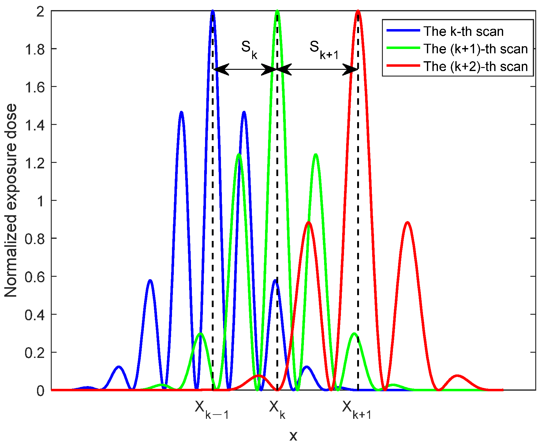
2. Model of the Total Exposure Dose for VLS Grating Patterning

The desired groove density function of the VLS plane grating without higher-order aberration compensation can be expressed as follows
g ( x ) = n g 0 + n g 1 ( x W g / 2 )
The desired phase variation of the VLS grating can be expressed as
Φ g ( x ) = 2 π 0 x g ( x ) d x = 2 π [ ( n g 1 / 2 ) x 2 + ( n g 0 n g 1 W g / 2 ) x ]
where the x coordinate is along the vector direction of the grating. It is assumed that x = 0 is at the margin of the grating substrate. Wg is the grating width along the x-axis; ng0 is the groove density in the center of the grating with units of L/mm; ng1 is the slope with units of L/mm2; and ng0 and ng1 are determined according to the aberration correction principle of the VLS grating and the structure of the spectrometer or the device, respectively.
In the VP-SBIL system, the step direction is along the x-axis, and the scanning direction is along the y-axis, which is parallel to the fringe direction. In this paper, the VLS grating was patterned with substrate parallel scanning. At the end of a scan, the stage stepped over and reversed direction for a new scan. The exposure phase was modulated during the step process, and the phase relative to the substrate remained unchanged during scanning. Other written modes such as Doppler scanning are not described here [16,17].
Let us assume a perfect stage scan, fringe period regulation, and fringe phase locking. The initial scan is at x = X0 = 0. The fringe density in the initial scan is f0. The dose delivered to the resist can be mathematically written as
D 0 ( x ) = B ( x ) + A ( x ) cos ( 2 π x f 0 + δ 0 )
where B(x) is the background dose. δ0 is the locked phase introduced by the fringe locking unit in the initial scan. A(x) is the normalized Gaussian dose amplitude in the x-direction and is expressed as
A ( x ) = exp ( 2 x 2 / ω 2 )
where ω is the 1/e2 radius of the Gaussian intensity envelope [16,17].
A uniform exposure dose is achieved by overlapping subsequent scans. After the first step with a step size S1, x = X1 = S1 and its serial number k = 1. The dose deposited by the second scan (k = 1) is expressed as
D 1 ( x ) = B ( x X 1 ) + A ( x X 1 ) cos [ 2 π f 1 ( x X 1 ) + δ 1 ]
where f1 is the fringe density in the second scan, and δ1 is the phase introduced by the fringe locking unit.
Similarly, the exposure dose deposited by the (k + 1)-th scan after k steps (k ≥ 1) is equal to the initial dose, but it has shifted in position due to the discrete stepping of the stage, which can be expressed with Equation (6). This is illustrated in Figure 1 (the fringe density is exaggerated for clarity).
D k ( x ) = B ( x X k ) + A ( x X k ) cos [ 2 π f k ( x X k ) + δ k ]
where Sk is the k-th step size. The (k + 1)-th scan is at x = Xk = i = 1 k S i after k steps. fk and δk are the fringe density and locked phase introduced by the fringe locking unit in the (k + 1)-th scan, respectively.
fk (k ≥ 1) can be written as f k = f k 1 + Δ k = f 0 + i = 1 k Δ i , where Δk is the density increment between the (k + 1)-th scan and the k-th scan. Equation (6) can be rewritten as
D k ( x ) = B ( x X k ) + A ( x X k ) cos ( 2 π f 0 x + φ k )
where φk is the phase increment between the (k + 1)-th scan and the initial scan, which can be expressed as
φ k ( x ) = 2 π ( x i = 1 k Δ i     f 0 X k X k i = 1 k Δ i ) + δ k
From Equation (8), the phase increment between the (k + 1)-th scan and k-th scan can be expressed as
φ k d ( x ) = φ k ( x ) φ k 1 ( x ) = φ k d x ( x ) + φ k d c + ( δ k δ k 1 )
where φkdx(x) is the term varying with x, φkdx(x) = 2πxΔk. φkdc is the term independent of x. φkdc = −2π (Xk−1Δk + Skfk).
The resist on the substrate is deposited after N steps and N + 1 scans. The total exposure dose in the resist is the sum of all individual doses and can be expressed as
D T ( x ) = D 0 ( x ) + D 1 ( x ) + D N ( x ) = D T B ( x ) + A T ( x ) cos Ψ T ( x )
where DTB(x) is the total background dose, AT(x) is the total dose amplitude, and ΨT(x) is the exposure phase distribution. They can be expressed with Equations (11) and (12).
D T B ( x ) = B ( x ) + B ( x X 1 ) + B ( x X k )
A T ( x ) cos Ψ T ( x ) = A ( x ) cos ( 2 π f 0 x + φ 0 ) + A ( x X 1 ) cos ( 2 π f 0 x + φ 1 ) + A ( x X N ) cos ( 2 π f 0 x + φ N )
From Equation (12), AT(x) and ΨT(x) can be expressed as
{ A T ( x ) = E ( x ) 2 + F ( x ) 2 Ψ T ( x ) = 2 π x f 0 + Ψ ( x ) Ψ ( x ) = arctan [ F ( x ) / E ( x ) ] E ( x ) = A ( x ) cos φ 0 + A ( x X 1 ) cos φ 1 + A ( x X N ) cos φ N F ( x ) = A ( x ) sin φ 0 + A ( x X 1 ) sin φ 1 + A ( x X N ) sin φ N
Let us assume that the resist on the substrate is uniform and linear to the exposure dose. ΨT(x) determines the theoretical phase distribution of the fabricated grating. The phase error between the fabricated grating and the desired grating can be expressed as
Φ e ( x ) = Ψ T ( x ) Φ g ( x )
The patterned grating with the desired g(x) can be acquired under the condition of Φe(x) = 0, which is the goal of the phase modulation. The total exposure contrast can be expressed as
γ ( x ) = A T ( x ) / D T B ( x )
Equations (10)–(13) are the mathematical exposure dose model for the VLS grating exposure with VP-SBIL in the parallel scanning style. If fk is constant in all scans, the dose model coincides with that in equal-period SBIL (EP-SBIL) [18,19].

3. Phase Modulation Effects of the Parameters and Parameter Selection

3.1. General Parameters and Numerical Calculation

As shown in Equations (8) and (13), ΨT(x) is mainly determined by the locked phase δk, fringe density fk, and step size Sk from all of the scans. Fortunately, all of these parameters can be adjusted in a VP-SBIL system. However, ΨT(x) cannot be expressed with a simple mathematical form. It is difficult to directly solve the equation Φe(x) = 0. The numerical calculation based on the exposure model is an effective means of analysis.
For simplicity, assume that the contrast in a single scan is 1, which implies that A (x) = B (x) in Equation (3). A grating in a surface physics beamline monochromator is taken as an example. The parameters of the grating are Wg = 30 mm, ng0 = 1200 L/mm, and ng1 = −0.7783 L/mm2 [20]. To avoid fringe smearing in VP-SBIL, a spot diameter in the range of 10–100 microns is optimal [11]. We chose ω = 100 μm for the numerical calculation and analysis. To achieve a uniform exposure dose, the adjacent scans overlap. As described in previous research on EP-SBIL, the step size is smaller, the uniformity and contrast decrease caused by phase error are better, but the exposure is slower. If the fringe period is constant in all scans, a step size of 0.9 times the 1/e2 radius (StepRatio = Sk/ω = 0.9) produces a better dose uniformity than 1% [18,19]. VLS grating fabrication requires fringe phase modulation in each step process, which implies that phase inconsistency in the adjacent scans is inevitable. The step size should decrease with increasing the coefficient ng1 to satisfy the exposure contrast demand. As StepRatio is not a crucial parameter for phase modulation, we arbitrarily chose StepRatio = 0.8 for the small ng1 value in this paper.
With the above general parameters, the numerical calculation was developed with Matlab. To minimize the numerical artifact that may arise from an abrupt data cutoff, the total step-scan width Wt is larger than Wg (Wt = Wg + 1 mm), and a sufficiently wide x range [−5 mm, Wt + 5 mm] is chosen for calculation. To guarantee calculation precision, the calculation step is taken to be 1/100 times ω. Based on the exposure model, the exposure doses are calculated and accumulated step by step in the same way as those in a real exposure process, and Фe(x) and γ(x) are calculated according to Equations (14) and (15). Because of the lack of sufficient overlap at the start and end scan segments, the data from x = 0 to x = Wg are the focus. To observe the effect of δk, fk, and Sk on ΨT(x), three phase modulation manners by varying these parameters in an intuitive way with other parameters remaining unchanged are demonstrated. These approaches appeared to be feasible and needed to be verified, and the modulation effects of the parameters were analyzed. According to the numerical calculation results, the parameters for phase modulation were chosen.

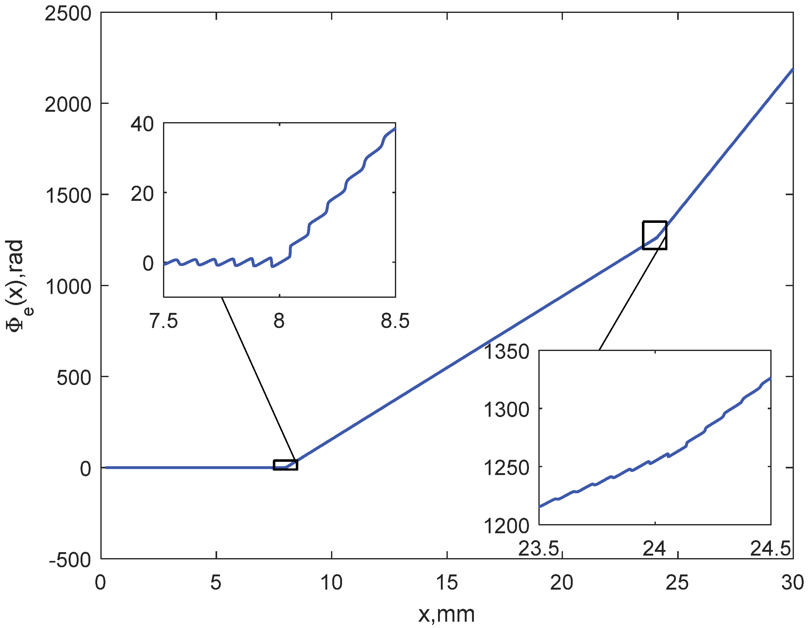
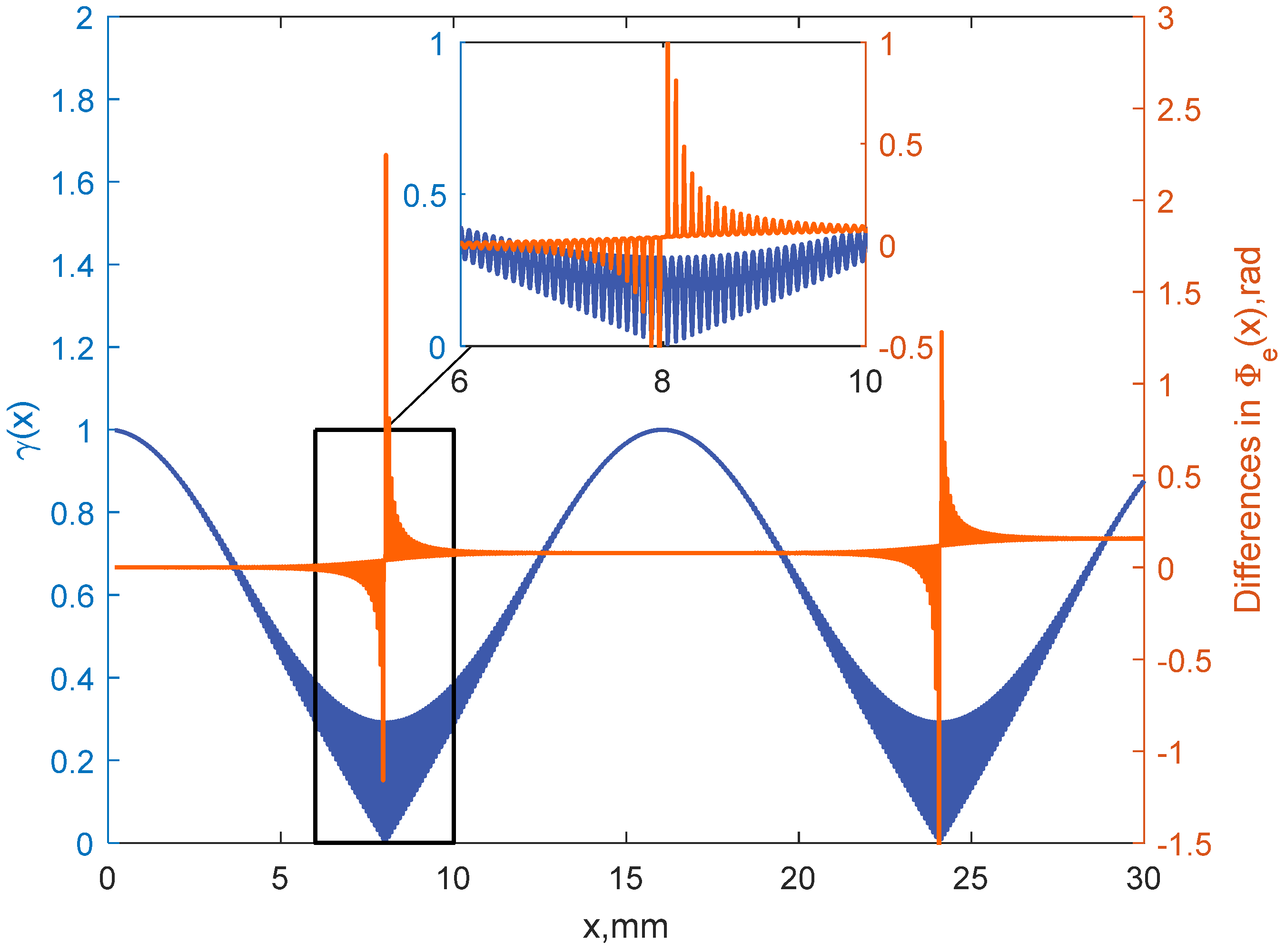
3.2. Phase Modulation Effects of the Parameters

3.2.1. Phase Modulation by Varying Only δk

Set the fringe density to a constant value of fk = f0 = ng0ng1 Wg/2. It is equal to the desired density at x = 0. The step size is an integral multiple of the fringe period as that in a traditional EP-SBIL, which implies that Sk = Nsteps/f0 and Xk = kNsteps/f0. Nsteps influences the dose uniformity and exposure contrast. For general VLS gratings with a small coefficient ng1, the grating density is mainly determined by ng0. Therefore, Nsteps is chosen as a constant expressed as
N s t e p s = r o u n d ( ω S t e p R a t i o n g 0 )
Under these conditions, Equation (8) changes to a simple form φk(x) = δk. If δk is used for phase modulation, all fringes in the image have identical phase variations, which implies that δk cannot be expressed as a function of the x coordinate.
  • Intuitively varying δk according to Фg(x)
Intuitively, changing the δk value with the desired Фg phase in the (k + 1)-th scan appears to be feasible, which can be written as
δ k = Φ g ( X k ) = 2 π [ ( n g 1 / 2 ) X k 2 + ( n g 0 n g 1 W g / 2 ) X k ]
Фe(x) is shown in Figure 2, and it is basically piecewise linear with a transition region between the two adjacent linear segments. The exposure contrast is shown in Figure 3. The troughs of the exposure are in contrast with an amplitude close to zero. We performed a differential operation to Фe(x). The differences in Фe(x) are also shown in Figure 3. The x coordinates of the cusps in Фe(x) coincide with those of the lowest contrasts. The frequency components of the exposure contrast are extracted using FFT (Fast Fourier Transform). Two main frequency components are approximately located at Fp1 = |0.5ng1|/(2π) and Fp2 = 1/Sk. The Fp1 component is influenced by the linear variation of the grating density. The Fp2 component is caused by the phase inconsistency in adjacent scans, which also exists in Фe(x), as shown in Figure 3. Фe(x) and γ(x) cannot satisfy the demands of grating fabrication.
2.
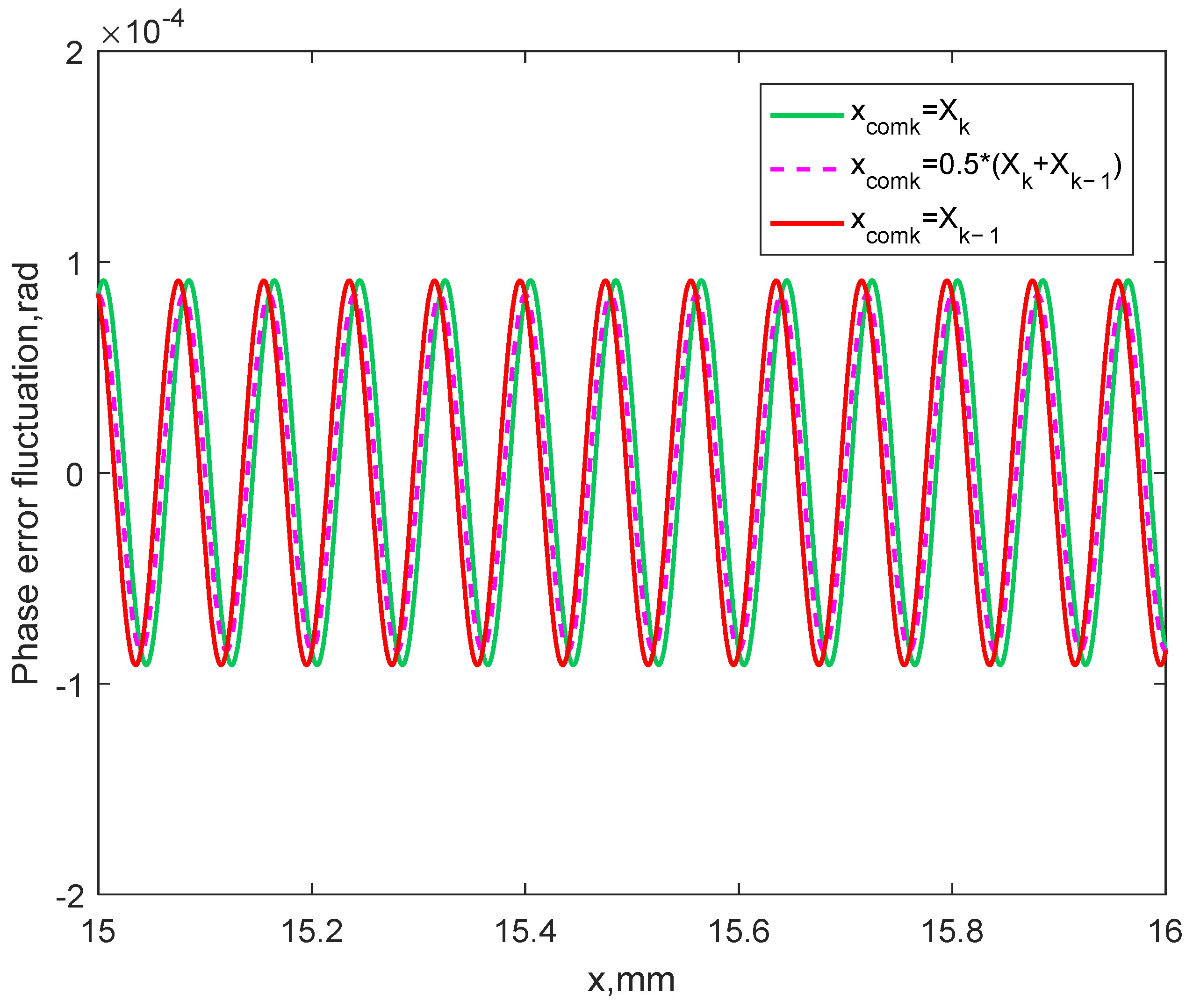
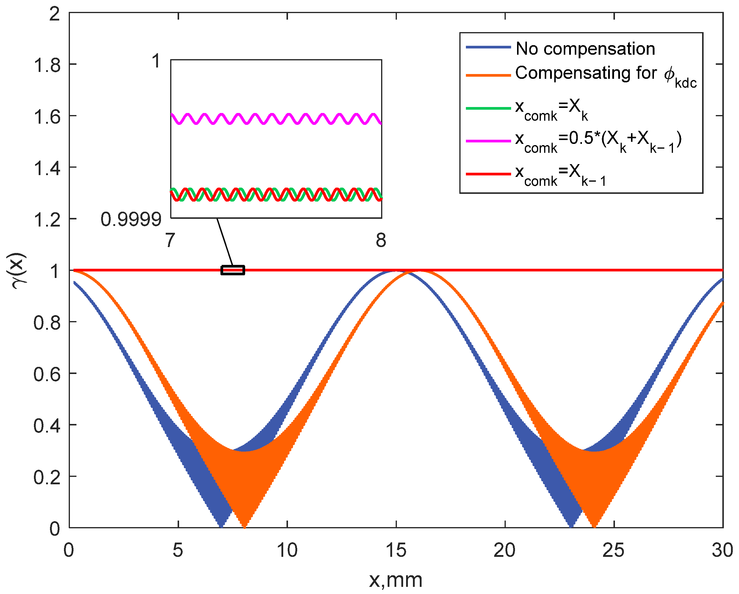
Phase modulation effect by only varying δk according to Xk
To modulate the phase by only varying δk, δk is different at different Xk. As shown in Equation (2), the desired phase variation is a quadratic polynomial. More generally, δk can be written in an analogous form expressed as
δ k = 2 π ( a δ 2 X k 2 + a δ 1 X k + a δ 0 )
Through numerical calculation and theoretical analysis, the modulation effects of δk are as follows.
(1) aδ2 = aδ1 = 0, and φk = δc = 2πaδ0. The phase increments are constant for all scans. From Equation (13), ΨT(x) can be expressed as
Ψ T ( x ) = 2 π f 0 x + δ c
The patterned grating is an equal-period grating with density f0. The constant phase shift introduced by δc does not affect the grating characteristics. From Equation (15), γ(x) = 1.
(2) aδ2 = 0, φk = δk = 2π (aδ1Xk + aδ0). ΨT(x) is a linear function with the Fp2 frequency component. The slope is influenced by aδ1, and the constant term and γ(x) are determined by aδ1 and aδ0. If the absolute value of aδ1 is small, the slope of ΨT(x) is approximately 2π (f0 + aδ1), which implies that aδ1 can be used to change the period of the patterned grating. This conclusion is consistent with the phenomenon found in an EP-SBIL in Ref. [21]. γ(x) is an average exposure contrast plus an Fp2 frequency component. With a constant step size and small aδ1, aδ1 is smaller, the average exposure contrast is higher, and the amplitude of the Fp2 component is smaller. With the general parameters for numerical calculation, the average γ(x) is better than 0.9 when |aδ1| < 1.4. To maintain the exposure contrast, the adjustment range of the grating density is limited to ±1.4 L/mm.
(3) aδ2 ≠ 0, aδ1 ≠ 0 and aδ0 ≠ 0. ΨT(x) and Фe(x) are basically piecewise quadratic polynomials. δk expressed with Equation (17) is a special case of this situation. Фe(x) in Figure 2 is the piecewise quadratic with a quadratic coefficient of zero. The results are similar to those in Figure 2 and Figure 3. Фe(x) increases with x, and γ(x) fluctuates between 0 and 1. The cusps of Фe(x) and the lowest γ(x) are located at the same x coordinates, and their spatial frequency is |aδ2|/(2π). There is also the Fp2 frequency component caused by the phase inconsistency in the adjacent scans.
In other words, the desired VLS grating cannot be obtained by only varying δk in the form in Equation (18). δk can compensate for a certain phase error or change the density of an equal-period grating in a small range.

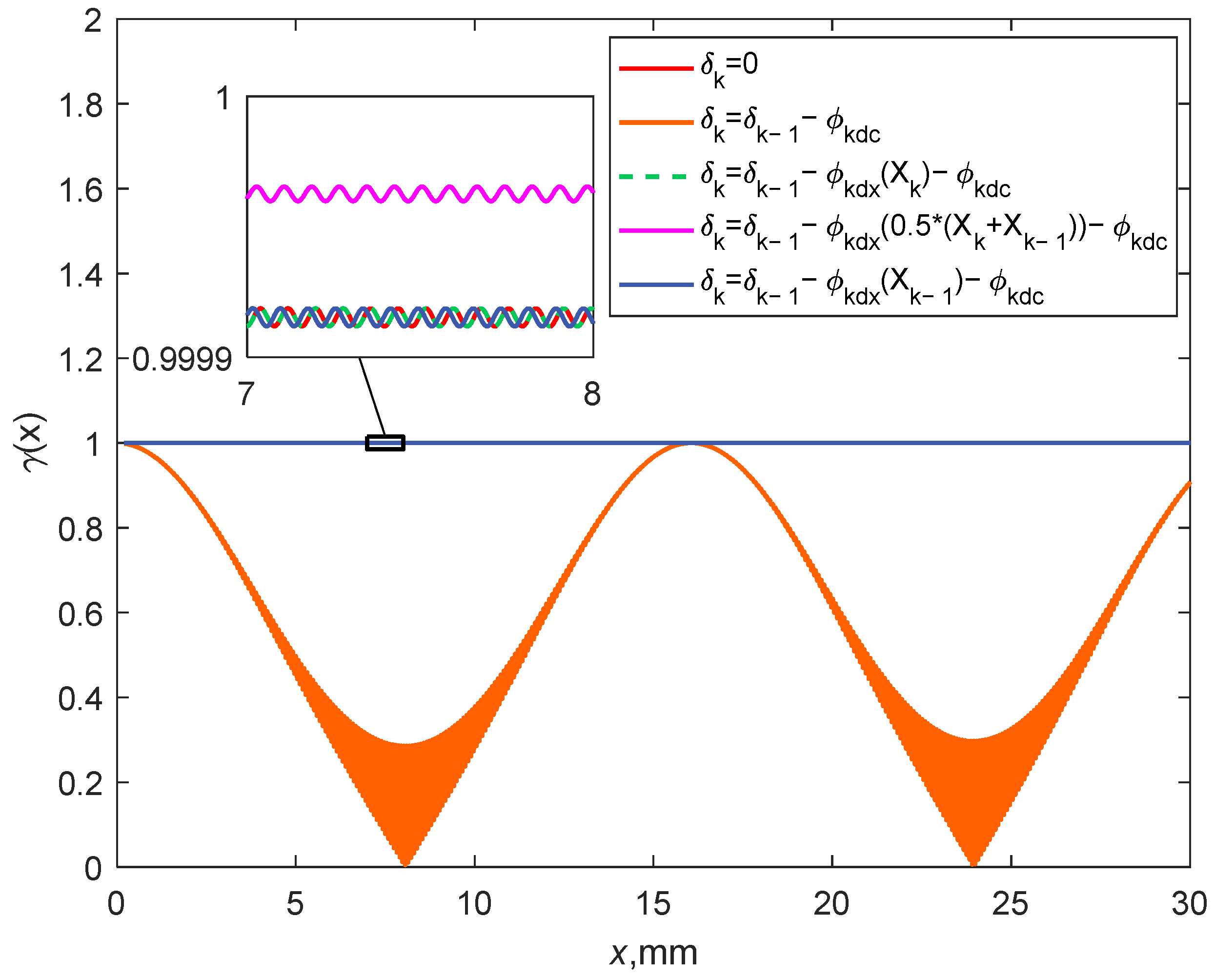
3.2.2. Phase Modulation by Varying fk and δk

Instinctively, the VLS grating can be patterned by directly varying the fringe period according to g(x). In the (k + 1)-th scan, fk is set to the desired density g(Xk) of this scan, and Δk = fkfk−1 = ng1Sk. Sk is not used to modulate the phase in this manner. We chose a constant value of Sc = StepRatio·ω, and Xk = kSc.
The unequal fringe density in the adjacent scans introduces the phase inconsistency. As described in Section 3.2.1, δk cannot compensate for the phase error varying with x. However, with δk in Equation (20), the fringe phase difference between the (k + 1)-th scan and the k-th scan at a certain xcomk coordinate can be compensated.
δ k = δ k 1 φ k d x ( x c o m k ) φ k d c
With f0 = ng0ng1Wg/2, Фe(x) with different δk are shown in Figure 4. Фe(x) is generally a piecewise quadratic polynomial with δk = 0 or δk = δk−1φkdc. The x coordinates of the cusps in Фe(x) coincide with those of the lowest contrasts. Фe(x) with xcomk = (Xk + Xk−1)/2 is close to 0, and Фe(x) with xcomk = Xk and xcomk = Xk−1 have a cumulative characteristic. For small VLS gratings, the cumulative effects can be neglected. However, with increasing the grating size, the cumulative Φe(x) may have a great impact. The Fp2 frequency component in Фe(x) can be acquired by removing the linear polynomial from Фe(x), as shown in Figure 5. The Fp2 frequency components indicate that the phase inconsistences in the adjacent scans are not fully compensated. The peak-to-valley amplitude of the phase fluctuation is close to 2 × 10⁻⁴ rad, which is smaller than 1/30,000 groove period. The grating groove position error caused by the phase fluctuation is smaller than 0.028 nm for the grating example. Compared with the phase errors in nanometer scale caused by the substrate and resist roughness, development, and metrology frame, this small phase fluctuation can usually be neglected for general VLS gratings.
We performed a quadratic polynomial fitting to ΨT(x). The fitting polynomial can be expressed as
Ψ T p ( x ) = 2 π ( a Ψ 2 x 2 + a Ψ 1 x + a Ψ 0 ) = 2 π 0 x g p ( x ) d x + Ψ T p 0
where gp(x) = ngp0 + ngp1(xWg/2) can be treated as the theoretical groove density of the patterned grating. ΨTp0 = 2πaΨ0 is the constant component of ΨTp(x), which has little effect on the characteristics of the grating. The groove density coefficients with different phase compensations are shown in Table 1. The theoretical groove densities gp(x) are close to the desired value, especially gp(x) with xcomk = (Xk + Xk−1)/2.
The exposure contrasts γ(x) are shown in Figure 6. The exposure contrasts are better than 0.99, and γ(x) with xcomk = (Xk + Xk−1)/2 is better than the others. The resist has low-frequency filtering characteristics, so the influence of the Fp2 fluctuation can be neglected [22,23]. The contrast can satisfy the demands of the grating exposure.

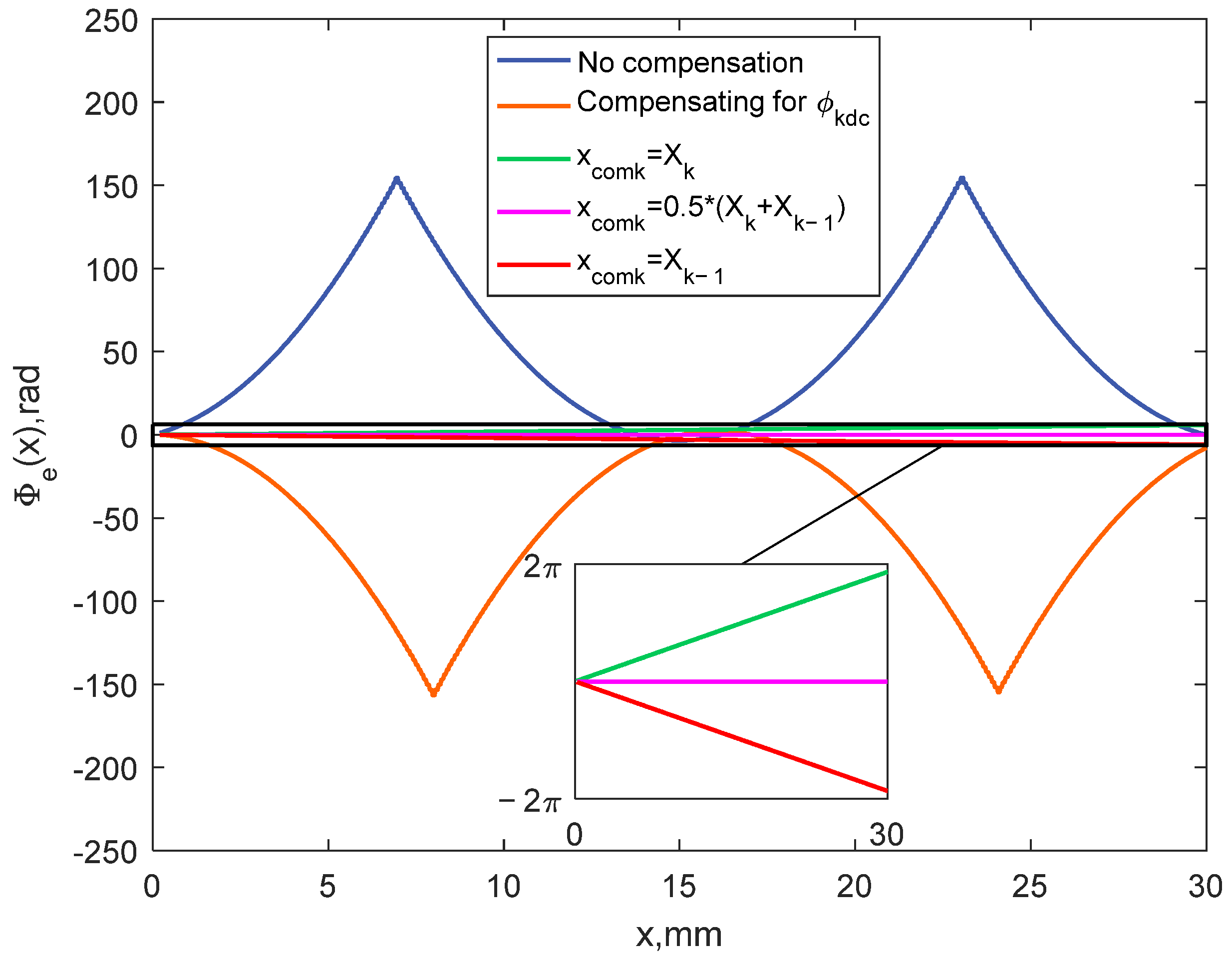
3.2.3. Phase Modulation by Varying fk, Sk and δk

The fringe density fk = g(Xk), and the step size Sk varies according to the fringe density. Here, we set Sk equal to an integer Nsteps multiplied by a variable period value. Nsteps is chosen to be the same constant expressed with Equation (16). The variable period value can be chosen as the fringe period in the adjacent last scan. Sk can be expressed as
S k = N s t e p s / f k 1
The phase difference can also be compensated with δk in Equation (20). With f0 = ng0ng1Wg/2 and the different phase compensation with δk, Φe(x) and γ(x) are shown in Figure 7 and Figure 8, respectively. Except for the condition of δk = δk−1φkdc, Φe(x) is small, and the average contrasts are close to 1. The phase error from adjacent scans still causes Fp2 fluctuations in Φe(x) and γ(x).
As shown in Figure 7, Φe(x) with δk = 0 is coincident with Φe(x) with δk = δk−1φkdx(Xk) − φkdc, which implies that the step size expressed with Equation (22) can compensate for the phase difference at Xk. We assume that the phase difference at xcomk must be compensated, where xcomk is located between Xk−1 and Xk. xcomk can be expressed with Xk−1 and Xk as
x c o m k = X k 1 + r ( X k X k 1 )
where r = (xcomkXk−1)/(XkXk−1) is the ratio. If δk = 0 for all scans, from Equations (9) and (23), the phase difference at xcomk in the k-th scan and (k + 1)-th scan can be expressed as
φ k d ( x c o m k ) = φ k d x ( x c o m k ) + φ k d c = 2 π S k [ ( r f k 1 + ( 1 r ) f k ) ]
From Equation (24), φkd(xcomk) can be compensated with Sk, expressed as
S k = N s t e p s r f k 1 + ( 1 r ) f k
If Sk is other values, such as an actual step size with a stage motion error, δk can be used for phase compensation, which implies that Sk and δk have similar phase modulation effects.
In this manner, the groove density coefficients with different phase compensations are shown in Table 2.

3.3. Parameter Selection for Phase Modulation

We demonstrate three intuitive phase modulation manners and analyze the phase modulation effects of the parameters, including the locked phase δk, fringe density fk, and step size Sk. The results show that the desired phase distribution can be acquired by varying the parameter combinations as follows: (a) fk and δk; (b) fk and Sk; (c) fk, Sk, and δk. These parameters can be selected for phase modulation.
In an actual SBIL system, it is difficult to modulate the exposure phase by only varying Sk because of the stage positioning error. The stage positioning error can be corrected with δk according to the phase compensation relationship. Under this condition, an actual stage can be considered an ideal stage without a positioning error, similar to that in an EP-SBIL system. Therefore, parameter combinations (a) and (c) are applicable to practical applications. Comparing the groove density errors in Table 1 and Table 2, the parameter combination (a) has a better performance, and xcomk = (Xk + Xk−1)/2 is the optimal coordinate for phase compensation.
In addition to the grating example in Section 3.1, other VLS gratings, including another grating in a monochromator (ng0 = 400 L/mm, ng1 = −0.2594 L/mm and Wg = 80 mm) [20] and a grating in a diagnostic spectrometer (ng0 = 600 L/mm, ng1 = −0.7869 L/mm and Wg = 30 mm) [24], are designed for further verification. The results are consistent with the above results. Compared with the existing fabrication methods of VLS gratings, the relative errors of the groove density can satisfy the technical requirements [1,2,3,8,20,24], and the exposure contrast can satisfy the demands for VLS grating fabrication.

4. Discussion

Although Sk and δk have similar phase compensation effects, the results show that parameter combination (a) performs better, and xcomk = (Xk + Xk−1)/2 is the optimal coordinate for phase compensation. The reason for the phenomenon will be discussed.
First, let us focus on the performance differences with different parameter combinations. In parameter combination (b) and (c), Sk varies with fk−1, as expressed in Equation (22). For the VLS grating example in this paper, Sk increases with k. With an increasing Sk, the phase inconsistency from adjacent scans has a greater impact on the phase error and exposure contrast. Therefore, the overall performances with parameter combination (b) and (c) decrease with increasing Sk, and a constant Sk = Sc maintains a consistent performance with combination (a).
Second, the selection of xcomk and the cause of the cumulative characteristic in Φe(x) with xcomk ≠ (Xk + Xk−1)/2 are discussed. As shown in Equation (9), after the phase difference at xcomk is compensated with δk or Sk, the residual phase in φkdx(x) is expressed as
φ k d _ r e s ( x ) = φ k d x ( x ) φ k d x ( x c o m k ) = 2 π Δ k ( x x c o m k )
As shown in Figure 1, the overall phase compensation performance in the x range between Xk−1 and Xk is mainly determined by the k-th scan and (k + 1)-th scan. The overall phase compensation error can be estimated with the integral of φkd_res(x) in the range [Xk−1, Xk] as
I k ( x c o m k ) = X k 1 X k φ k d _ r e s ( x ) d x = 2 π Δ k S k [ ( X k + X k 1 ) / 2 x c o m k ]
Although Equation (27) is not a strict mathematical deduction based on the exposure model, it provides a tool for the analysis. The absolute value of Ik is smaller, and the phase compensation performance is better. If xcomk = (Xk + Xk−1)/2, the best phase compensation performance can be obtained with Ik = 0, and it is not affected by Sk. Therefore, (Xk + Xk−1)/2 is a good selection for xcomk. If xcomk ≠ (Xk + Xk−1)/2, the phase compensation performance degrades with |Ik(xcomk)| > 0. As shown in Figure 4 and Figure 7, Ik(Xk) and Ik(Xk−1) have the same absolute value with opposite signs, which is consistent with the cumulative Φe(x) with different variation directions.

5. Conclusions

In this paper, a mathematical model of the total exposure dose for patterning a VLS grating with VP-SBIL is established, and the phase modulation method of the exposure is proposed. According to the model, the phase modulations in three intuitive manners are calculated, and the phase modulation effects of the parameters, including the locked phase, fringe density, and step size, are analyzed. The phase errors with phase compensation at different coordinates are compared and discussed, and the optimal coordinate for phase compensation is presented. The results show that three parameter combinations can be selected for phase modulation, and the phase modulation performance with the locked phase and the fringe density is better than those with other parameter combinations. The average value of the coordinates in two adjacent scans is the optimal coordinate for phase compensation. The theoretical error between the patterned grating and the desired grating can be controlled within 1e-8, and the requirements of the grating phase distribution and exposure contrast can be satisfied. The proposed exposure dose model and exposure phase modulation method are suitable for VLS planar grating fabrication with VP-SBIL.

Author Contributions

Conceptualization, Y.S. and N.Z.; software, Y.S.; validation, Y.L. and Z.L.; investigation, L.Z.; writing—original draft preparation, Y.S. and N.Z.; writing—review and editing, Y.L.; supervision, L.Z.; project administration, L.Z.; funding acquisition, Y.S., Y.L. and Z.L. All authors have read and agreed to the published version of the manuscript.

Funding

This research was funded by the National Natural Science Foundation of China (NSFC), grant numbers 61905243, 61905245, and 41974210; Scientific Research Project of Education Department of Jilin Province, grant number JJKH20220992KJ; Jilin Province Science and Technology Development Program Project in China, grant number 20200401071GX; and Natural Science Foundation of Jilin Province, grant number 20200201205JC.

Institutional Review Board Statement

Not applicable.

Informed Consent Statement

Not applicable.

Data Availability Statement

The data presented in this study are available on request from the corresponding author.

Acknowledgments

The authors would like to thank the Editor-in-Chief, Editor, and anonymous Reviewers for their valuable reviews.

Conflicts of Interest

The authors declare no conflict of interest.

References

  1. He, W.; Zhang, W.; Meng, F.; Zhu, L. Electron beam lithography inscribed varied-line-spacing and uniform integrated reflective plane grating fabricated through line-by-line method. Opt. Laser Eng. 2021, 138, 106456. [Google Scholar] [CrossRef]
  2. Voronov, D.L.; Warwick, T.; Gullikson, E.M.; Salmassi, F.; Naulleau, P.; Artemiev, N.A.; Lum, P.; Padmore, H.A. Variable line spacing diffraction grating fabricated by direct write lithography for synchrotron beamline applications. Proc. SPIE 2014, 9207, 920706. [Google Scholar]
  3. Reininger, R.; de Castro, A.R.B. High resolution, large spectral range, in variable-included-angle soft X-ray monochromators using a plane VLS grating. Nucl. Instrum. Methods Phys. Res. A 2005, 538, 760–770. [Google Scholar] [CrossRef]
  4. Pu, T.; Cao, F.; Liu, Z.; Xie, C. Deep learning for the design and characterization of high efficiency self-focusing grating. Opt. Commun. 2022, 510, 127951. [Google Scholar] [CrossRef]
  5. Vannoni, M.; Martin, I.F. Absolute, high-accuracy characterization of a variable line spacing grating for the European XFEL soft X-ray monochromator. Opt. Express 2017, 25, 26519. [Google Scholar] [CrossRef] [PubMed]
  6. Shimizu, Y.; Ishizuka, R.; Mano, K.; Kanda, Y.; Matsukuma, H.; Gao, W. An absolute surface encoder with a planar scale of variable periods. Precis. Eng. 2021, 67, 36–47. [Google Scholar] [CrossRef]
  7. Koike, M.; Namioka, T. Plane grating for high-resolution grazing-incidence monochromators: Holographic grating versus mechanically ruled varied-line-spacing grating. Appl. Opt. 1997, 36, 6308–6318. [Google Scholar] [CrossRef] [PubMed]
  8. Jiang, Y. The Research on Design Methods and Fabricating Technology of Varied Line-Space Holographic Plane Grating. Ph.D. Thesis, Chinese Academy of Sciences, Beijing China, 2015. [Google Scholar]
  9. Wang, K.; Zheng, J.; Liu, Y.; Gao, H.; Zhuang, S. Electrically tunable two-dimensional holographic polymer-dispersed liquid crystal grating with variable period. Opt. Commun. 2017, 392, 128–134. [Google Scholar] [CrossRef]
  10. Schattenburg, M.L.; Chang, C.H.; Heilmann, R.K.; Montoya, J.; Zhao, Y. Advanced interference lithography for Nanomanufacturing. Int. Soc. Nanomanufacturing 2006, 44, 441–445. [Google Scholar]
  11. Schattenburg, M.L.; Chen, C.G.; Heilmann, R.K.; Konkola, P.T.; Pati, G.S. Progress towards a general grating patterning technology using phase-locked scanning beams. Proc. SPIE 2002, 4485, 378–384. [Google Scholar]
  12. Pati, G.S.; Heilmann, R.K.; Konkola, P.T.; Joo, C.; Chen, C.G.; Murphy, E.; Schattenburg, M.L. Generalized scanning beam interference lithography system for patterning gratings with variable period progressions. J. Vac. Sci. Technol. B 2002, 20, 2617–2621. [Google Scholar] [CrossRef] [Green Version]
  13. Song, Y.; Liu, Y.; Jiang, S.; Zhu, Y.; Zhang, L.; Liu, Z. Method for exposure dose monitoring and control in scanning beam interference lithography. Appl. Opt. 2021, 60, 2767–2774. [Google Scholar] [CrossRef] [PubMed]
  14. Liu, Z.; Yang, H.; Li, Y.; Jiang, S.; Wang, W.; Song, Y.; Bayanheshig; Li, W. Active control technology of a diffraction grating wavefront by scanning beam interference lithography. Opt. Express 2021, 29, 37066. [Google Scholar] [CrossRef] [PubMed]
  15. Jiang, S.; Lü, B.; Song, Y.; Liu, Z.; Wang, W.; Li, S.; Bayanheshig. Heterodyne period measurement in a scanning beam interference lithography system. Appl. Opt. 2020, 59, 5830–5836. [Google Scholar] [CrossRef] [PubMed]
  16. Heilmann, R.K.; Konkola, P.T.; Chen, C.G.; Pati, G.S.; Schattenburg, M.L. Digital heterodyne interference fringe control system. J. Vac. Sci. Technol. B. 2001, 19, 2342–2346. [Google Scholar] [CrossRef] [Green Version]
  17. Montoya, J. Toward Nano-Accuracy in Scanning Beam Interference Lithography. Ph.D. Thesis, Massachusetts Institute of Technology, Cambridge, MA, USA, 2006. [Google Scholar]
  18. Chen, C.G. Beam Alignment and Image Metrology for Scanning Beam Interference Lithography: Fabricating Gratings with Nanometer Phase Accuracy. Ph.D. Thesis, Massachusetts Institute of Technology, Cambridge, MA, USA, 2003. [Google Scholar]
  19. Konkola, P.T. Design and Analysis of a Scanning Beam Interference Lithography System for Patterning Gratings with Nanometer-Level Distortions. Ph.D. Thesis, Massachusetts Institute of Technology, Cambridge, MA, USA, 2003. [Google Scholar]
  20. Li, C. Variable-Line-Spacing Grating Monochromators Design and Key Techniques. Ph.D. Thesis, University of Science and Technology of China, Hefei, China, 2014. [Google Scholar]
  21. Jiang, S.; Bayanheshig; Li, W.; Song, Y.; Pan, M. Effect of period setting value on printed phase in scanning beam interference lithography system. Acta Opt. Sin. 2014, 34, 0905003. [Google Scholar] [CrossRef]
  22. Dill, F.H.; Hornberger, W.P.; Hauge, P.S.; Shaw, J.M. Characterization of positive photoresist. IEEE Trans. Electron Devices 1975, 22, 445–452. [Google Scholar] [CrossRef]
  23. Han, J.; Bayanheshig; Li, W.; Kong, P. Profile evolution of grating masks according to exposure dose and interference fringe contrast in the fabrication of holographic grating. Acta Opt. Sin. 2012, 32, 0305001. [Google Scholar] [CrossRef]
  24. Jiang, Y.; Bayanheshig; Yang, S.; Zhao, X.; Wu, N.; Li, W. Study on the effects and compensation effect of recording parameters error on imaging performance of holographic grating in on-line spectral diagnose. Spectrosc. Spectr. Anal. 2016, 36, 857–863. [Google Scholar]
Figure 1. The exposure doses in three adjacent scans.
Applsci 12 07946 g001
Figure 2. Phase error under the condition δk = Фg(Xk).
Applsci 12 07946 g002
Figure 3. Exposure contrast and difference in Фe(x) under the condition δk = Фg(Xk).
Applsci 12 07946 g003
Figure 4. Phase error under the condition of fk = g(Xk) with different δk.
Applsci 12 07946 g004
Figure 5. Phase error fluctuation under the condition of fk = g(Xk) with different δk.
Applsci 12 07946 g005
Figure 6. Exposure contrast under the condition of fk = g(Xk) with different δk.
Applsci 12 07946 g006
Figure 7. Phase error under the condition of fk = g(Xk) and Sk = Nsteps/fk−1 with different δk.
Applsci 12 07946 g007
Figure 8. Exposure contrast under the condition of fk = g(Xk) and Sk = Nsteps/fk−1 with different δk.
Applsci 12 07946 g008
Table 1. gp(x) under the condition of fk = g(Xk) and phase compensation with δk.
xcomkgp(x) CoefficientsRelative Errors of gp(x) Coefficients
ngp0, L/mmngp1, L/mm2ε(ng0) = |ngp0ng0|/ng0ε(ng1) = |ngp1ng1|/ng1
Xk1200.0311−0.77832.5943 × 10−5<1 × 10⁻⁸
(Xk + Xk−1)/21200.0000−0.7783<1 × 10−8<1 × 10⁻⁸
Xk−11199.9689−0.7783−2.5943 × 10⁻⁵<1 × 10⁻⁸
Table 2. gp(x) under the condition of fk = g(Xk) and phase compensation with Sk.
xcomkgp(x) CoefficientsRelative Errors of gp(x) Coefficients
ngp0, L/mmngp1, L/mm2ε(ng0)ε(ng1)
Xk1200.0311−0.77832.5943 × 10−5−2.5946 × 10⁻⁵
(Xk + Xk−1)/21200.0000−0.7783<1 × 10−8<1 × 10⁻⁸
Xk−11199.9689−0.7783−2.5943 × 10−52.5946 × 10−5
Publisher’s Note: MDPI stays neutral with regard to jurisdictional claims in published maps and institutional affiliations.

