
Novel Abrasive-Impregnated Pads and Diamond Plates for the Grinding and Lapping of Single-Crystal Silicon Carbide Wafers


1
Department of Mechanical Engineering, National Chin-Yi University of Technology, Taichung 41170, Taiwan
2
Graduate Institute of Precision Manufacturing, National Chin-Yi University of Technology, Taichung 41170, Taiwan
*
Author to whom correspondence should be addressed.
Appl. Sci. 2021, 11(4), 1783; https://doi.org/10.3390/app11041783
Submission received: 19 January 2021
/
Revised: 5 February 2021
/
Accepted: 9 February 2021
/
Published: 17 February 2021
(This article belongs to the Special Issue 2021 Smart Manufacturing on Production System, Quality Assurance, Process Optimization, and Digital Modeling)
Abstract
:In this study, special ceramic grinding plates impregnated with diamond grit and other abrasives, as well as self-made lapping plates, were used to prepare the surface of single-crystal silicon carbide (SiC) wafers. This novel approach enhanced the process and reduced the final chemical mechanical planarization (CMP) polishing time. Two different grinding plates with pads impregnated with mixed abrasives were prepared: one with self-modified diamond + SiC and a ceramic binder and one with self-modified diamond + SiO2 + Al2O3 + SiC and a ceramic binder. The surface properties and removal rate of the SiC substrate were investigated and a comparison with the traditional method was conducted. The experimental results showed that the material removal rate (MRR) was higher for the SiC substrate with the mixed abrasive lapping plate than for the traditional method. The grinding wear rate could be reduced by 31.6%. The surface roughness of the samples polished using the diamond-impregnated lapping plate was markedly better than that of the samples polished using the copper plate. However, while the surface finish was better and the grinding efficiency was high, the wear rate of the mixed abrasive-impregnated polishing plates was high. This was a clear indication that this novel method was effective and could be used for SiC grinding and lapping.
1. Introduction
Single-crystal silicon carbide (SiC) is a new high-powered, next-generation semiconductor material that can be used for chip production. This material has several important features that make it better than other materials for many purposes. For example, it has high dielectric strength against field collapse, high saturated electron drift velocity, high mechanical strength, great thermal conductivity, and excellent chemical stability. However, its chemical inertness and high strength make single-crystal silicon carbide very difficult to machine [1,2,3,4,5]. The material was used during the early development of the LED industry, and the flattening of SiC wafers was problematic from the very start. Grinding and polishing are generally done using a free-abrasive slurry against a copper or cast iron lapping plate. However, this is not very efficient, as it takes a long time and the cost is high. The removal of material during flattening in this way requires three-body wear in which material is removed by abrasive particles rolling and sliding in a slurry between the SiC wafer and the hard plate. The material removal rate by three-body wear is about one-tenth of that achievable by two-body wear. Such low processing efficiency is due to the fact that the abrasive particles spend 90% of the time rolling and only 10% sliding [6]. Mechanical polishing (MP) [7] and chemical mechanical planarization [8,9,10] are core technologies used in semiconductor manufacturing, but the material removal rate (MRR) is very low and takes a long time. Any methods that can improve performance should therefore be investigated.
Several important studies have recently been carried out on diamond abrasive grinding. Park et al. [11] estimated the rate of material removal by lapping sapphire wafers. Their three-body wear model used a diamond slurry on metal–resin-bound lapping plates made with copper, aluminum, or zinc powder. Metal–resin plates combined with abrasives were also used. Two-body wear experiments were also performed using fixed diamond abrasives in a platen dressed with a low concentration of Al2O3 slurry. Extensive tests were carried out, the basic purpose of which was to find an optimum lapping process for sapphire wafers. Lapping was done under different loads and at different rotation speeds and times. Gao et al. [12] used arc diamond grinding wheels in a dressing process to investigate wear. Next, they studied the efficiency of different abrasives and bonding agents on the arc grinding wheel dressing process. The convex nonspherical SiC formed by the dressed arc diamond grinding wheels revealed that the dressing by both the resin and metal bonding agents was efficient and accurate. In addition, the diamond abrasives were distributed more evenly in the arc grinding wheels, and more sharp diamond points were exposed after dressing. Zhang et al. [13] used a new type of ultraprecise diamond grinding wheel to polish cadmium–copper nanofilm. Their results showed non-subsurface damage and an undeformed nanocutting intersecting surface. Puttick et al. [14] found that there was a transition from a brittle to a ductile mode in the single-edge cutting of single-crystal silicon material. This phenomenon occurred at a critical cutting thickness. In other words, at some stage, the cutting process caused plastic deformation, not brittle fractures. Huo et al. [15] proposed a method for grinding hard and brittle material with nanodiamond grinding wheels with three different diamond grits in a ceramic bonded wheel, in which deionized (DI) water was used as the grinding slurry. The result clearly showed that double-side grinding could replace mechanical polishing. Bifano et al. [16] presented a plastic deformation theory for hard–brittle material which revealed that the energy needed for ductile grinding was lower than what could cause brittle fractures at a specific critical depth. This result indicated that the material removal mechanism involved was ductile grinding and that decreasing the cutting depth could transform brittle grinding into ductile grinding. This could reduce the depth of damage and the surface roughness and provide a finer polish. Gao et al. [17] proposed that diamond abrasive grinding is the most common method used in silicon wafer manufacturing but that edge cutting is always needed to dice the wafer. The study was mainly an investigation of the edge cutting of silicon wafers with a diamond grinding wheel. Experiments included the use of different diamond grits, and both up-grinding and down-grinding were used. The size of the abrasive, the feed rate, and the wafer thickness all influenced the crack effect of the blade. The critical thickness results showed that this was higher in up-grinding than in down-grinding. The use of less abrasive and a lower feed could reduce cracking at the cutting edge; however, with thicker wafers, the cutting crack size during down-grinding was higher than that during up-grinding. Velden et al. [18] mentioned in their study that the 3M company uses polishing pads with fixed abrasives, as well as a nonpolishing slurry CMP. The polishing pad is impregnated with abrasives which promote grinding efficiency, and the surface flatness is 3 times better than in a free-abrasive process. Enomoto et al. [19] proposed a traditional grinding model with free abrasives; however, the cost was high, and it also seriously harmed the environment. They investigated a fixed abrasive grinding model and developed a spiral-structured fixed cerium oxide (ceria) abrasive polishing pad that was more environmentally friendly.
In this study, three kinds of grinding pads impregnated with mixed abrasives, along with self-made lapping plates, were used for the lapping of single-crystal SiC wafers. All were shown to enhance performance and reduce polishing time. Three combinations of abrasives were used to impregnate the different types of polishing pads: Type 1, consisting of 50% industrial monocrystalline diamond grit and 10% green silicon carbide (GC); Type 2, consisting of 50% self-modified diamond and 10% GC; and Type 3, consisting of 16.67% self-modified diamond, 16.67% SiO2, and 10% GC. All were compressed under high pressure into pads with a ceramic binder and sintered at 700 °C. The surface characteristics and removal rate of the SiC wafers polished with these newly developed polishing pads were examined and compared with the results from conventional lapping using a copper plate.
2. Experimental Details
There are large variations in the surface roughness and flatness of SiC wafers sliced by a diamond wire saw. It takes a long time just to remove the original roughness and slicing marks using chemical mechanical polishing. Therefore, three sequential steps are normally taken for the polishing process of SiC wafers, as shown in Figure 1. The first step involves grinding with 6 μm diamond powder for 30 min. After this, numerous brittle fractured pits will still remain on the wafer surface. In the next step, 3 μm diamond powder is used to lap the wafer for 30 min. The final chemical mechanical polishing generates the best surface finish. In this study, the SiC grinding and lapping steps are presented and described in detail below.
2.1. Preparing the SiC Wafer
2.2. The Grinding Processes
Figure 3a is a flow diagram of the steps used in the fabrication of the grinding plates impregnated with diamond grit. The process was as follows: First, the bonding resin agent and different abrasives were prepared and mixed. Second, the abrasive mixture was placed in a mold and compressed at a temperature of 700 °C and with a pressure of 100 to form an abrasive pad with a diameter of 38 mm and a thickness of 7 mm. Third, the aluminum plate used to hold the grinding head was machined from 7075 aluminum alloy (the dimensions are shown in Figure 3b). The milled recesses were 2 mm deep, leaving 5 mm of the abrasive pads protruding. Fourth, the pads were fixed into the recesses using an epoxy resin adhesive, and heat and pressure were applied to cure the adhesive. Finally, a grinder/polisher machine was adopted to trim the grinding plates. The grinder/polisher was manufactured by TOP TECH company in Taiwan and the type is PLATO-FSR. Three different grinding plates were fabricated, as shown in Table 1: Type 1, consisting of 50% industrial monocrystalline diamond and 10% green silicon carbide (GC); Type 2, consisting of 50% self-modified diamond and 10% GC; and Type 3, consisting of 16.67% self-modified diamond + 16.67% SiO2 and 10% GC. All were compressed into pads under high pressure with a ceramic binder and sintered at 700 °C. The modified diamond abrasives were prepared by mixing with Fe3O4, and sintering was performed in a furnace at 500–800 °C to produce a diamond abrasive material with a porous structure, as shown in Figure 4 and Figure 5. The ball milling machine used in this study was manufactured by Chemist company in Taiwan and the type is BLT-150D. The maximum roller speed is 700 rpm and the roller size is 380 mm. It has three rollers. In this study, the single-crystal diamond, as shown in Figure 5a, was transformed into a porous diamond (Figure 5b) after reforming.
2.3. The Lapping Processes
The three stages included fabrication of the self-made lapping plate. First, the grooved plate was designed using CAD software (SolidWorks 2015, Dassault Systemes S.A. Inc in USA.), and a mold was made by CNC (Machine Center, YCM Inc., NSV series in Taiwan). Second, the hydrogenated diamond particles were prepared using heat treatment, and dispersion was uniform within the resin matrix. Third, the resin and diamond were mixed and poured into a mold, which was then compressed to form a flat disc. Finally, the mold and plate were separated to obtain a 2-mm-thick pad with a diameter of 305 mm, as shown in Figure 6a. In the experiments, a traditional copper plate was used. Its performance is shown in Figure 6b. The names of four types of lapping processes, used in the investigations, are shown in Table 2.
2.4. The Experiment Processes and Measurements
A modified variable-speed polishing and dressing machine was used for the grinding and lapping experiments, as shown in Figure 7. During grinding and lapping, a power head applied a specific load (10–80 N) to a SiC wafer with a diameter of 100 mm and a thickness of 0.5 mm, which rotated at 80 rpm. A constant flow of slurry at 150 mL/h was used; the load applied to the plate was about 30 N, and the table disk rotated at 80 rpm. During conditioning, the diamond pad conditioner was attached to a moving head. The oscillation speed of the conditioner and the applied load was fixed. After the SiC substrate polishing process was completed, its surface roughness value was measured using a Zygo NewView 8300 interferometer (AMETEK, Inc. in UK) and white light (WLI) by a noncontact 3D optical method with a root-mean-square (RMS) repeatability of 0.01 nm and a measuring range of more than 20 mm. The measurement area of each image was 86 × 86 μm. The surface roughness value for each workpiece was taken as the average of nine measurements. The thickness of the SiC samples was measured before and after the polishing process, and the accuracy was 0.1 μm.
2.5. Theoretical Analysis
There are various models that can be used for different chemical mechanical polishing processes. The most basic equation is Preston’s equation, which has a profound effect on the parameters used in the polishing process and the material removal rate. Generally, the amount of material removal V is expressed by the Preston equation as [20]
where c is the polishing condition constant, p is the applied pressure, v is the relative speed between the polishing disc and the workpiece, and t is the processing time. However, the material removal rate (MRR) is proportional to the product of the applied pressure and the relative speed and can be written as
In addition, the total number of abrasive particles N on the surface of the polishing pad can be calculated by the following equation [21]:
where is the contact area. If the abrasive particles are considered to be evenly distributed, the following equation can be used:
where k is the correlation coefficient of CMP. The polishing rate and pressure in Equation (4) have a nonlinear relationship.
3. Results and Discussion
3.1. The Wear Rate by Grinding
Wear rate is one of the most important factors influencing the surface condition and cost of a grinding tool. The amount of grinding surface that is removed per unit time is referred to as the wear rate and is measured in μm/min and calculated as the amount of grinding surface over the time taken. The diamond dresser used in this study was a Kinik brazed diamond disk with a grit size of 150–180 μm (see Figure 7). The parameters used for dressing were a loading pressure of 60 N, a clockwise dresser rotation speed of 100 rpm, a clockwise lapping plate rotation of 40 rpm, a dressing time of 10 min, and a DI water flow rate of 250 mL/h. Figure 8 shows the variation of the wear rate between the three different diamond plates. The wear rate of Grinding-3 was about 7.6 μm/min, which was higher than for Grinding-1 and Grinding-2, which had wear rates of around 5.2 and 5.6 μm/min, respectively. The wear rates of Grinding-1 and Grinding-2 could be reduced by 31.6% and 26.3%, respectively.
To find out why the wear rate for the 6 µm diamond grit was so high, the Rockwell hardness (WiZhard HR511, Mitutoyo Inc. in Japan) and surface structure of the different diamond grinding plates were investigated. The analysis showed that the hardness of Grinding-3 was HRA 45, which was much lower than that of Grinding-1 and Grinding-2 (HRA 61 and HRA63, respectively). The resulting difference in hardness could explain why the wear rate was so different.
3.2. Material Removal Rate and Surface Roughness of the SiC Wafers Achieved by Grinding
The material removal rate of SiC wafers is very important in grinding processes. Therefore, in this study, the material removal rates of different diamond grinding plates under the same experimental conditions were investigated. Figure 9a shows the material removal rate of the SiC wafer achieved by the different diamond grinding plates at the same rotation speed and pressure. The material removal rate is defined as the thickness removed in units of time. The figure shows that the material removal rate for Grinding-2 was 2.2 μm/min. This was higher than the rates for Grinding-1 and Grinding-3 (1.5 μm/min and 1.8 μm/min, respectively). The material removal rates of Grinding-1 and Grinding-3 could be enhanced by 31.8% and 18.2%, respectively. Figure 9b also shows the variation in the grinding ratio using different diamond grinding plates. As can be seen in the figure, the grinding ratio of Grinding-1 was about 2.4, which was 14.3% and 50% higher than the ratios of 2.1 and 1.6 for Grinding-2 and Grinding-3, respectively. In practice, a lower grinding ratio is not always desirable unless consumption of the grinding surface is the chief concern, in which case Grinding-1 would be recommended. The reason for the high grinding ratio was the strength of the grit binder. This also meant that worn-out diamond grit would remain held in place by the binder and that new sharp edges would not be exposed. The retention of the blunt diamond grit would result in rubbing, rather than a cutting action, and the material removal rate would go down. This was an interesting observation and may have been the result of the porous nature of Grinding-2 and Grinding-3, which allowed more self-sharpening and increased the fresh diamond grit cutting efficiency. On the other hand, Grinding-1 could hold the diamond grit more strongly and there was less self-sharpening (see Figure 10). This reduced the cutting ability and could even cause deterioration of the wafer surface. Grinding wheel wear is generally correlated with the amount of workpiece material ground by the grinding ratio parameter, which is defined as the volume of material removed divided by the volume of wheel wear. In practice, the grinding ratio varies widely and can be between 1 and 200 or even more. The grinding ratio depends on the type of wheel and the workpiece and process parameters, but the grinding ratio is usually less than 1 for materials that are difficult to cut. Images of the surface roughness measured by the Zygo interferometer are shown in Figure 11 and Figure 12. The surface of the wafer lapped by Grinding-1 was much rougher than that produced by Grinding-3. For Grinding-1, the Sa value was about 41 nm and the Sz value was about 1129 nm. For Grinding-2, Sa was about 37 nm and Sz was about 832 nm. These were markedly higher than the Sa of about 25 nm and the Sz of about 651 nm achieved with Grinding-3. Clearly, the reason for these differences was that Grinding-3 had better self-sharpening action. However, this higher lapping plate consumption led to a shorter working life, which is a problem that needs to be solved.
3.3. Material Removal Rate and Surface Roughness Achieved by Lapping
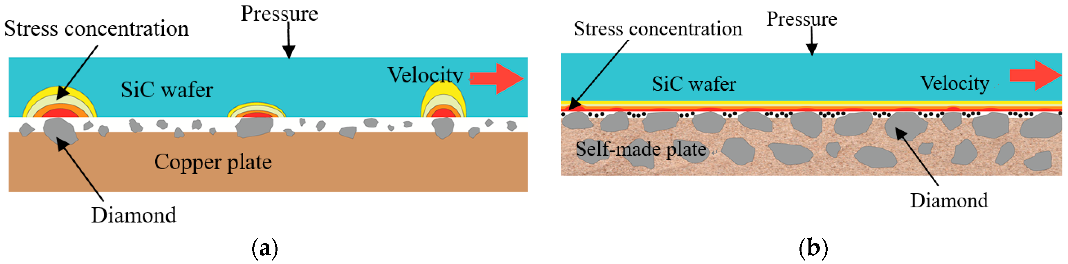
Figure 13 shows variations in the average removal rates of the SiC when using different plates. The MRR for Lapping-2 (copper plate + self-modified diamond slurry) was 1.9 µm/min, which was higher than the 1.7 µm/min for Lapping-1 (copper plate + industrial diamond slurry). As shown in the figure, the SiC removal rate was higher for Lapping-1 and Lapping-2 (copper plate) than for Lapping-3 and Lapping-4 (resin plate impregnated with diamond), which were 0.96 and 1.5 µm/min, respectively, as expected. Figure 14 shows the Sa and the root-mean-square roughness (Sz) of the SiC samples polished by the conventional copper plate and the resin plate impregnated with diamond. According to these measurements, as shown in Figure 15, the average Sa and Sz values of the SiC samples after Lapping-1 were 22 and 617 nm, while those for Lapping-2 were about 21 and 543 nm, respectively. The average Sa and Sz values for Lapping-3 were approximately 4.75 and 218 nm, respectively, and these values for Lapping-4 were 4.6 and 395 nm, respectively. The surface finish of the samples polished by the resin diamond plates was much better than what could be achieved with the copper plate. Luo et al. [22] suggested that sharp diamond grit particles will remain on the plate surface and cause the deep scratches and pits found on the polished wafer surface. To determine the actual situation, scanning electron microscopy (SEM) was used to examine the surface of the lapping plate (see Figure 16). It was discovered that the residual diamond abrasive particles on the copper plate could not be removed after diamond disk dressing of the copper plate. This result could be due to the fact that the two-body lapping process could easily scratch the SiC wafer. The self-made lapping plate did not have diamond particles adhering to it, and the SiC substrate had fewer scratches and a better surface roughness value, as shown in Figure 17. When using a traditional metal lapping plate, abrasive particles could easily fall from the plate and create an uneven stress distribution resulting in a poor surface roughness value, as shown in Figure 18 [23]. Tsai et al. [24] pointed out that the excellent self-sharpening ability of the lapping plates causes even material removal with the least surface roughness.
4. Conclusions
In this study, novel grinding and lapping plates were used to polish the surface of single-crystal SiC wafer surfaces. The abrasive-impregnated grinding plates used included self-modified diamond + SiC and self-modified diamond + SiO2 + Al2O3+ SiC bonded in ceramic. A resin-bonded lapping plate with embedded micro-sized diamond grit was also developed and used in this study. The surface characteristics and the material removal rate (MRR) of the SiC sample wafers polished using the developed techniques were examined and compared with those obtained using conventional grinding and lapping using a copper plate. The MRR of the SiC from the wafer surface with the mixed abrasive-impregnated grinding pads was higher and gave better surface finish and grinding efficiency than those achievable with conventional grinding tools. However, a higher lapping plate consumption led to a shorter working life for Grinding-3. This presented a problem that will have to be addressed. The SiC removal rate using a copper plate was found to be higher than that of the resin/diamond plate. However, the surface finish of the samples polished using the resin/diamond plate was much better than what could be achieved using the copper plate. This shortened the time taken for the chemical mechanical polishing process. The results obtained in this study may help with the development of more efficient grinding and lapping methods for SiC wafers.
Author Contributions
Conceptualization, M.-Y.T.; data curation, K.-Y.L.; formal analysis, K.-Y.L. and S.-Y.J.; funding acquisition, M.-Y.T.; investigation, M.-Y.T.; methodology, M.-Y.T.; project administration, M.-Y.T.; software, S.-Y.J.; validation, K.-Y.L. and S.-Y.J.; visualization, S.-Y.J.; writing—original draft, M.-Y.T.; writing—review & editing, K.-Y.L. All authors have read and agreed to the published version of the manuscript.
Funding
This research received no external funding.
Acknowledgments
The author gratefully acknowledges the financial support provided for this study by the Ministry of Science and Technology of Taiwan under the Grant MOST 109-2622-E167-010-CC3 and 109-2634-F-009-031.
Conflicts of Interest
The authors declare no conflict of interest.
References
- Zhou, Y.; Pan, G.; Zou, C.; Wang, L. Chemical Mechanical Polishing (CMP) of SiC Wafer Using Photo-Catalyst Incorporated Pad. J. Solid State Sci. Technol. 2017, 6, 603–608. [Google Scholar] [CrossRef]
- Fan, D. A study on the polishing mechanism of silicon carbide (SiC) optic surface. Adv. Mater. Res. 2011, 337, 474–478. [Google Scholar] [CrossRef]
- Shi, X.L.; Pan, G.S.; Yan, Z.; Gu, Z.H.; Hua, G.; Zou, C.L. Characterization of colloidal silica abrasives with different sizes and their chemical–mechanical polishing performance on 4H-SiC (0001). Appl. Surf. Sci. 2014, 307, 414–427. [Google Scholar] [CrossRef]
- Zhou, Y.; Pan, G.S.; Shi, X.L.; Zhang, S.M.; Gong, H.; Luo, G.H. Effects of ultra-smooth surface atomic step morphology on chemical mechanical polishing (CMP) performances of sapphire and SiC wafers. Tribolgy Int. 2015, 87, 145–150. [Google Scholar] [CrossRef]
- Ho, J.K.; Huang, C.Y.; Tsai, M.Y.; Tsai, C.C. Investigation of Polishing Pads Impregnated with Fe and Al2O3 Particles for Single-Crystal Silicon Carbide Wafers. Appl. Sci. 2016, 6, 89. [Google Scholar] [CrossRef] [Green Version]
- Harshaand, P.; Tewari, U.S. Two-body and three-body abrasive wear behaviour of polyaryletherketone Composites. Polym. Test. 2003, 22, 403–418. [Google Scholar] [CrossRef]
- Ke, X.; Qiu, L.; Wang, C.; Wang, Z. Tentative Investigations on Reducing the Edge Effects in Pre-Polishing the Optics. Appl. Sci. 2020, 10, 5286. [Google Scholar] [CrossRef]
- Zhao, T.; Yuan, J.; Deng, Q.; Feng, K.; Zhou, Z.; Wang, X. Contrast Experiments in Dielectrophoresis Polishing (DEPP)/Chemical Mechanical Polishing (CMP) of Sapphire Substrate. Appl. Sci. 2019, 9, 3704. [Google Scholar] [CrossRef] [Green Version]
- Cao, L.; Zhang, X.; Yuan, J.; Guo, L.; Hong, T.; Hang, W.; Ma, Y. Study on the Influence of Sapphire Crystal Orientation on Its Chemical Mechanical Polishing. Appl. Sci. 2020, 10, 8065. [Google Scholar] [CrossRef]
- Chen, C.C.A.; Li, J.C.; Liao, W.C.; Ciou, Y.J.; Chen, C.C. Dynamic Pad Surface Metrology Monitoring by Swing-Arm Chromatic Confocal System. Appl. Sci. 2021, 11, 179. [Google Scholar] [CrossRef]
- Park, J.G.; Kim, H.M.; Park, G.H.; Seo, Y.G.; Moon, D.J.; Cho, B.J. Comparison between sapphire lapping processes using 2-body and 3-body modes as a function of diamond abrasive size. Wear 2015, 332–333, 794–799. [Google Scholar]
- Guo, B.; Chen, B.; Zhao, Q. On-machine precision form truing of arc-shaped diamond wheels. J. Mater. Process. Technol. 2015, 223, 65–74. [Google Scholar]
- Zhang, Z.; Song, Y.; Xu, C.; Guo, D. A novel model for undeformed nanometer chips of soft-brittle Hg Cd Te films induced by ultrafine diamond grits. Scr. Mater. 2012, 67, 197–200. [Google Scholar] [CrossRef]
- Puttick, K.E.; Rudman, M.R.; Smith, K.J.; Franks, A.; Lindsey, K. Single-point diamond machining of glasses. Proc. R. Soc. Lond. 1989, 426, 19–30. [Google Scholar]
- Huo, F.W.; Guo, D.M.; Kang, R.K.; Feng, G. Nanogrinding of SiC wafers with high flatness and low subsurface. Trans. Nonferrous Met. Soc. China 2012, 22, 3027–3033. [Google Scholar] [CrossRef]
- Bifano, T.G. A Dow and, RO Scattergood. Ductile-regime grinding: A new technology for machining brittle materials. J. Eng. Ind. 1991, 113, 184–189. [Google Scholar] [CrossRef]
- Gao, S.; Kang, R.; Dong, Z.; Zhang, B. Edge chipping of silicon wafers in diamond grinding. Int. J. Mach. Tools Manuf. 2013, 64, 31–37. [Google Scholar] [CrossRef]
- Velden, P. Chemical mechanical polishing with fixed abrasives using different sub pads to optimize wafer uniformity. Microelectron. Eng. 2000, 50, 41–46. [Google Scholar] [CrossRef]
- Enomoto, T.; Satake, U.; Fujita, T.; Sugihara, T. Spiral-structured fixed-abrasive pads for glass finishing. Cirp Ann. Manuf. Technol. 2013, 62, 311–314. [Google Scholar] [CrossRef]
- Preston, F.W. The theory and design of plate glass polishing machines. J. Soc. Glass Technol. 1927, 11, 214–256. [Google Scholar]
- Raghavan, S.; Opila, R.L.; Zhang, L. Chemical Mechanical Planariarization in Integrated Circuit Device Manufacturing; The Electrochemical Society: Pennington, NJ, USA, 1998. [Google Scholar]
- Luo, Q.F.; Lu, J.; Xu, X.P. A comparative study on the material removal mechanisms of 6H-SiC polished by semi-fixed and fixed diamond abrasive tools. Wear 2016, 350–351, 99–106. [Google Scholar] [CrossRef]
- Doi, T.K.; Seshimo, K.; Yamakzi, T.; Ohtsubo, M. Building of super high-efficiency processing technology based on innovative concept (Establishment of effective polishing process of SiC substrate using Dilatancy pad tool with bowl feed method). Trans. JSME (Jpn.) 2015, 81, 824–830. [Google Scholar]
- Tsai, M.Y.; Lin, Y.F.; Lin, G.F. Development of Combined Diamond Impregnated Lapping Plates. Sens. Mater. 2018, 30, 11–16. [Google Scholar] [CrossRef]
Figure 1.
SiC wafer polishing steps.

Figure 2.
(a) 4H-SiC wafer; (b) surface interferometer image.
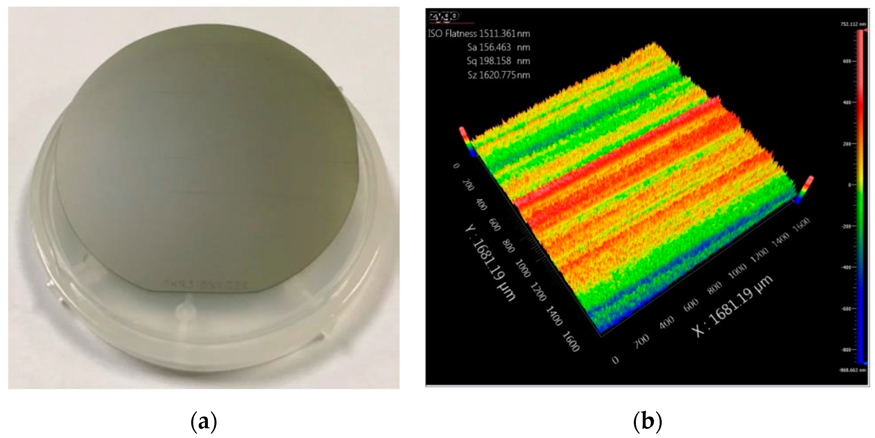
Figure 3.
Diamond polishing plate: (a) the process of making a diamond polishing plate; (b) the diamond polishing plate and pads.
Figure 3.
Diamond polishing plate: (a) the process of making a diamond polishing plate; (b) the diamond polishing plate and pads.

Figure 4.
Preparing the self-modified diamond grit.
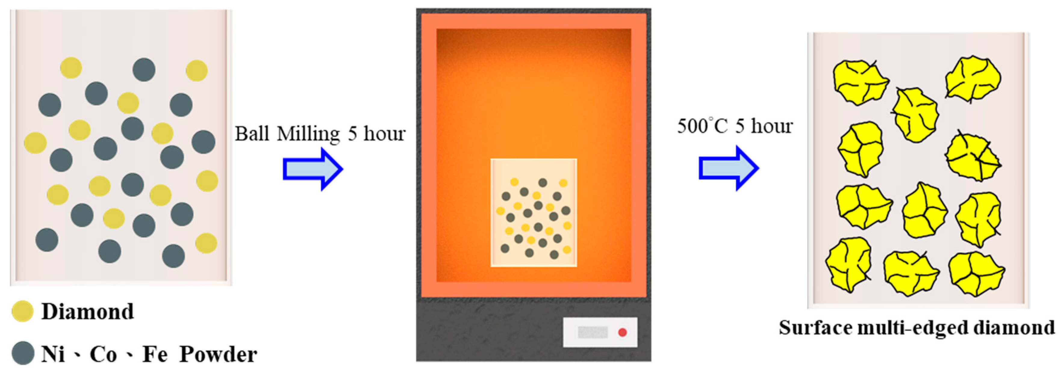
Figure 5.
(a) Original diamond grit; (b) porous diamond grit structure.
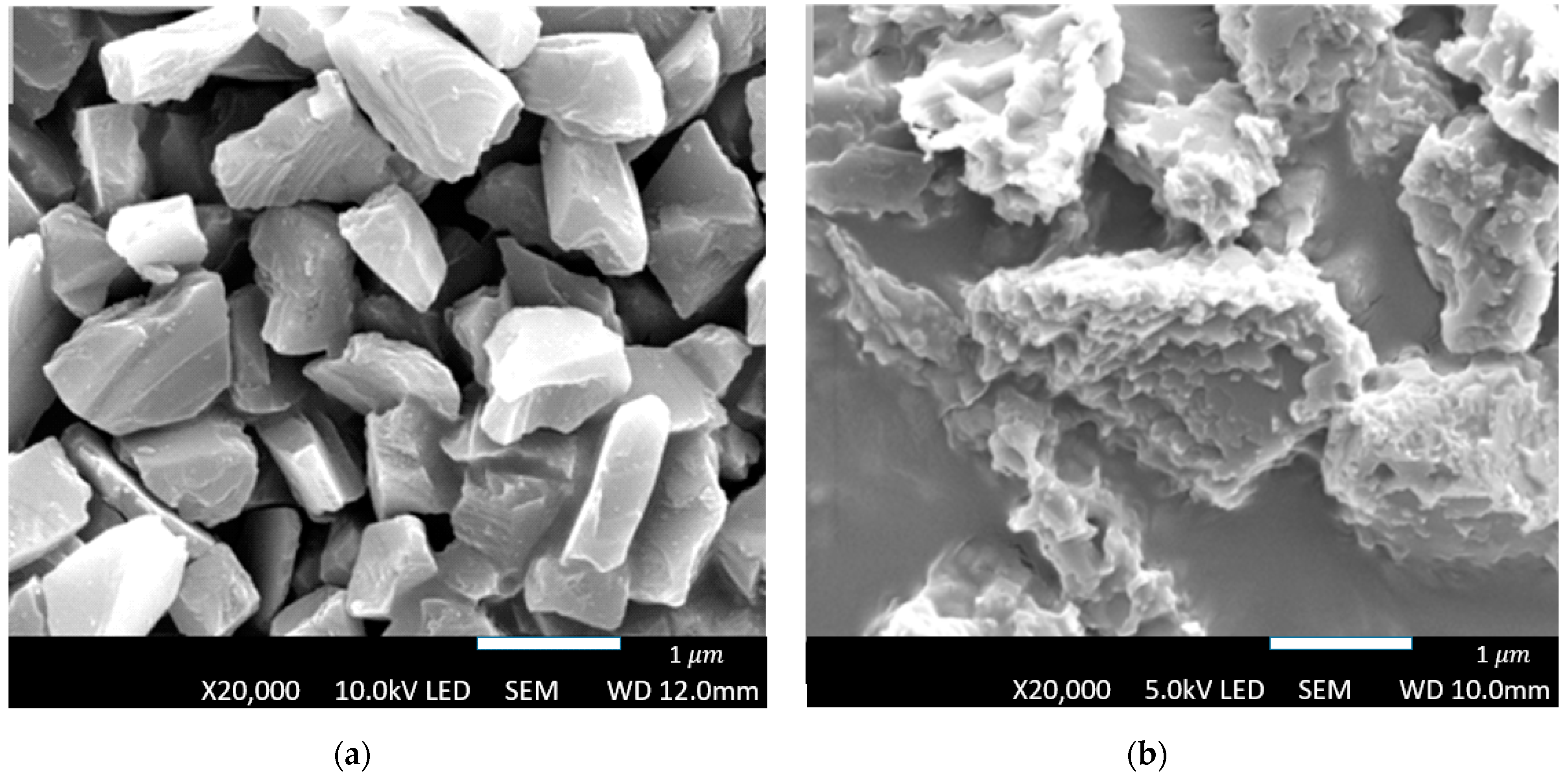
Figure 6.
(a) Self-made lapping plate; (b) traditional copper plate.
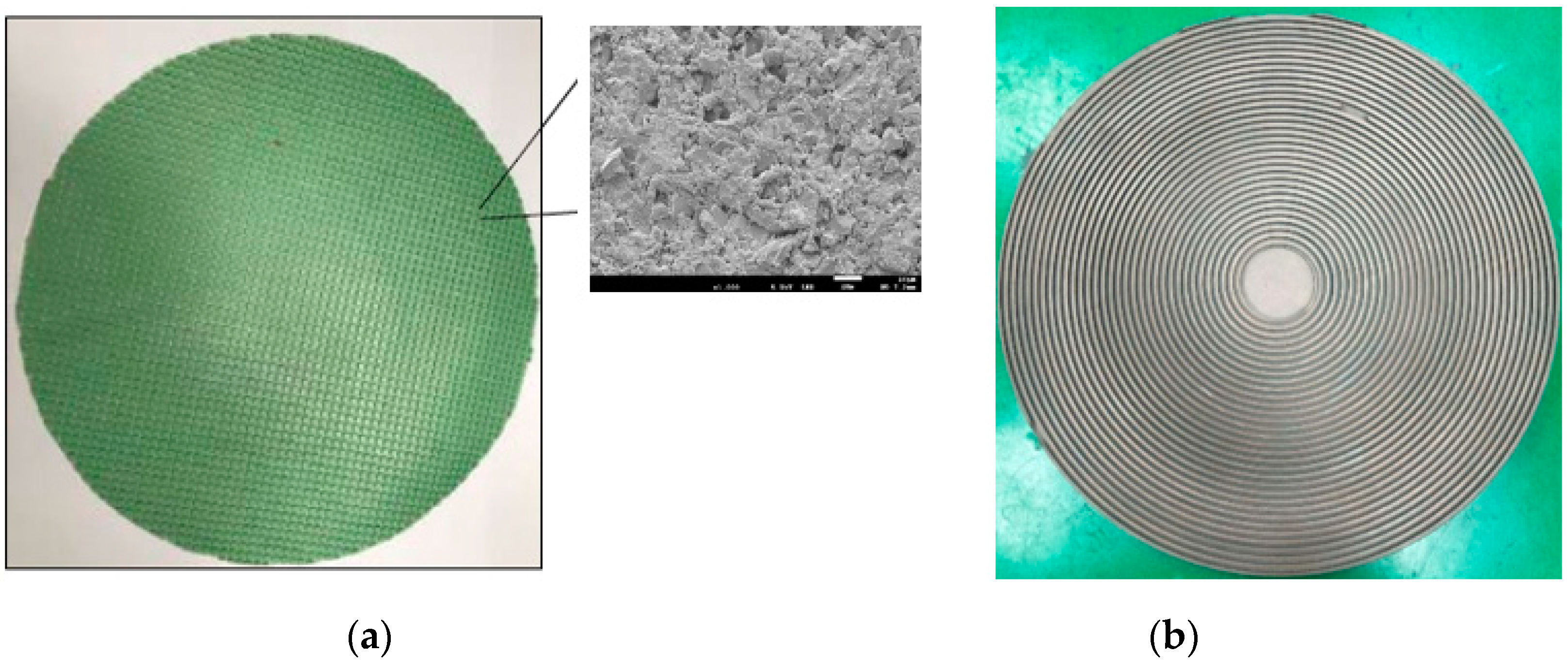
Figure 7.
(a) The polishing system; (b) the polishing pad; (c) SEM image of the pad surface (top) and diamond dresser (bottom).
Figure 7.
(a) The polishing system; (b) the polishing pad; (c) SEM image of the pad surface (top) and diamond dresser (bottom).

Figure 8.
Wear rate of diamond grinding plates.

Figure 9.
Silicon carbide material removal rate: (a) material removal rate; (b) grinding ratio.
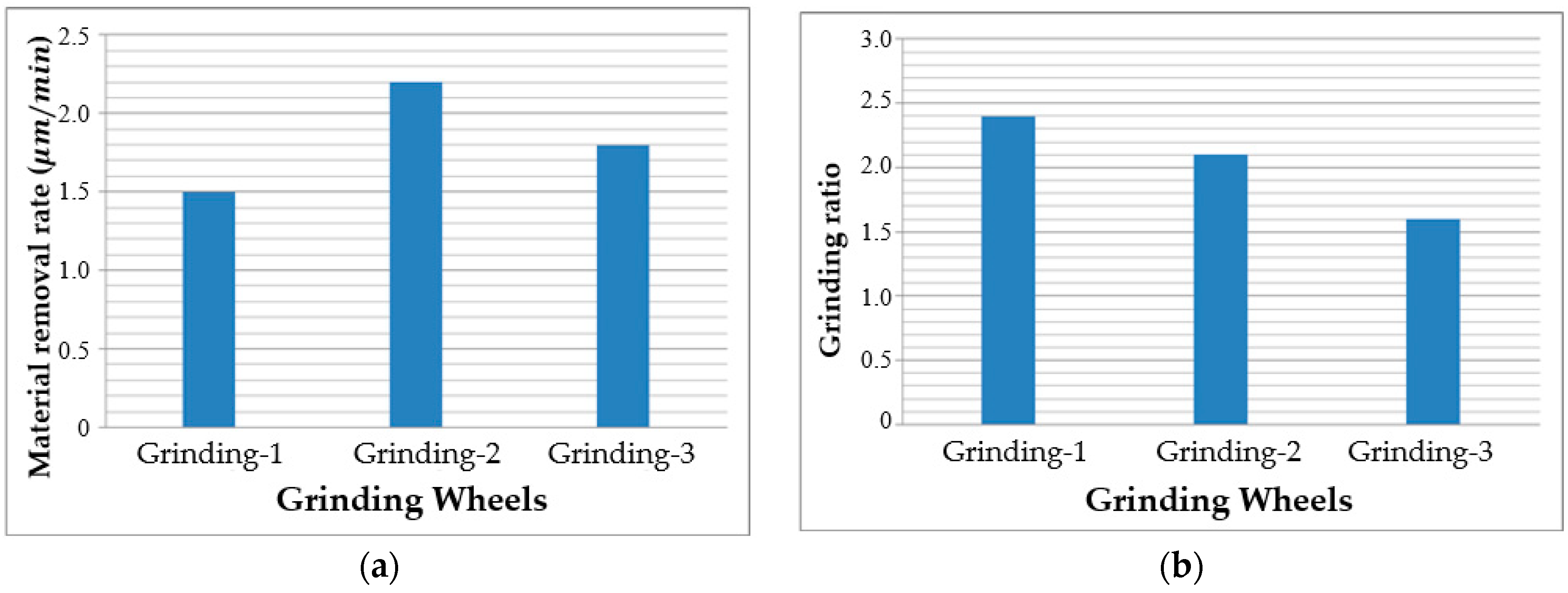
Figure 10.
SEM images of diamond grinding pad surfaces: (a) Grinding-1; (b) Grinding-2; (c) Grinding-3 (bar is 1 µm).
Figure 10.
SEM images of diamond grinding pad surfaces: (a) Grinding-1; (b) Grinding-2; (c) Grinding-3 (bar is 1 µm).
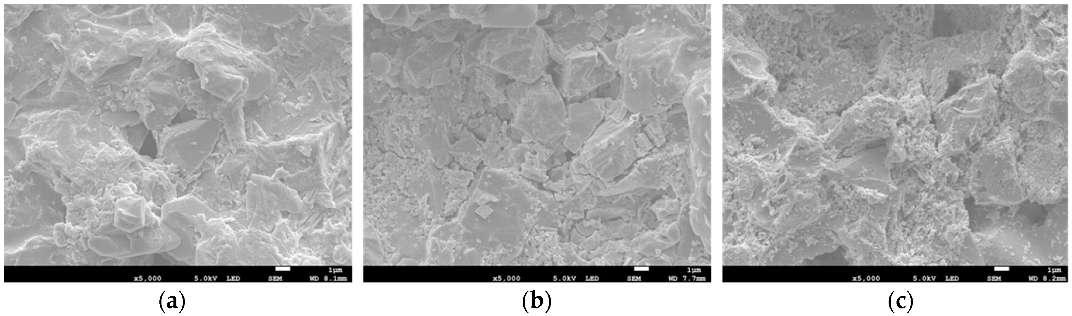
Figure 11.
Surface roughness of ground SiC wafers: (a) Sa and (b) Sz.
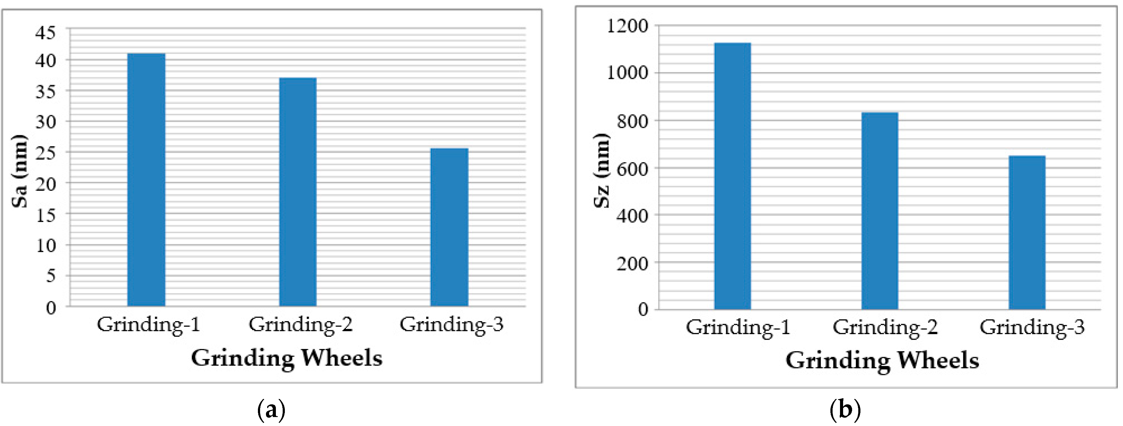
Figure 12.
Zygo images of SiC surface: (a) Grinding-1; (b) Grinding-2; (c) Grinding-3.

Figure 13.
Silicon carbide material removal rate of lapping processes.
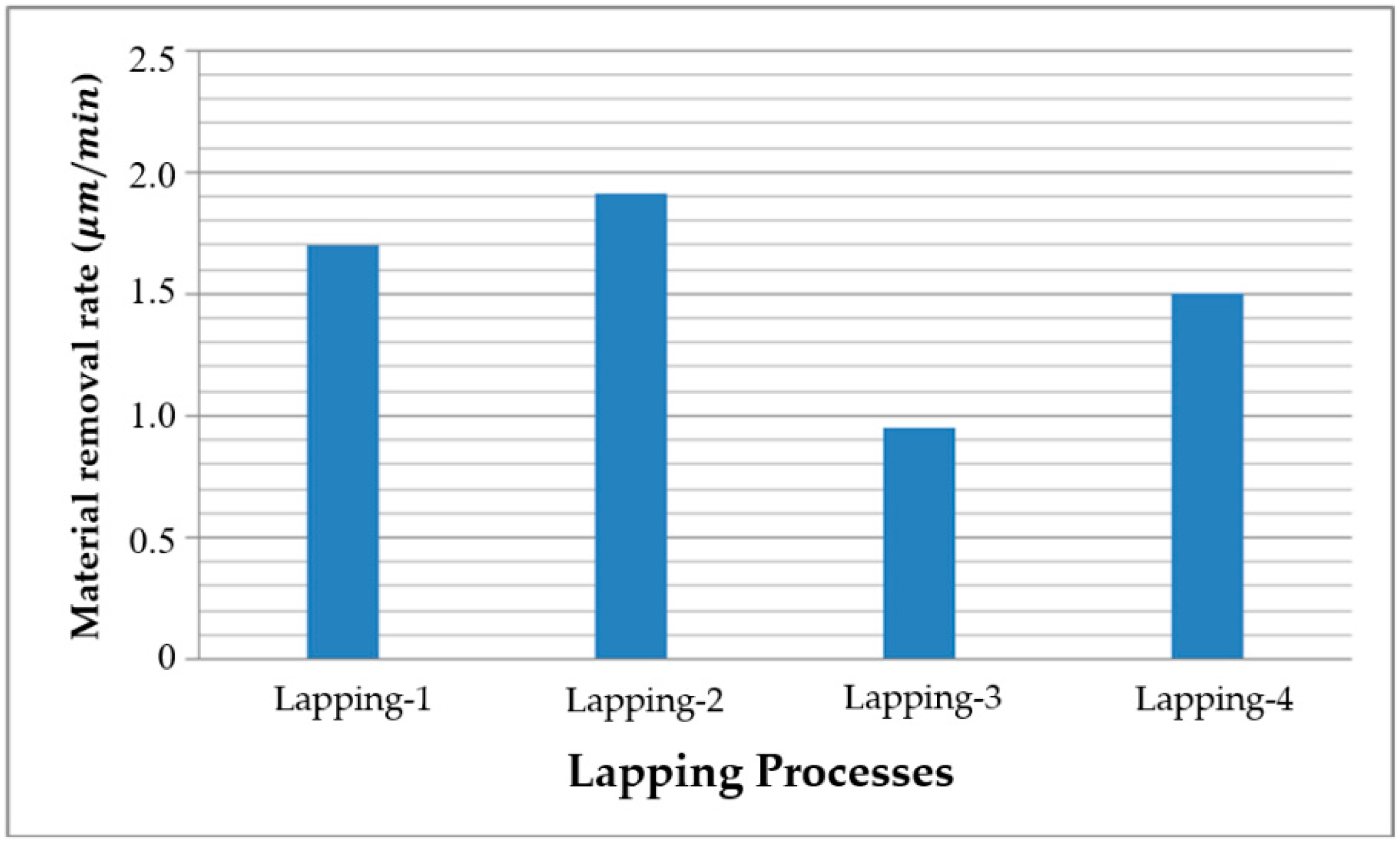
Figure 14.
Surface roughness of grinding SiC wafers: (a) Sa; (b) Sz.
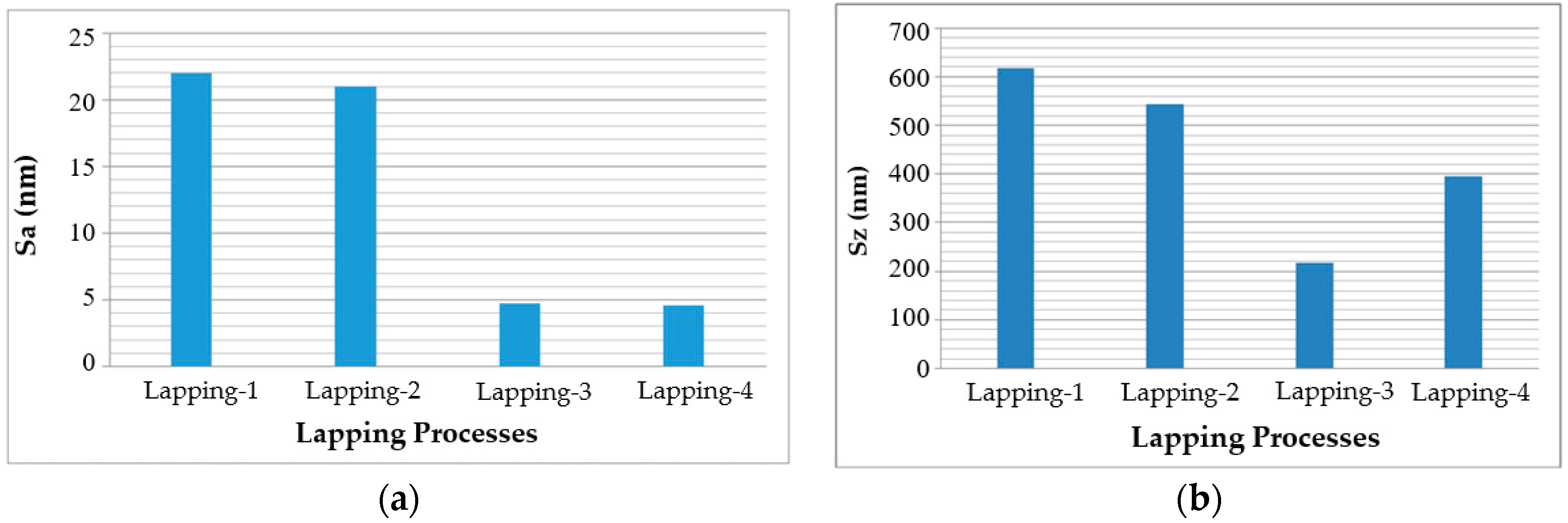
Figure 15.
Zygo images of the SiC surface: (a) Lapping-1; (b) Lapping-2; (c) Lapping-3; (d) Lapping-4.
Figure 15.
Zygo images of the SiC surface: (a) Lapping-1; (b) Lapping-2; (c) Lapping-3; (d) Lapping-4.
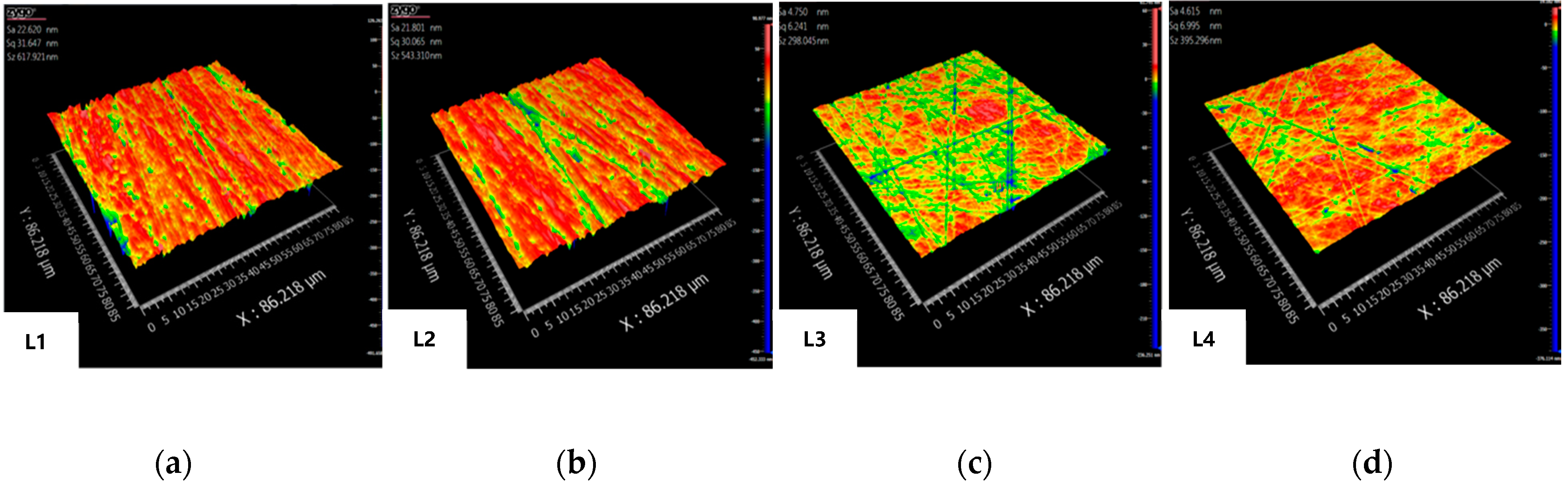
Figure 16.
Surface morphology of the copper plate surface: (a) original; (b) after lapping; (c) after dressing.
Figure 16.
Surface morphology of the copper plate surface: (a) original; (b) after lapping; (c) after dressing.

Figure 17.
Surface morphology of the self-made plate surface: (a) original; (b) after lapping; (c) after dressing.
Figure 17.
Surface morphology of the self-made plate surface: (a) original; (b) after lapping; (c) after dressing.
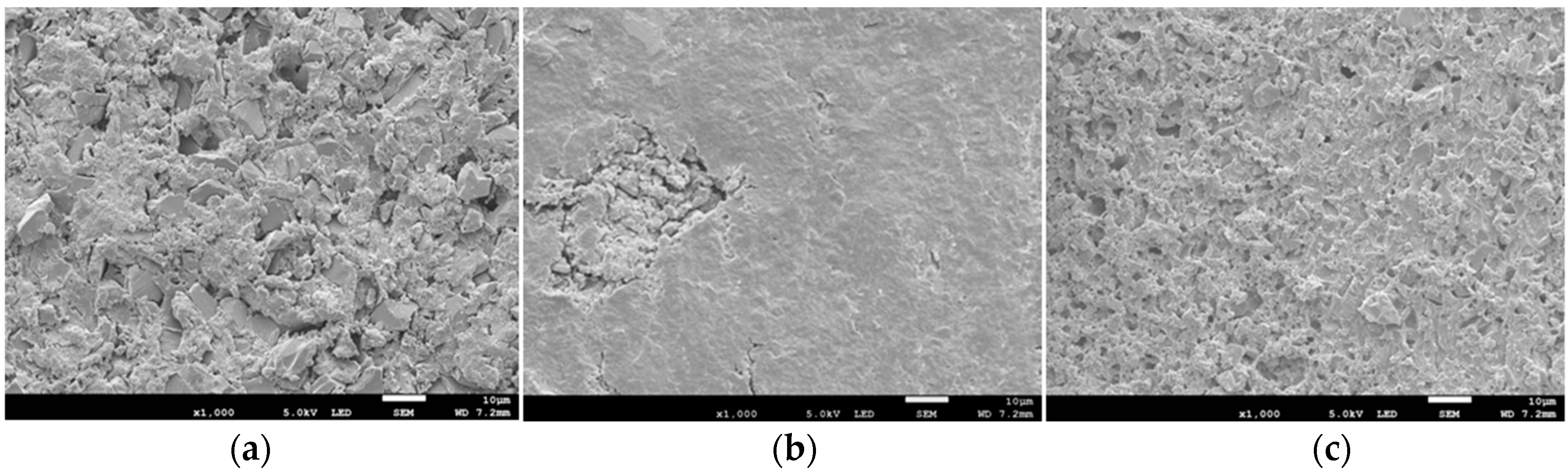
Figure 18.
Schematics of the contact interaction (a) between the copper plate and the SiC wafer and (b) between the self-made lapping plate and the SiC wafer.
Figure 18.
Schematics of the contact interaction (a) between the copper plate and the SiC wafer and (b) between the self-made lapping plate and the SiC wafer.

Table 1.
The three types of diamond pads.
| Grinding | Diamond | SiO2 | Al2O3 | SiC | Ceramic Binder | Temperature |
|---|---|---|---|---|---|---|
| 1 | 50 v% | - | - | 10.79 v% | 39.21 v% | 700 °C |
| 2 | 50 v% | - | - | 10.79 v% | 39.21 v% | 700 °C |
| 3 | 16.67 v% | 16.67 v% | 16.67 v% | 10.79 v% | 39.21 v% | 700 °C |
Table 2.
The four types of lapping processes used.
| Lapping | |
|---|---|
| 1 | Copper plate + industrial diamond slurry |
| 2 | Copper plate + self-modified diamond (SMD) slurry |
| 3 | Self-made resin diamond plate + pure water |
| 4 | Self-made resin diamond plate + self-modified diamond (SMD) slurry |
Publisher’s Note: MDPI stays neutral with regard to jurisdictional claims in published maps and institutional affiliations. |
© 2021 by the authors. Licensee MDPI, Basel, Switzerland. This article is an open access article distributed under the terms and conditions of the Creative Commons Attribution (CC BY) license (http://creativecommons.org/licenses/by/4.0/).
Share and Cite
MDPI and ACS Style
Tsai, M.-Y.; Li, K.-Y.; Ji, S.-Y. Novel Abrasive-Impregnated Pads and Diamond Plates for the Grinding and Lapping of Single-Crystal Silicon Carbide Wafers. Appl. Sci. 2021, 11, 1783. https://doi.org/10.3390/app11041783
AMA Style
Tsai M-Y, Li K-Y, Ji S-Y. Novel Abrasive-Impregnated Pads and Diamond Plates for the Grinding and Lapping of Single-Crystal Silicon Carbide Wafers. Applied Sciences. 2021; 11(4):1783. https://doi.org/10.3390/app11041783
Chicago/Turabian StyleTsai, Ming-Yi, Kun-Ying Li, and Sun-Yu Ji. 2021. "Novel Abrasive-Impregnated Pads and Diamond Plates for the Grinding and Lapping of Single-Crystal Silicon Carbide Wafers" Applied Sciences 11, no. 4: 1783. https://doi.org/10.3390/app11041783
Note that from the first issue of 2016, this journal uses article numbers instead of page numbers. See further details here.