A Gap Waveguide-Based Compact Rectangular Waveguide to a Packaged Microstrip Inline Transition


1
Antenna Group, Public University of Navarra, 31006 Pamplona, Spain
2
Institute of Smart Cities, Public University of Navarra, 31006 Pamplona, Spain
*
Author to whom correspondence should be addressed.
Appl. Sci. 2020, 10(14), 4979; https://doi.org/10.3390/app10144979
Submission received: 25 June 2020
/
Revised: 15 July 2020
/
Accepted: 17 July 2020
/
Published: 20 July 2020
(This article belongs to the Special Issue Millimeter-wave and Terahertz Applications of Metamaterials)
Abstract
:In this paper two different simple to design and easy to manufacturing transitions from a microstrip to rectangular waveguide based on ridge and groove gap waveguides are studied. The first one is based on a combination of a groove and ridge gap waveguide. In this case, the microstrip substrate occupies the whole bottom metallic housing block, namely, the transition and the gap between the bed of nails and the lid; therefore, it does not require any substrate shaping. Nevertheless, the transition needs to replace groove waveguide by ridge gap waveguide sections to avoid higher-order mode excitation. In the second approach, based on only a groove gap waveguide, the substrate is shaped to be only in the microstrip section, that is, outside the bed of nails area. This leads to a simplification of the design procedure. Prototypes of both transitions have been characterized, showing good agreement with the simulations taking into account the manufacturing tolerances. Performance comparable to the state-of-the-art in this frequency band has been achieved.
1. Introduction
Gap waveguide technology-based components have been getting a lot of attention in the last few years [1,2]. These components are based on the so-called bed of nails [3], a periodic structure composed by metallic pins covered by a metal lid. This bed of nails creates an artificial magnetic conductor (AMC) or high impedance surface (HIS) that prevents electromagnetic wave propagation in a certain frequency region [4]. Such a property has been successfully used for microwave and millimeter wave circuit packaging, avoiding resonances which could degrade their performance [5,6,7].
Taking this structure as the baseline, waveguides can be created if an air channel is formed in between two bed of nail sections, which behave as high impedance surfaces and forbid electromagnetic wave propagation in any direction other than the air channel formed in between them. This channel can have different forms, depending on its height, its section and the presence of a dielectric substrate, leading to different types of waveguides [8,9,10]. Based on these waveguides a variety of components [11,12,13,14,15] have been created. In addition, the reduction of cross-talk effects allows for improving the performances of different components such as grid amplifiers [16]. Finally, gap waveguide technology has been proposed as an alternative solution for antenna array feeding networks [17,18].
The properties of these waveguides have been explored, and found to be similar to those of an equivalent standard rectangular or ridge metal waveguide. However, there is a fundamental advantage in terms of fabrication that makes these waveguides of great interest, since they do not require electrical contact between the pins and the lid that covers them. In addition to the rectangular or ridge waveguide behavior, the gap waveguide can perform similarly to a microstrip line. That is the case for the ridge gap waveguide (RGW), which overcomes the significant transmission losses that dielectric substrates introduce in planar transmission lines such as microstrips, in the millimeter wave range and above.
Therefore, for these waveguides, manufacturing and assembly of sub-millimeter wave components can be largely simplified, since, in particular, gap waveguide components allow H-plane cutting. This property has been explored in the aforementioned components and in other packaging applications. In this field, they have deserved attention for the design of transitions from planar to waveguide technology for frequencies higher than 60 GHz, which can be of interest for integration of MMIC and waveguide-based components [19,20,21]. The use of gap waveguides has been shown to simplify assembly and allows working wide dielectric substrates.
In this paper, two simplified inline transitions from microstrip to standard rectangular waveguides employing gap waveguide technology are presented. This type of transition has been long studied and some relevant examples can be found in the literature [22,23,24,25,26]. In this case the design method and configurations have some similarities with that presented in [27,28], since all of them are based on Chebyshev transformers. However, in this case the transition design benefits from the use of of gap waveguide sections. First, the need for good electrical contact between upper and bottom parts in [27] is alleviated. Moreover, the intricate shapes required in [28] are avoided in this case. Therefore, manufacturing and assembly are simplified, leading to cost reduction with respect to previous designs.
Note also that, as a difference to [28], in this work the gap waveguide sections are just used to implement the Chebyshev sections and include the dielectric substrate as a part of the bed of nails, which allows working with wide substrates, without requiring any shaping. However, the design procedure complicates things, since there are limitations in the design caused by the higher-order modes than can propagate in some of the dielectric-filled Chebyshev transformer steps. These limitations are overcome in the second configuration, where the substrate does not fill any step of the Chebyshev transformer; instead all the groove gap waveguide sections work in the monomode regime. Finally, we shown that the microstrip taper can be substituted by a ridge waveguide section. In all cases the proposed solutions present simpler assembly when compared with other alternatives.
This paper is organized as follows. Firstly, Section 2 describes the proposed transition and the theoretical methods for their design. Since these transitions make use of a partially-dielectric-filled groove gap waveguide, the analysis of this type of waveguide is presented in Section 3. Thereafter, in Section 4 the transition design procedure is explained. Then, Section 5 shows the simulation results of the proposed structures. The manufacturing procedure and the experimental validation are presented in Section 6. Finally, conclusions are drawn in Section 7.
2. Transition Concepts
Two different transitions are studied in this work. They are based on different gap waveguide configurations and described in the following sections.
2.1. Dielectric-Filled Ridge and Groove Gap Waveguide Based Transition
The first structure consists of a Chebyshev transformer implemented using ridge and groove gap waveguide sections, which are partially filled by the microstrip line dielectric substrate. This transformer matches the standard rectangular waveguide to the ridge groove gap waveguide. To complete the transition to microstrip line, a tapered microstrip line section connects the ridge gap waveguide section to the microstrip line. The 3D perspective view of the structure is presented in Figure 1a. The rectangular waveguide would directly connect to the first section of the Chebyshev transformer.
This transition has the advantage of being suitable for wide substrates, since the substrate, which fills partially the gap between the bed of nails and the lid, is included in the design of the ridge and groove gap waveguide sections.
2.2. Ridge and Groove Gap Waveguide-Based Transition
The second proposed configuration is shown in Figure 1b. Formally, it is simpler than the previous transition, since it consists just of a Chebyshev transformer, implemented in groove gap waveguide sections. It presents two advantages with respect to the previous configuration: no microstrip line taper is required, and since the microstrip substrate does not enter the bed of nails area, the design of the Chebyshev transformer is simplified.
3. Groove Gap Waveguide Characteristics
The cores of both transitions are groove gap waveguide (GGW) sections. The propagation characteristics of this type of gap waveguide have been studied, and its performance has been found to be similar to that of an equivalent rectangular waveguide, whose width is narrower than the width of the GGW channel [29,30]. However, in the first proposed transition we are dealing with partially filled GGW. Therefore, the propagation characteristics of this dielectric-filled GGW have been analyzed.
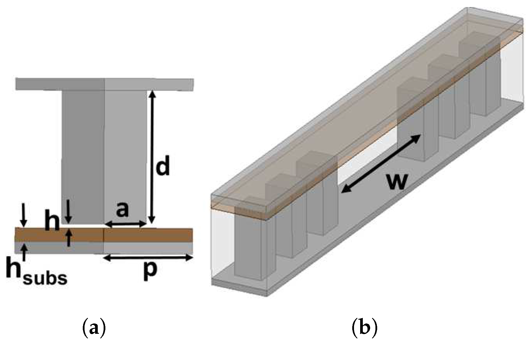
In addition, in order to facilitate the use of this transition with wide microstrip substrates, the gap between the pins and the lid was partially filled with a dielectric substrate, specifically, a 100 μm thick slab of Rogers CuClad 233 ( and ) with 17 μm copper cladding. The structure of the pins can be seen in Figure 2a and the optimized dimensions are compiled in Table 1. These dimensions provide a bandgap between 25 and 125 GHz.
For this analysis, the height of the GGW, including the dielectric substrate thickness, was the same as that of the equivalent rectangular waveguide. Since the design was done in the W-band (75–110 GHz), it corresponds to the height of the WR10 waveguide, i.e., 1.27 mm.
Using this bed of nails, waveguides with different width, w in Figure 2b, have been analyzed, and their propagation constant, β, has been obtained. These results are shown in Figure 3, where they are compared with the propagation constant of a WR10 rectangular waveguide.
It can be observed that the propagation constant for all widths is similar at high frequencies. However, the behavior at low frequencies turns out to be quite different. The cut-off frequency of the GGW is higher than the cut-off frequency of the standard rectangular waveguide for the same propagation channel width. This effect is ascribed to the smaller electrical dimensions of the GGW when compared with the rectangular waveguide. In addition, larger dispersion was present in the GGW [30]. In this case, the most similar behavior in terms of propagation constant with the WR10 waveguide corresponds to GGW width w = 2.65 mm.
4. Transition Design
For the design of the Chebyshev transformer, which matches the standard rectangular waveguide to the first section of the GGW, the procedure presented in [27] has been followed. The impedances of the different transformer sections were calculated by the standard formulation [31]. The order of the transition, 5, has been calculated to reach 20 dB return loss in the full W-band. The impedance of the groove gap waveguide sections was adjusted by changing their height according to the waveguide electric impedance formula [32].
where is the free-space impedance and is the effective dielectric constant of the partially filled gap waveguide section. The waveguide width, a, corresponds to the width of the equivalent rectangular waveguide that provides the same propagation constant as the gap waveguide. Finally, b is the height of each waveguide section, and its value is used to control the impedance of each section. Since depends also on b, an iterative process is followed until the height that provides the desired impedance is obtained.
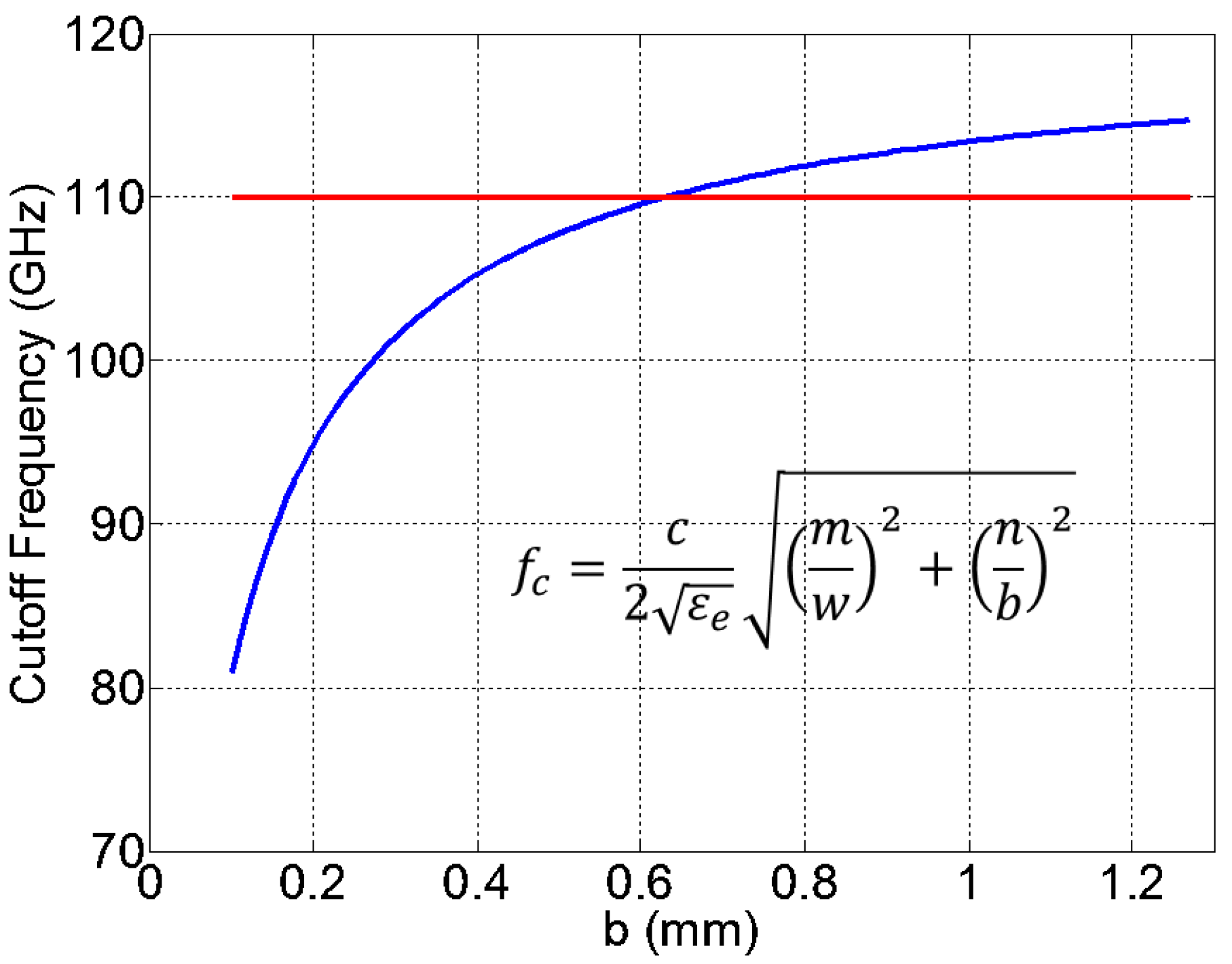
For the first transition it must be taken into account that the GGW is partially filled with the dielectric substrate. Therefore, the effective dielectric constant, , changes with different GGW heights. As a consequence, if changes, the cutoff frequency () of the second order mode of this waveguide, i.e., the , also does: the smaller the GGW height, the higher the , and consequently, the lower the cut-off frequency. The main implication of this behavior is that for small waveguide heights the effective dielectric constant will be close to and the second order mode of the partially filled GGW can be in propagation in the W-band. Therefore, an analysis of the cut-off frequency of the second order mode of the GGW, , versus the waveguide height (b) was carried out. The results are shown in Figure 4 for a constant width GGW, with mm [33]. It can be observed that for waveguide heights lower than 0.6 mm, is so high that the second mode propagates within the W-band; therefore, those GGW sections whose height, , allows propagation of this second order mode are substituted by ridge gap waveguide sections in order to achieve the required impedance without the presence of higher-order modes.
This is not a problem for the second transition, in which the dielectric substrate does not fill any of the steps of the Chebyshev transformer. In this case we have one metal step that connects the microstrip and the groove gap waveguide transformer calculated by the standard formulation. The metal step is calculated as a dielectric-filled ridge gap waveguide in order to have the same impedance as the microstrip line. That way, the function of the ridge metal step is just to ensure the connection between the microstrip and the Chebyshev transformer based on groove gap waveguide.
Finally, the second part of the transition is a microstrip taper that matches the 50 Ω microstrip line to the impedance of the dielectric-filled ridge gap waveguide (DFRGW) [34] for the first design. For the second case there is no need for a microstrip taper and the 50 Ω microstrip line is directly connected to a ridge waveguide with the same width (and impedance) as the microstrip line.
5. Simulation Results
The procedure above has been applied to a microstrip to standard rectangular waveguide transition working at W-band. The dimensions obtained are compiled in Table 2 and Table 3 for the first and second models, respectively. A perspective view of the Chebyshev transformer and a top view of the microstrip to ridge gap waveguide transition are shown in Figure 5 and Figure 6.
First, both parts of the transition were simulated separately using the 3D full-wave simulator Ansys High Frequency Structure Simulator (HFSS), based on the finite element method. The performance of the first transition is shown in Figure 7. Since a back-to-back configuration was used for experimental validation, a comparison between the performances of single and back-to-back configurations is presented in the same figure. In the case of the back-to-back configuration, both transitions were connected by a 5.18 mm long microstrip line.
For the single transition the return loss is better than 20 dB for almost the whole bandwidth (77–107.9 GHz). The mean return loss is 23.9 dB, and in the whole W-band bandwidth, it is below 15.74 dB. For the back-to-back configuration the performance slightly degrades: the return loss is better than 19 dB within the 75–108.3 GHz bandwidth. This slight degradation of the return loss performance, compared to the single transition, is ascribed to the reflections due to the non-perfect matching at both ports. On the other hand, the single transition presents insertion loss below 0.6 dB, with mean value 0.3 dB. The back-to-back transition has a maximum insertion loss of 1.3 dB and a 0.6 dB mean value. This insertion loss increment is mainly caused by the losses associated with the 5.18 mm microstrip line in between both transitions. However, in both cases the insertion loss is below 1 dB and the return loss is better than 19 dB.
For the second transition model, the comparison of the predicted response of single and back-to-back configurations is shown in Figure 8. The single transition performs return loss higher than 15 dB for the whole W-band and better than 20 dB from 80 GHz to 107.3 GHz. The mean value is 26.68 dB. The insertion losses are lower than 0.5 dB and its mean value is 0.27 dB. On the other hand, the back-to-back transition performs return loss higher than 10 dB for the whole band and better than 15 dB from 78 GHz to 107 GHz.
6. Experimental Validation
As mentioned above, a back-to-back transition has been designed for experimental validation. The fabrication process included milling for the metallic component and photolithography for the microstrip line. The aluminum block was realized by CNC machining. The lid and the pins were manufactured in separated metal blocks. For the first transition model, six screws guaranteed the connection between top and bottom parts and four dowel pins the proper alignment. Besides, there were four dowel pins and two screws for substrate alignment and positioning, respectively. The dimensions of the whole block were 13.65 mm in length and 25.05 mm in width.
For the second transition, four screws were used for the connection between bottom and top parts. Four dowel pins guaranteed the metallic block alignment and four other pins the substrate alignment. Two screws held the substrate to the block. The dimensions of the whole block were 13.14 mm length and 32 mm width.
For both cases the microstrip taper transition was built in 100 μm thick Rogers CuClad 233 substrate ( and ) with 17 μm copper cladding using a standard photolithography process at the Public University of Navarra’s facilities. Figure 9a shows a top view of the microstrip line mounted on the bottom metallic block and of the upper metallic block, which contained the bed of nails. Figure 9b is a perspective view of the metallic blocks for the second model and of the microstrip line printed on the substrate.
For both cases the experimental setup was the same. The whole structure was assembled and connected between VDI W-band VNA extenders, and connected to an Agilent PNA-X E3861 vector network analyzer, as can be seen in Figure 10.
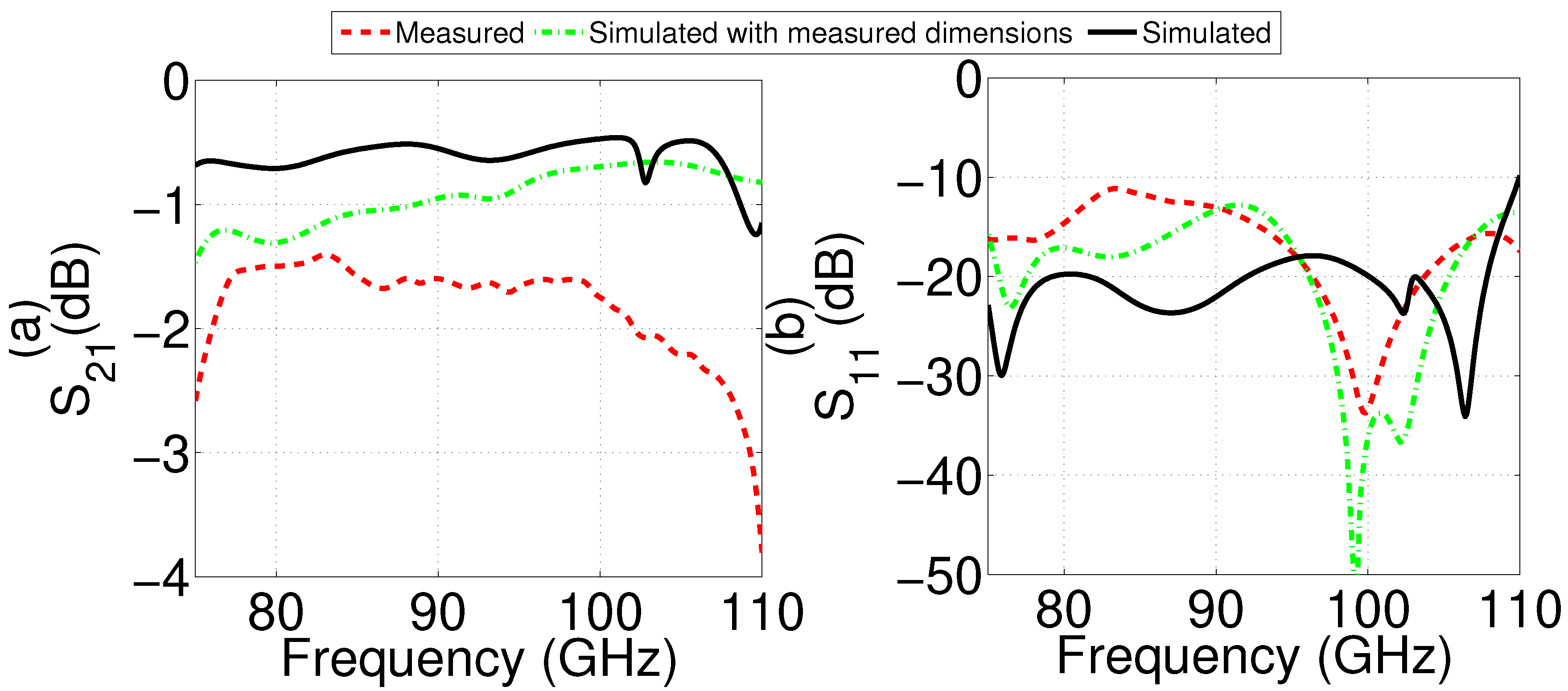
The results of the measurement and its comparison with the predicted response of the back-to-back configuration are shown in Figure 11. The simulation of the back-to-back transition was realized using the dimensions of the fabricated components, shown in Table 2. Due to the manufacturing errors, the behavior degraded with respect to that presented in Figure 7. In the lower part of the working bandwidth, both insertion and return losses were slightly higher than in the predicted response, whilst in the upper part of the band the increase of insertion losses was higher, although there was not a significant increase in the return loss. This discrepancy in the measurements was ascribed to the assembly tolerances and to a higher than the nominal value of the loss tangent.
Nevertheless, the simulated insertion loss was lower than 1 dB and the mean value was 0.6 dB. However, the mean measured insertion loss increased 1.3 dB with a maximum of 3.8 dB at high frequencies. This effect can be ascribed to larger losses in the substrate. Regarding return losses, these were higher than 14.8 dB with a 19.8 dB mean value, whereas the measured mean value was 17.2 dB and the minimum was 12.15 dB.
For the second prototype, the results of the measurement and its comparison with the predicted response of the back-to-back configuration are shown in Figure 12. The experimental results are also compared with the simulation of the back-to-back transition using the dimension of the fabricated component and a misalignment of 150 μm in the perpendicular to the waveguide axis direction, Table 3.
It can be observed that the insertion losses were higher than the simulated ones. In the predicted performance of the transition the mean insertion loss was 0.35 dB while in the measured results it increased until 3.97 dB. The return loss also showed degradation; in this case the mean value was 10.48 dB instead of 19.75 dB. In this case the degradation can be associated with the losses ascribed to the substrate, whose value may be different to the nominal one since the loss tangent tends to increase with frequency. A possibility to reduce the insertion losses could be the use of a substrate with a lower loss tangent, e.g., a cyclic olefin copolymer (COC)-based substrate. This type of substrate has been successfully used in submillimeter wave applications [35,36]. However, for this demonstrative work a standard substrate was selected. Furthermore, another degradation factor could be the manufacturing and assembly errors. In particular, alignment between the microstrip and ridge waveguides has been found to have large impact on the transition response, as is shown in Figure 13. Misalignments larger than 100 μm increase the return loss more than 2 dB. Additional losses can also be ascribed to a high roughness of the aluminium block, which directly increases the losses in the waveguide sections.
Summarizing, we can observe that the behavior of the return loss is quite similar to the predicted evaluation of the prototype once the fabrication tolerances have been taken into account for both cases.
7. Conclusions
Two simple inline microstrip to standard rectangular waveguide transitions based on a Chebyshev transformer implemented in gap waveguide technology have been studied in this paper. Both designs are suitable for analytical design, which simplifies the whole procedure. Besides, the configurations used in this work avoid any kind of soldering and losses caused in the H-plane cuts of the waveguide, thanks to band-gap created by the bed of nails which surrounds the gap waveguide. Therefore, as contact between the upper and bottom part is not required, the fabrication tolerances can be relaxed. This, plus the fact that intricate shapes are avoided, reduces their cost with respect to other configurations [20,26,27].
In the first configuration, since the substrate covers the whole bottom metallic block, problems associated to substrate cutting with a specific shape are avoided, which simplifies manufacturing. However, the first steps of the transition must be replaced for ridge gap waveguide in order to avoid higher-order mode propagation, which adds complexity to the design process. Evenly, thanks to the microstrip line taper which ensures good contact with the ridge gap waveguide, the transition is more tolerant to misalignment.
The second transition suppresses the microstrip taper transition, but at the expense of using a narrow ridge gap waveguide section which makes the circuit less tolerant to misalignments. However, in this case the substrate does not cover the whole gap between the bed of nails and the lid. This way, any possibility of higher-order mode propagation is avoided and the design procedure is simplified. Finally, in order to prove these concepts, W-band back-to-back transitions were validated and a comparison with the state-of-the-art is shown in Table 4 featuring similar performances. These transitions are, therefore, a good alternative to other designs.
Author Contributions
Investigation: J.M.P.-E., A.E.T.-G., R.G. and I.E.; writing—original draft: J.M.P.-E.; writing—review and editing: I.E. All authors have read and agreed to the published version of the manuscript.
Funding
This research was funded by the Spanish Ministry of Economy and Competitiveness, project numbers TEC2013-47753-C3-1-R, TEC2016-76997-C3-1-R and PID2019-109984RB-C43.
Conflicts of Interest
The authors declare no conflict of interest.
Abbreviations
The following abbreviations are used in this manuscript:
| AMC | Artificial Magnetic Conductor |
| DFRGW | Dielectric-Filled Ridge Gap Waveguide |
| GGW | Groove Gap Waveguide |
| HFSS | High Frequency Structure Simulator |
| HIS | High Impedance Surface |
| MMIC | Monolithic microwave and integrated circuits |
| RGW | Ridge Gap Waveguide |
| RW | Rectangular Waveguide |
References
- Zaman, A.U.; Kildal, P.S. Gap Waveguides. In Handbook of Antenna Technologies; Chen, Z., Ed.; Springer: Singapore, 2015. [Google Scholar]
- Rajo-Iglesias, E.; Ferrando-Rocher, M.; Zaman, A.U. Gap Waveguide Technology for Millimeter-Wave Antenna Systems. IEEE Commun. Mag. 2018, 56, 14–20. [Google Scholar] [CrossRef] [Green Version]
- Rajo-Iglesias, E.; Kildal, P.S. Numerical studies of bandwidth of parallel-plate cut-off realised by a bed of nails, corrugations and mushroom-type electromagnetic bandgap for use in gap waveguides. IET Microw. Antennas Propag. 2011, 5, 282–289. [Google Scholar] [CrossRef] [Green Version]
- Rajo-Iglesias, E.; Zaman, A.U.; Kildal, P.S. Parallel plate cavity mode suppression in microstrip circuit packages using a lid of nails. IEEE Microw. Wirel. Compon. Lett. 2010, 20, 31–33. [Google Scholar] [CrossRef]
- Rajo-Iglesias, E.; Pucci, E.; Kishk, A.A.; Kildal, P.S. Suppression of parallel plate modes in low frequency microstrip circuit packages using lid of printed zigzag wires. IEEE Microw. Wirel. Compon. Lett. 2013, 23, 359–361. [Google Scholar] [CrossRef] [Green Version]
- Zaman, A.U.; Alexanderson, M.; Vukusic, T.; Kildal, P.S. Gap waveguide PMC packaging for improved isolation of circuit components in high-frequency microwave modules. IEEE Trans. Compon. Packag. Manuf. Technol. 2014, 4, 16–25. [Google Scholar] [CrossRef] [Green Version]
- Rebollo, A.; Gonzalo, R.; Ederra, I. Optimization of a Pin Surface as a Solution to Suppress Cavity Modes in a Packaged W-band Microstrip Receiver. IEEE Trans. Compon. Packag. Manuf. Technol. 2014, 4, 975–982. [Google Scholar] [CrossRef]
- Kildal, P.S.; Alfonso, E.; Valero-Nogueira, A.; Rajo-Iglesias, E. Local metamaterial-based waveguides in gaps between parallel metal plates. IEEE Antennas Wirel. Propag. Lett. 2009, 8, 84–87. [Google Scholar] [CrossRef]
- Kildal, P.S.; Zaman, A.U.; Rajo-Iglesias, E.; Alfonso, E.; Valero-Nogueira, A. Design and experimental verification of ridge gap waveguide in bed of nails for parallel-plate mode suppression. IET Microw. Antennas Propag. 2011, 5, 262–270. [Google Scholar] [CrossRef]
- Vosoogh, A.; Zaman, A.U.; Vassilev, V.; Yang, J. Zero-Gap Waveguide: A Parallel Plate Waveguide with Flexible Mechanical Assembly for mm-Wave Antenna Applications. IEEE Trans. Compon. Packag. Manuf. Technol. 2018, 8, 2052. [Google Scholar] [CrossRef]
- Farahbakhsh, A.; Zarifi, D.; Zaman, A.U. 60-GHz Groove Gap Waveguide Based Wideband H-Plane Power Dividers and Transitions: For Use in High-Gain Slot Array Antenna. IEEE Trans. Microw. Theory Technol. 2017, 65, 4111–4121. [Google Scholar] [CrossRef] [Green Version]
- Ali, M.M.M.; Sebak, A. Compact Printed Ridge Gap Waveguide Crossover for Future 5G Wireless Communication System. IEEE Microw. Wirel. Compon. Lett. 2018, 28, 549–551. [Google Scholar] [CrossRef]
- Chieh, J.C.S. A Substrate-Less Microwave Power-Combining Module Utilizing Ridge Gap Waveguide. IEEE Microw. Wirel. Compon. Lett. 2018, 28, 972–974. [Google Scholar] [CrossRef]
- Horestani, A.K.; Shahabadi, M. Balanced Filter With Wideband Common-Mode Suppression in Groove Gap Waveguide Technology. IEEE Microw. Wirel. Compon. Lett. 2018, 28, 132–134. [Google Scholar] [CrossRef]
- Vosoogh, A.; Sorkherizi, M.S.; Zaman, A.U.; Yang, J.; Kishk, A.A. An Integrated Ka-Band Diplexer-Antenna Array Module Based on Gap Waveguide Technology With Simple Mechanical Assembly and No Electrical Contact Requirements. IEEE Trans. Microw. Theory Tech. 2018, 66, 962–972. [Google Scholar] [CrossRef]
- Aljarosha, A.; Smolders, A.B.; Ivashina, M.; Maaskant, R. Toward wide-band low-loss gap-waveguide- integrated grid amplifiers. In Proceedings of the 2017 International Symposium on Antennas and Propagation (ISAP), Phuket, Thailand, 30 October–2 November 2017; pp. 1–2. [Google Scholar]
- Shi, Y.; Feng, W.; Wang, H.; Che, W.; Xue, Q.; Wang, J.; Cao, B. Novel W-band LTCC Transition from Microstrip Line to Ridge Gap Waveguide and Its Application in 77/79 GHz Antenna Array. IEEE Trans. Antennas Propag. 2019, 67, 915–924. [Google Scholar] [CrossRef]
- Cao, J.; Wang, H.; Mou, S.; Quan, S.; Ye, Z. W-Band High-Gain Circularly Polarized Aperture-Coupled Magneto-Electric Dipole Antenna Array With Gap Waveguide Feed Network. IEEE Antennas Wirel. Propag. Lett. 2017, 6, 2155–2158. [Google Scholar] [CrossRef]
- Zaman, A.U.; Vukusic, T.; Alexanderson, M.; Kildal, P.S. Design of a Simple Transition From Microstrip to Ridge Gap Waveguide Suited for MMIC and Antenna Integration. IEEE Antennas Wirel. Propag. Lett. 2013, 12, 1558–1561. [Google Scholar] [CrossRef]
- Shi, Y.; Zhang, J.; Zeng, S.; Zhou, M. Novel W-band Millimeter Wave Transition From Microstrip Line to Groove Gap Waveguide for MMIC Integration and Antenna Application. IEEE Trans. Antennas Propag. 2018, 66, 3172–3176. [Google Scholar] [CrossRef]
- Nandi, U.; Zaman, A.U.; Vosoogh, A.; Yang, J. Millimeter wave contactless microstrip-gap waveguide transition suitable for integration of RF MMIC with gap waveguide array antenna. In Proceedings of the 2017 11th European Conference on Antennas and Propagation (EUCAP), Paris, France, 19–24 March 2017; pp. 1682–1684. [Google Scholar]
- Hassan, E.; Berggren, M.; Scheiner, B.; Michler, F.; Weigel, R.; Lurz, F. Design of Planar Microstrip-to- Waveguide Transitions Using Topology Optimization. In Proceedings of the IEEE Radio and Wireless Symposium (RWS), Orlando, FL, USA, 20–23 January 2019; pp. 1–3. [Google Scholar]
- Li, J.; Li, L.; Qiao, Y.; Chen, J.; Chen, J.; Zhang, A. Full Ka band waveguide-to-microstrip inline transition design. J. Infrared Millim. Terahertz Waves 2018, 39, 714–722. [Google Scholar] [CrossRef]
- Algaba-Brazález, A.; Flygare, J.; Yang, J.; Vassilev, V.; Baquero-Escudero, M.; Kildal, P.S. Design of F-Band Transition From Microstrip to Ridge Gap Waveguide Including Monte Carlo Assembly Tolerance Analysis. IEEE Trans. Microw. Theory Tech. 2016, 64, 1245–1254. [Google Scholar] [CrossRef] [Green Version]
- Zhang, Y.; Ruiz-Cruz, J.A.; Zaki, K.A.; Piloto, A.J. A Waveguide to Microstrip Inline Transition With Very Simple Modular Assembly. IEEE Microw. Wirel. Compon. Lett. 2010, 20, 480–482. [Google Scholar] [CrossRef]
- Rebollo, A.; Gonzalo, R.; Ederra, I. An Inline Microstrip-to-Waveguide Transition Operating in the Full W-Band. J. Infrared Millim. Terahertz Waves 2015, 36, 734–744. [Google Scholar] [CrossRef]
- Pérez-Escudero, J.M.; Torres-García, A.E.; Gonzalo, R.; Ederra, I. A Simplified Design Inline Microstrip-to- Waveguide Transition. Electronics 2018, 7, 215. [Google Scholar] [CrossRef] [Green Version]
- Pérez-Escudero, J.M.; Torres-García, A.E.; Gonzalo, R.; Ederra, I. A Chebyshev Transformer Based Microstrip to Groove Gap Waveguide Inline Transition for MMIC Packaging. IEEE Trans Compon. Packag. Manuf. Technol. 2019, 9, 1595–1602. [Google Scholar] [CrossRef] [Green Version]
- Rajo-Iglesias, E.; Kildal, P.S. Groove gap waveguide: A rectangular waveguide between contactless metal plates enabled by parallel-plate cut-off. In Proceedings of the Fourth European Conference on Antennas and Propagation, Barcelona, Spain, 12–16 April 2010; pp. 1–4. [Google Scholar]
- Berenguer, A.; Fusco, V.; Zelenchuk, D.E.; Sánchez-Escuderos, D.; Baquero-Escudero, M.; Boria-Esbert, V.E. Propagation characteristics of groove gap waveguide below and above cutoff. IEEE Trans. Microw. Theory Technol. 2016, 4, 27–36. [Google Scholar] [CrossRef] [Green Version]
- Orfanidis, S.; Electromagnetic Waves and Antennas. ECE Department Rutgers University. Available online: https://www.ece.rutgers.edu/~orfanidi/ewa/ (accessed on 4 August 2017).
- Eshrah, I.A.; Kishk, A.A.; Yakovlev, A.B.; Glisson, A.W. Rectangular waveguide with dielectric-filled corrugations supporting backward waves. IEEE Trans. Microw. Theory Technol. 2005, 53, 3298–3304. [Google Scholar] [CrossRef]
- Harrington, R.F. Time Harmonic Electromagnetic Field; Wiley-IEEE Press: Hoboken, NJ, USA, 2001. [Google Scholar]
- Pozar, D.M. Microwave Engineering; John Wiley & Sons: Hoboken, NJ, USA, 2011; pp. 256–261. [Google Scholar]
- Maestrojuan, I.; Palacios, I.; Ederra, I.; Gonzalo, R. Use of COC substrates for millimeter-wave devices. Microw. Opt. Technol. Lett. 2015, 57, 371–377. [Google Scholar] [CrossRef]
- Peytavit, J.; Donche, C.; Lepilliet, S.; Ducournau, G.; Lampin, J.-F. Thin film transmission lines using cyclic olefin copolymer for millimeter-wave and terahertz integrated circuits. Electron. Lett. 2011, 47, 453–454. [Google Scholar] [CrossRef]
Figure 1.
3D view of the proposed microstrip to rectangular waveguide transitions. (a) Dielectric-filled ridge and groove gap waveguide-based transition (RW-RGW-GGW-μstrip). (b) Groove gap waveguide-based transition (RW-GGW-μstrip).
Figure 1.
3D view of the proposed microstrip to rectangular waveguide transitions. (a) Dielectric-filled ridge and groove gap waveguide-based transition (RW-RGW-GGW-μstrip). (b) Groove gap waveguide-based transition (RW-GGW-μstrip).

Figure 2.
Perspective view of unit cells of: (a) metallic pin and (b) groove gap waveguide partially filled with Rogers CuClad substrate.
Figure 2.
Perspective view of unit cells of: (a) metallic pin and (b) groove gap waveguide partially filled with Rogers CuClad substrate.

Figure 3.
Comparison of the propagation constant of width (w) groove gap waveguides and a WR10 standard rectangular waveguide. The gray areas correspond to the limits of the bandgap of the bed of nails.
Figure 3.
Comparison of the propagation constant of width (w) groove gap waveguides and a WR10 standard rectangular waveguide. The gray areas correspond to the limits of the bandgap of the bed of nails.

Figure 4.
Cut-off frequency of the second mode of the GGW for channel heights. (Inset) Cut-off frequency expression, where c is the speed of light and m and n are the indexes of the mode, (2,0) in this case. The red line represents the upper limit of the W-band.
Figure 4.
Cut-off frequency of the second mode of the GGW for channel heights. (Inset) Cut-off frequency expression, where c is the speed of light and m and n are the indexes of the mode, (2,0) in this case. The red line represents the upper limit of the W-band.

Figure 5.
Microstrip to standard rectangular transition: (a) perspective view of the Chebyshev transformer split in half for the first model and (b) for the second model.
Figure 5.
Microstrip to standard rectangular transition: (a) perspective view of the Chebyshev transformer split in half for the first model and (b) for the second model.

Figure 6.
Microstrip to standard rectangular transition: (a) top view of the taper from a microstrip to a dielectric ridge gap waveguide; (b) top view of the microstrip to ridge gap waveguide transition.
Figure 6.
Microstrip to standard rectangular transition: (a) top view of the taper from a microstrip to a dielectric ridge gap waveguide; (b) top view of the microstrip to ridge gap waveguide transition.

Figure 7.
Predicted response of the first model of microstrip to standard WR-10 single (solid line) and back-to-back transitions (dashed line).
Figure 7.
Predicted response of the first model of microstrip to standard WR-10 single (solid line) and back-to-back transitions (dashed line).

Figure 8.
Simulation of the scattering parameters for the microstrip to standard WR-10 single (solid line) and back-to-back transitions (dashed line), second prototype: (left) insertion loss and (right) return loss.
Figure 8.
Simulation of the scattering parameters for the microstrip to standard WR-10 single (solid line) and back-to-back transitions (dashed line), second prototype: (left) insertion loss and (right) return loss.

Figure 9.
Photographs of the fabricated structures: (a) top view of the first transition model aluminum block and microstrip circuit and (b) perspective view of the second transition model aluminum block and microstrip circuit.
Figure 9.
Photographs of the fabricated structures: (a) top view of the first transition model aluminum block and microstrip circuit and (b) perspective view of the second transition model aluminum block and microstrip circuit.

Figure 10.
Photograph of the assembled structures connected to the VDI W-band VNA extenders for the first (a) and second models (b).
Figure 10.
Photograph of the assembled structures connected to the VDI W-band VNA extenders for the first (a) and second models (b).

Figure 11.
Comparison between predicted response (black solid line) and simulated transition taking into account the fabricated value (green dashed-point line) and measured (red dashed line) back-to-back configuration of the first transition model prototype (Figure 1a): (left) insertion loss and (right) return loss.

Figure 12.
Comparison between predicted response (black solid line), simulated transition taking into account the fabricated value (green dashed-point line) with 150 μm of misalignment and measured (red dashed line) back-to-back configuration of the second transition model prototype (Figure 1b): (left) insertion loss and (right) return loss.

Figure 13.
Analysis of tolerances for a misalignment of the microstrip on the x-direction in second prototype (Figure 1b): (left) insertion loss and (right) return loss.
Figure 13.
Analysis of tolerances for a misalignment of the microstrip on the x-direction in second prototype (Figure 1b): (left) insertion loss and (right) return loss.


Table 1.
Dimensions of the bed of nails used in the two proposed transitions.
| Parameter | Description | Value (μm) Transition (a) | Value (μm) Transition (b) |
|---|---|---|---|
| a | pin size | 500 | 600 |
| d | pin height | 1120 | 1190 |
| h | air gap | 34 | 80 |
| p | period | 1050 | 1240 |
| substrate thickness | 100 | 100 |
Table 2.
Dimensions of the first transition model; see Figure 1a for reference. All dimensions in m.
Table 2.
Dimensions of the first transition model; see Figure 1a for reference. All dimensions in m.
| Parameter | Design Value | Fabricated Value |
|---|---|---|
| w | 2650 | 2590 |
| 1200 | 1130 | |
| 115 | 116 | |
| 130 | 116 | |
| 377 | 361 | |
| 852 | 909 | |
| 1200 | 1212 | |
| 400 | 470 | |
| 550 | 470 | |
| 673 | 685 | |
| 705 | 683 | |
| 726 | 697 | |
| 1500 | 1467 | |
| 1300 | 1256 |
Table 3.
Dimensions of the second transition; see Figure 1 for reference. All dimensions in m.
Table 3.
Dimensions of the second transition; see Figure 1 for reference. All dimensions in m.
| Parameter | Design | Fabricated |
|---|---|---|
| 300 | 317 | |
| 325 | 256 | |
| 115 | 158 | |
| 325 | 378 | |
| 700 | 758 | |
| 975 | 957 | |
| 1195 | 1053 | |
| 1270 | 1253 | |
| 500 | 430 | |
| 820 | 826 | |
| 820 | 830 | |
| 820 | 870 | |
| 840 | 807 | |
| 840 | 907 | |
| w | 2650 | 2590 |
| b | 1270 | 1280 |
© 2020 by the authors. Licensee MDPI, Basel, Switzerland. This article is an open access article distributed under the terms and conditions of the Creative Commons Attribution (CC BY) license (http://creativecommons.org/licenses/by/4.0/).
Share and Cite
MDPI and ACS Style
Pérez-Escudero, J.M.; Torres-García, A.E.; Gonzalo, R.; Ederra, I. A Gap Waveguide-Based Compact Rectangular Waveguide to a Packaged Microstrip Inline Transition. Appl. Sci. 2020, 10, 4979. https://doi.org/10.3390/app10144979
AMA Style
Pérez-Escudero JM, Torres-García AE, Gonzalo R, Ederra I. A Gap Waveguide-Based Compact Rectangular Waveguide to a Packaged Microstrip Inline Transition. Applied Sciences. 2020; 10(14):4979. https://doi.org/10.3390/app10144979
Chicago/Turabian StylePérez-Escudero, José M., Alicia E. Torres-García, Ramón Gonzalo, and Iñigo Ederra. 2020. "A Gap Waveguide-Based Compact Rectangular Waveguide to a Packaged Microstrip Inline Transition" Applied Sciences 10, no. 14: 4979. https://doi.org/10.3390/app10144979
Note that from the first issue of 2016, this journal uses article numbers instead of page numbers. See further details here.