Theoretical Study of Electromagnetic Interference Shielding of 2D MXenes Films

1
Optoelectronics and Energy & Collaborative Innovation Center of Suzhou Nano Science and Technology, College of Physics, Soochow University, Suzhou 215006, China
2
Key Laboratory of Modern Optical Technologies of Ministry of Education & Key Lab of Advanced Optical Manufacturing Technologies of Jiangsu Province, Suzhou 215006, China
*
Authors to whom correspondence should be addressed.
Metals 2018, 8(8), 652; https://doi.org/10.3390/met8080652
Submission received: 9 July 2018
/
Revised: 11 August 2018
/
Accepted: 13 August 2018
/
Published: 20 August 2018
(This article belongs to the Special Issue Metallic Films: From Nanofabrication and Nanostructuration to Characterizations and Applications)
Abstract
:The advance of research on 2D transition metal carbides, carbonitrides, and nitrides (collectively known as MXenes) has progressed rapidly since the introduction of Ti3C2 in 2011. Nowadays the number of MXene synthesized in lab has reached more than 20, while there are currently about 20 theoretically predicted structures. In this study, we calculate the electromagnetic interference shielding effectiveness of a series of MXene films in theory and find that the results are in good agreement with the measured data. From this, we can use this method to calculate electromagnetic properties of all kinds of 2D material films which are similar to Mxenes.
1. Introduction
Two-dimensional (2D) materials have unusual electronic, mechanical, and optical properties, which have led to their extensive study in the past decade for diverse applications [1,2,3,4,5,6]. For example, the first 2D material, graphene [7], has received a high level of attention. Currently, Mxenes, a family of 2D material with good flexibility and high conductivity, have been comprehensively investigated, which can provide electromagnetic interference shielding with minimal thickness [8]. Electromagnetic interference (EMI) comes from electronic devices that transmit, distribute, or use electrical energy, which has inferior impacts on device performance and the surrounding environment [9,10,11,12]. So it is important to judge whether a material has a good electromagnetic shielding performance. An effective EMI shielding material must meet two conditions: One is to reduce undesirable emissions and the other one is to preserve the component from straying external signals. The reflection of radiation for EMI shielding is the primary function by using charge carriers, which directly related to the electromagnetic properties. As a result, the first factor of shielding materials is electrically conductive. However, electrical conductivity is not the only element affecting the EMI shielding. Absorption of EM radiation is the second element for EMI shielding, the principle of which is that the material’s electric and magnetic dipoles interact with the radiation.
Different MXenes are expressed with chemical formula Mn+1XnTx, where M is transition metal, X is carbon and/or nitrogen, and T represents surface termination. Among them, Ti3C2Tx is the most commonly studied MXene, because of its excellent electrical conductivity. In particular, the EMI shielding capabilities of several Ti3C2Tx films and the polymer composites (Ti3C2Tx-SA) have been experimentally examined at microwave frequencies and have been reported to be the highest synthetic materials with comparable thickness [8]. In this study, we present a theoretical calculation for conductive MXene films to shield microwave to understand the measurement reported in Ref. [8]. Note that the difference of result between experimental measurement and theoretical calculation is very small.
2. Theoretical Calculation
The electromagnetic interference shielding effectiveness (EMI SE) is a way to measure a material’s ability to block electromagnetic waves. When an electromagnetic radiation is incident on a shielding device, the energy of the electromagnetic radiation will be reflected, absorbed, and transmitted. The sum of the three components must be 1. The contributions of the total EMI SE (EMI SET) are derived from reflection, absorption and multiple internal reflections. The total SET can be written as:
where SER denotes the reflection contribution and SEA is the absorption contribution with multiple internal reflections (SEM) included implicitly. The two quantities can be expressed in terms of reflectance (R) and transmittance (T) as:
Inserting Equations (2) and (3) into Equation (1), we can obtain the EMI SE:
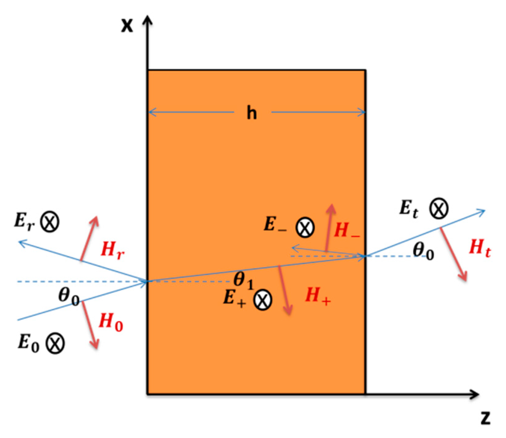
Transmission and reflection coefficients of a conductive thin film, schematically illustrated in Figure 1, can be solved through matching boundary conditions and utilizing Fresnel formula, as following:
where z0 is the vacuum wave impedance, z1 is the impedance of the film, is the incident angle, is the refracting angle in the film, is the vacuum wave vector, k is the wave vector of the film, h is the thickness of the film, E0 is the electric field of the incident wave, Er is the electric field of the reflection wave, Et is the electric field of the transmission wave, E+ and E− are the electric fields of electromagnetic wave inside the film, accounting for internal reflections. From Equations (5)–(8), we obtain the obliquely-incident TE-wave (transverse electric wave) transmittance and reflectance of a conductive thin film (nonmagnetic material) in vacuum:
where , , , , and . In the above equations, is the relative permittivity of the film, is the conductivity of the film, is the angular frequency, and c is the speed of light in vacuum. The theoretical model has considered the factor of multiple internal reflections, so the Equations (9) and (10) apply to the structure of the film in Reference [8].
Applying Equation (9) to Equation (4) and assuming the normal incidence of plane wave, we can obtain: [13]
where n is complex refraction of the film and k is the complex wave vector which is related with n (k = k1 + ik2 = n/c). Then, Equation (11) can be divided explicitly into the following three terms:
Specific to the conductive films, where the measuring frequency is very low (σ/(ωε0) ≫ 1), we can use two relations of εr ≈ iσ/(ωε0) and k1 = k2 to simplify Equations (12) and (13). Finally, we can obtain the approximate expressions as following:
where h is the film thickness in the unit of centimeter, f is the measuring frequency in the unit of MHz and is the electrical conductivity in the unit of S/cm. The sum of SEA and SER is the widely-used Simon formalism (seeing Supplementary Text of Ref. [8]). As such, there are two differences between our theory and Simon formalism. First, the multiple internal reflection contribution, SEM, is omitted in Simon formalism, but we consider it. Second, Simon formalism applies only to the normally-incident case of plane wave, but our theory contains the incident angle, and can also be used to calculate the incident case of waveguide mode where the propagating constant of waveguide mode gives rise to the incident angle.
Results and Discussion
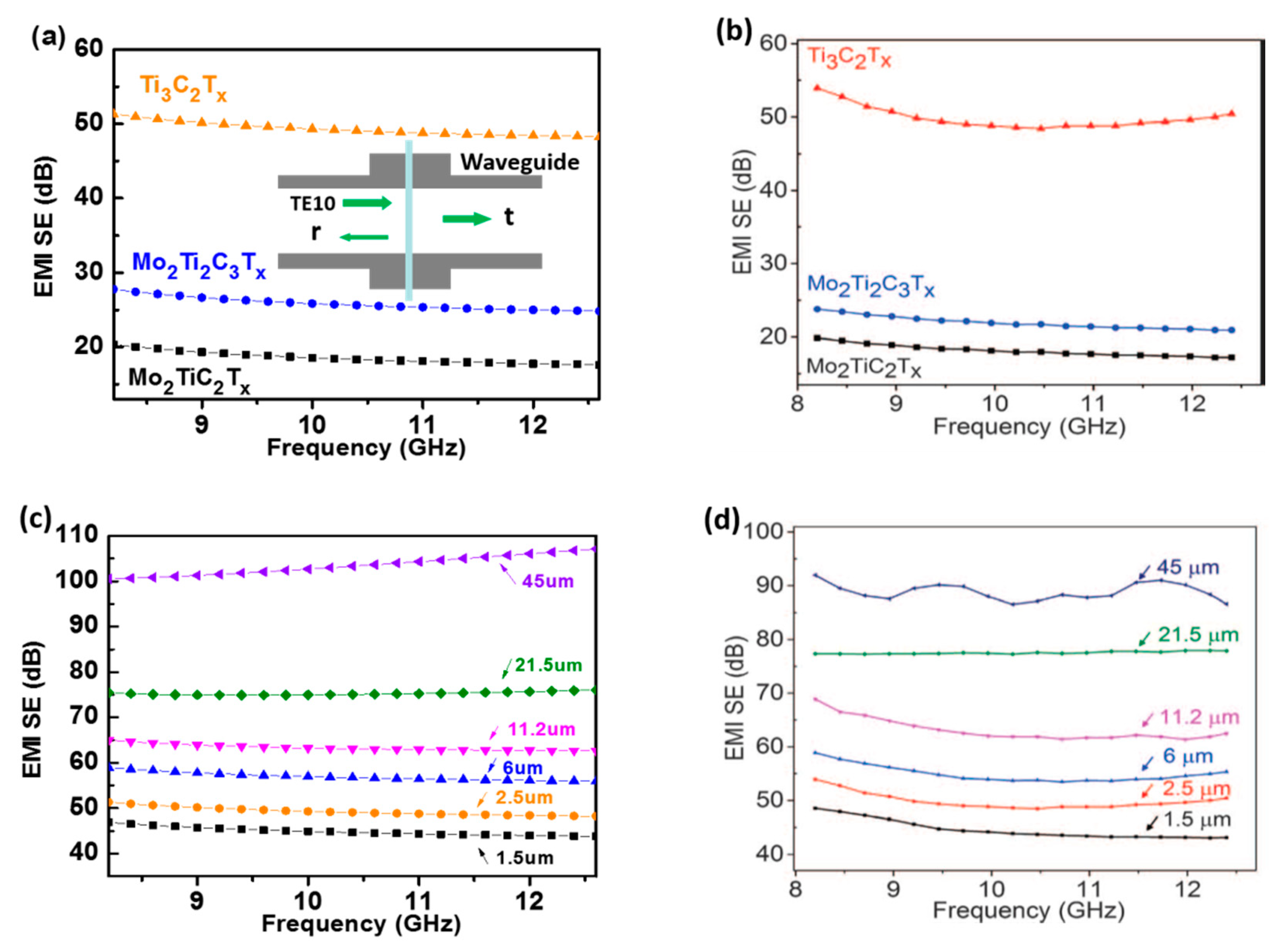
The MXenes were chemically synthesized and delaminated, and they were prepared into freestanding films via vacuum-assisted filtration [8]. According to the reported measurements in Ref. [8], the shielding properties of the MXenes are characterized within the TE10 waveguide, as illustrated schematically by the inset in Figure 2a. A microwave network analyzer (Agilent ENA5071C) was used to record reflection and transmission coefficients, r (S11) and t (S21), of port 1 and port 2 which were connected with two identical coax-to-waveguide adapters (X-band, WR-90, 8.2–12.4 GHz). Before measuring the sample, the two ports for the waveguide system were calibrated with X-band standards (seeing Materials and Methods of Ref. [8]). Then, the MXenes and composite samples with areas larger than the cross-section of the waveguide were loaded into the measuring system. The microwave TE10 mode, which was launched from the WR-90 adapter of port 1, propagated toward the sample, and the transmission and reflection spectra were obtained. Finally, the EM shielding can be calculated from Equation (4), where the transmittance T = |t|2.
In our calculation, is defined using the propagating constant β of the TE10 mode as , where a is the broadside length of the rectangular waveguide. The calculated results are shown in Figure 2a,c, which are seen to agree well with the measured data in Ref. [8]. The difference of 45 μm thick Ti3C2Tx films between theoretical calculation (Figure 2c) and experimental measurement (Figure 2d) arises from the network analyzer, because the dynamic range of the network analyzer in experiment is 80 dB.
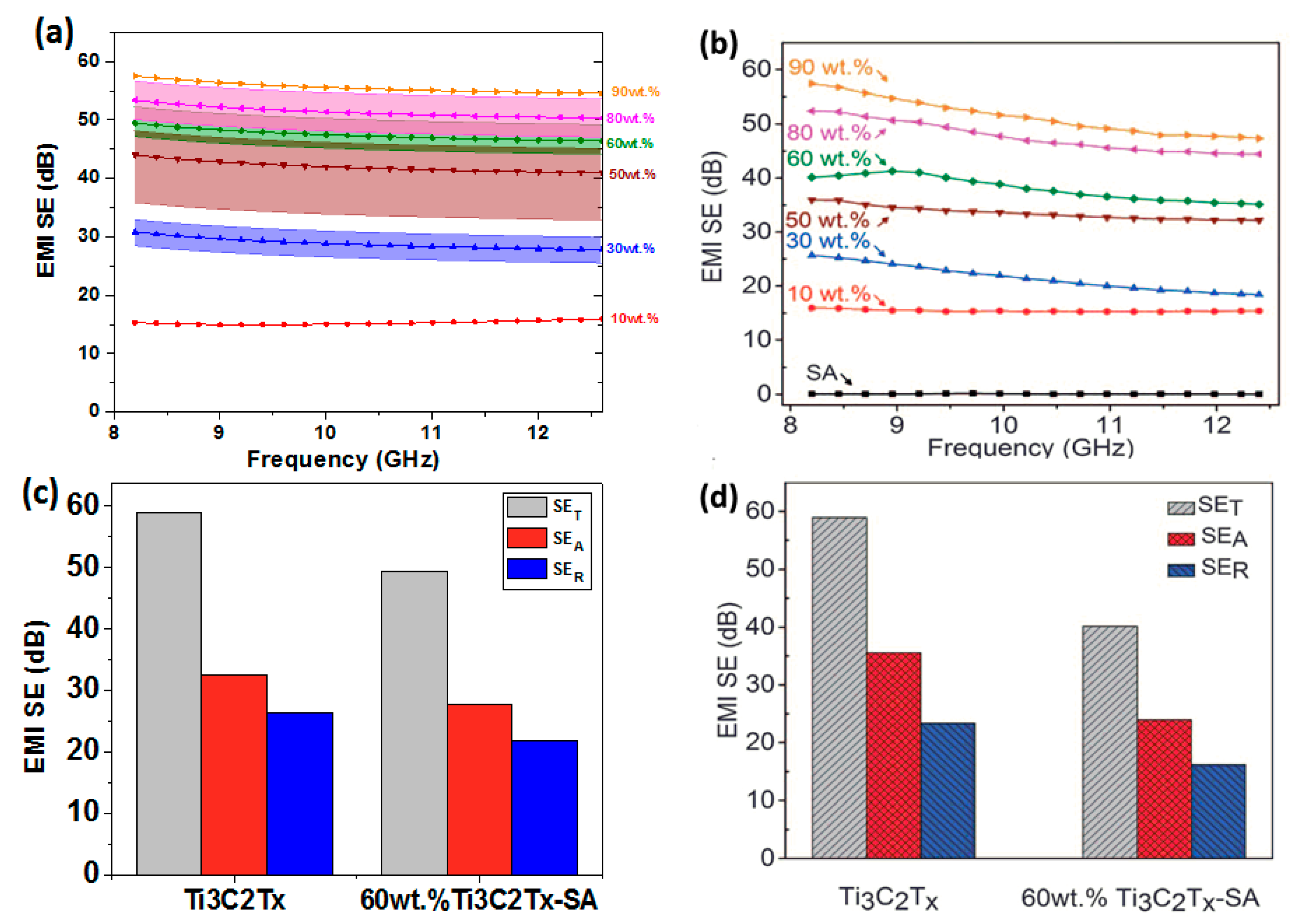
In order to improve tensile strength while maintaining good conductivity, Reference [8] fabricated and measured the conductive composite consisting of Ti3C2Tx and Sodium Alginate (SA, a naturally occurring polymer). In Figure 3, we display the calculation of EMI shielding effectiveness of Ti3C2Tx-SA composites with different Ti3C2Tx concentrations, whose thickness and conductivity are adopted from Reference [8]. It is seen that the agreement at the case of high conductivity (i.e., the 90 wt.% concentration) is good, whereas the agreement at the cases of medium conductivity (e.g., the concentrations of 30 wt.%~60 wt.%) is moderate. Note that there are noticeable variations of electrical conductivity measured for the intermediate concentrations, which is plotted in Reference [8]. Taking the uncertainty of electrical conductivity into account, the agreement is improved, as depicted by the color ribbons in Figure 3. For the 10 wt.% case, the conductivity is at least three order of magnitude lower than other concentration cases, which is likely due to being around the percolation threshold. Fitting these conductivities into a power-law relation, , where v denotes the volume concentration of the conducting filler, vc is the critical volume concentration at the percolation threshold and s is the exponent beyond the threshold [14], will find vc close to the 10 wt.% concentration. With such low conductivity, the description of is not applicable, and the real part of should be changed much larger than 1. This is because a large amount of microscopic gaps/contacts between the conducing fillers inside the composite around the percolation will lead to a strong capacitive effect (i.e., polarization effect) and consequently a large real part of permittivity [15,16]. Therefore, for the 10 wt.% concentration, real part of has been modified to be 5000 to best match our calculation and the measurement.
In particular cases, where the thickness of the film is very small (nk0h 1 with the refractive index ) and the measurement frequency is very low (), we can use the two approximation conditions, i.e., and to simplify Equations (9) and (10). Then, we can obtain the approximate expressions as following:
In the above equations, Rs is the sheet resistance with the definition .
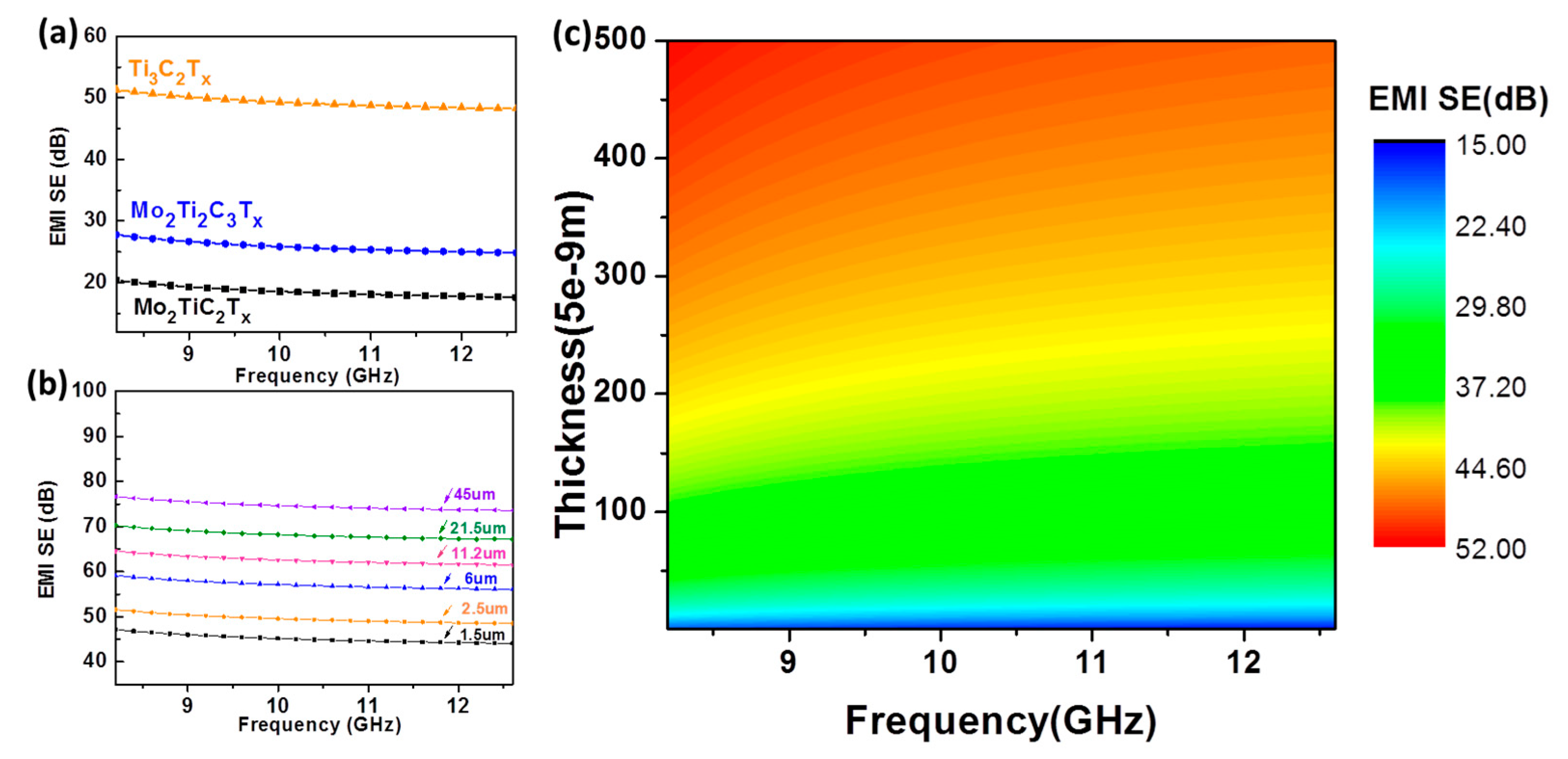
We find that the calculation results of EMI shielding effectiveness of three MXene films with Equations (11) and (12) are nearly same as Equations (9) and (10), when comparing Figure 2a and Figure 4a. This is because the case of the three MXene films is satisfied with the approximate conditions. But with the increase of the thickness of Ti3C2Tx films, we find that the calculation results in Figure 2c and Figure 4b are very different when the thickness is greater than 11.2 um. In case of thick films, the aforementioned approximate condition, nk0h 1, is no longer valid, which can be justified through comparing the film thickness and the skin depth. On the other hand, in the opposite case where the MXene films range nm-scaled thickness, our equations are applicable for calculating the shielding effectiveness. For example, assuming the Ti3C2Tx conductivity is thickness-independent down to 50 nm, Equation (11) is used to predict the shielding effectiveness and the calculated results are displayed in Figure 4c, which shows the map of EMI SE as a function of frequency and thickness. It is noticed that the Ti3C2Tx film needs to only be ~50 nm thick to meet the SE requirement of 20 dB.
Since the superior EMI shielding of MXenes was reported, there are the intense investigations towards the direction [17,18]. Most used the Simon formalism to explain their experimental results. However, SE from the calculation based on Simon formalism consistently underestimates the experimental values due to neglecting the term of SEM in Equation (14), and is not rigorous to the waveguide measurement, as aforementioned. Our formulas add all contributing factors to the shielding effectiveness, and give a more accurate prediction to the shielding measurement with the waveguide system.
3. Conclusions
In conclusion, the electromagnetic properties of emerging 2D materials can be modeled and calculated by the Fresnel formula of a generic conductive thin film. The comparison between the calculation and the measurement is exampled with MXenes, and the excellent agreement is obtained. Our work provides a theoretical way for the study of the electromagnetic properties of 2D material films. Furthermore, our theory is based on the complete transmission/reflection expressions with the effect of multiple internal reflection included natively, and is applicable to both normal and oblique incidence of the electromagnetic wave, i.e., waveguide systems, which are the merits of this approach in comparison with conventional Simon formalism.
Supplementary Materials
Author Contributions
Methodology, B.H. and W.L.; Validation, Z.L. and Z.W.; Formal Analysis, B.H. and Z.L.; Writing-Original Draft Preparation, Z.L.; Writing-Reeview & Editing, B.H. and Z.L.
Funding
This research was funded by [Open Fund of the State Key Laboratory of Integrated Optoelectronics] grant number [IOSKL2017KF05], [National Natural Science Foundation of China] grant number [No. 11474212], [Natural Science Foundation of Jiangsu Province] grant number [No. BK20141191] and [Priority Academic Program Development (PAPD) of Jiangsu Higher Education Institutions].
Conflicts of Interest
The authors declare no conflict of interest.
References
- Nicolosi, V.; Chhowalla, M.; Kanatzidis, M.G.; Strano, M.S.; Coleman, J.N. Liquid exfoliation of layered materials. Science 2013, 340, 1226419. [Google Scholar] [CrossRef]
- Fiori, G.; Bonaccorso, F.; Iannaccone, G.; Palacios, T.; Neumaier, D.; Seabaugh, A.; Banerjee, S.K.; Colombo, L. Electronics based on two-dimensional materials. Nat. Nanotechnol. 2014, 9, 768–779. [Google Scholar] [CrossRef] [PubMed]
- Xia, F.; Wang, H.; Xiao, D.; Dubey, M.; Ramasubramaniam, A. Two-dimensional material nanophotonics. Nat. Photonics 2014, 8, 899–907. [Google Scholar] [CrossRef] [Green Version]
- Koppens, F.H.L.; Mueller, T.; Avouris, P.; Ferrari, A.C.; Vitiello, M.S.; Polini, M. Photodetectors based on graphene, other two-dimensional materials and hybrid systems. Nat. Nanotechnol. 2014, 9, 780–793. [Google Scholar] [CrossRef] [PubMed]
- Akinwande, D.; Petrone, N.; Hone, J. Two-dimensional flexible nanoelectronics. Nat. Commun. 2014, 5, 5678. [Google Scholar] [CrossRef] [PubMed] [Green Version]
- Cepellotti, A.; Fugallo, G.; Paulatto, L.; Lazzeri, M.; Mauri, F.; Marzari, N. Phonon hydrodynamics in two-dimensional materials. Nat. Commun. 2015, 6, 6400. [Google Scholar] [CrossRef] [PubMed] [Green Version]
- Novoselov, K.S.; Mishchenko, A.; Carvalho, A.; Neto, A.H.C. 2D materials and van der Waals heterostructures. Science 2016, 353, 461. [Google Scholar] [CrossRef] [PubMed]
- Shahzad, F.; Alhabeb, M.; Hatter, C.B.; Anasori, B.; Hong, S.M.; Koo, C.M.; Gogotsi, Y. Electromagnetic interference shielding with 2D transition metal carbides (MXenes). Science 2016, 353, 1137–1140. [Google Scholar] [CrossRef] [PubMed] [Green Version]
- Chen, Z.; Xu, C.; Ma, C.; Ren, W.; Cheng, H.M. Lightweight and flexible graphene foam composites for high-performance electromagnetic interference shielding. Adv. Mater. 2013, 25, 1296–1300. [Google Scholar] [CrossRef] [PubMed]
- Yan, D.X.; Pang, H.; Li, B.; Vajtai, R.; Xu, L.; Ren, P.-G.; Wang, J.-H.; Li, Z.-M. Structured Reduced Graphene Oxide/Polymer Composites for Ultra-Efficient Electromagnetic Interference Shielding. Adv. Funct. Mater. 2015, 25, 559–566. [Google Scholar] [CrossRef]
- Fu, H.; Li, Z.; Liu, Z.; Wang, Z. Research on Big Data Digging of Hot Topics about Recycled Water Use onMicro-Blog Based on Particle Swarm Optimization. Sustainability 2018, 10, 2488. [Google Scholar] [CrossRef]
- Zhang, Y.; Huang, Y.; Zhang, T.; Chang, H.; Xiao, P.; Chen, H.; Huang, Z.; Chen, Y. Broadband and tunable high-performance microwave absorption of an ultralight and highly compressible graphene foam. Adv. Mater. 2015, 27, 2049–2053. [Google Scholar] [CrossRef] [PubMed]
- Joo, J.; Lee, C.Y. High frequency electromagnetic interference shielding response of mixtures and multilayer films based on conducting polymers. J. Appl. Phys. 2000, 88, 513–518. [Google Scholar] [CrossRef]
- Das, N.; Liu, Y.; Yang, K.; Peng, W.; Maiti, S.; Wang, H. Single-Walled Carbon Nanotube/Poly(methyl methacrylate) Composites for Electromagnetic Interference Shielding. Polym. Eng. Sci. 2009, 10, 1628–1634. [Google Scholar] [CrossRef]
- Choi, M.; Lee, S.H.; Kim, Y.; Kang, S.B.; Shin, J.; Kwak, M.H.; Kang, K.-Y.; Lee, Y.-H.; Park, N.; Min, B. A terahertz metamaterial with unnaturally high refractive index. Nature 2011, 470, 369–373. [Google Scholar] [CrossRef] [PubMed]
- Yousefi, N.; Sun, X.; Lin, X.; Shen, X.; Jia, J.; Zhang, B.; Tang, B.; Chan, M.; Kim, J.-K. Highly Aligned Graphene/Polymer Nanocomposites with Excellent Dielectric Properties for High-Performance Electromagnetic Interference Shielding. Adv. Mater. 2014, 26, 5480–5487. [Google Scholar] [CrossRef] [PubMed]
- Liu, J.; Zhang, H.-B.; Sun, R.; Liu, Y.; Liu, Z.S.; Zhou, A.; Yu, Z. Hydrophobic, Flexible, and Lightweight MXene Foams for High-Performance Electromagnetic-Interference Shielding. Adv. Mater. 2017, 29, 1702367. [Google Scholar] [CrossRef] [PubMed]
- Sun, R.; Zhang, H.-B.; Liu, J.; Xie, X.; Yang, R.; Li, Y.; Hong, S.; Yu, Z.-Z. Highly Conductive Transition Metal Carbide/Carbonitride(MXene)@polystyrene Nanocomposites Fabricated by Electrostatic Assembly for Highly Efficient Electromagnetic Interference Shielding. Adv. Funct. Mater. 2017, 27, 1702807. [Google Scholar] [CrossRef]
Figure 1.
Theoretical model of obliquely-incident TE-wave of a conductive thin film in vacuum. In this picture, E and H represent electric field and magnetic field, respectively, is the incident angle, is the refracting angle in the film, and h is the thickness of the film.
Figure 1.
Theoretical model of obliquely-incident TE-wave of a conductive thin film in vacuum. In this picture, E and H represent electric field and magnetic field, respectively, is the incident angle, is the refracting angle in the film, and h is the thickness of the film.

Figure 2.
(a) Calculation of EMI shielding effectiveness of three MXene films with thickness and conductivity adapted from Ref. [8]. The inset of figure (a) is the schematic drawing of waveguide measurement. (b) Experimental results of EMI shielding effectiveness of three MXene films got from Ref. [8]. Reprinted with permission from AAAS. (c) Calculation of EMI shielding effectiveness of Ti3C2Tx films with conductivity and different thickness adapted from Ref. [8]. (d) Measurement results of EMI shielding effectiveness of Ti3C2Tx films with different thickness in Ref. [8]. Reprinted with permission from AAAS.

Figure 3.
(a) Calculation of EMI shielding effectiveness of Ti3C2Tx-SA composites with different concentrations, whose thickness and conductivity are adapted from Ref. [8]. The color ribbons account for the effect from the noticeable variations of conductivity measurement in Reference [8]. (b) Experimental results of EMI shielding effectiveness of Ti3C2Tx-SA composites with different concentrations in Reference [8]. Reprinted with permission from AAAS. (c) Calculation of electromagnetic properties of Ti3C2Tx and 60 wt.% Ti3C2Tx-SA composites, which thickness and conductivity are adapted from Reference [8]. (d) Measurement results of electromagnetic properties of Ti3C2Tx and 60 wt.% Ti3C2Tx-SA composites in Reference [8]. Reprinted with permission from AAAS.

Figure 4.
(a) Calculation of EMI shielding effectiveness of three MXene films by using approximate expressions, Equations (17) and (18), where thickness and conductivity are obtained from Reference [8]. (b) Calculation of EMI shielding effectiveness of Ti3C2Tx films with conductivity and different thickness obtained from Reference [8], which is completed by using approximate expression, Equations (17) and (18). (c) The calculated color map of EMI SE as a function of frequency and thickness.

© 2018 by the authors. Licensee MDPI, Basel, Switzerland. This article is an open access article distributed under the terms and conditions of the Creative Commons Attribution (CC BY) license (http://creativecommons.org/licenses/by/4.0/).
Share and Cite
MDPI and ACS Style
Li, Z.; Wang, Z.; Lu, W.; Hou, B. Theoretical Study of Electromagnetic Interference Shielding of 2D MXenes Films. Metals 2018, 8, 652. https://doi.org/10.3390/met8080652
AMA Style
Li Z, Wang Z, Lu W, Hou B. Theoretical Study of Electromagnetic Interference Shielding of 2D MXenes Films. Metals. 2018; 8(8):652. https://doi.org/10.3390/met8080652
Chicago/Turabian StyleLi, Zhenyu, Zeyu Wang, Weixin Lu, and Bo Hou. 2018. "Theoretical Study of Electromagnetic Interference Shielding of 2D MXenes Films" Metals 8, no. 8: 652. https://doi.org/10.3390/met8080652
Note that from the first issue of 2016, this journal uses article numbers instead of page numbers. See further details here.