Article

Simple Fabrication and Characterization of an Aluminum Nanoparticle Monolayer with Well-Defined Plasmonic Resonances in the Far Ultraviolet

by
María Del Pilar Aguilar-Del-Valle
,
Héctor De Jesús Cruz-Manjarrez
and
Arturo Rodríguez-Gómez
*
Instituto de Física, Universidad Nacional Autónoma de México, Circuito de la Investigación Científica s/n, Ciudad Universitaria, A.P. 20-364, Coyoacán, 04510 Ciudad de México, Mexico
*
Author to whom correspondence should be addressed.
Metals 2018, 8(1), 67; https://doi.org/10.3390/met8010067
Submission received: 31 December 2017 / Revised: 13 January 2018 / Accepted: 16 January 2018 / Published: 18 January 2018
(This article belongs to the Special Issue Metallization of Non-Conductive Substrates)

Abstract

:
Currently, aluminum plasmonics face technical challenges for the manufacture of reproducible structures by simple and low-cost techniques. In this work, we used a direct current (DC) sputtering system to grow a set of quasi-spherical aluminum nanoparticles with diameters below 10 nm. Our particles are uniformly distributed over the surface of quartz and nitrocellulose substrates. We review in detail the methodology for the determination of adequate deposition parameters to allow great reproducibility in different production runs. Likewise, we carry out an exhaustive nanostructural characterization by means of scanning and transmission electron microscopy. The latter allowed us to identify that our depositions are nanoparticle monolayers with thicknesses equal to the average particle diameter. Finally, by means of absorbance spectra we identify the presence of a very well-defined plasmonic resonance at 186 nm that is associated with the dipolar mode in particles smaller than 10 nm. Due to the sharpness of their plasmonic resonances as well as their great manufacturing simplicity and high reproducibility, our aluminum nanoparticles could be used as optical sensors.

1. Introduction

In the scientific community, there is great interest in the development of nanoscience. This is due in part to the fact that nanostructured materials have remarkably different properties from their mass-volumetric state and that these properties can be controlled by manipulating them at the nanoscale. For metals, their reduction to nanometric size becomes more attractive for particles with sizes smaller than the electron mean free path (MFP) in the metal. In these cases, the electronic gas can move through the particle with very little or even no restrictions. Systems formed by multiple metallic particles with sizes smaller than the wavelengths of the light that incident upon them, can be visualized as a harmonic resonator, with a natural frequency that depends on the size, shape and composition of the particles [1]. For those systems, when the light frequency matches the natural frequency, a plasmonic resonance is observed, and in that wavelength the particles can absorb and scatter light intensely.
Currently, there is a good amount of functional plasmonic devices based on gold and silver nanoparticles [2,3]. Their biggest advantage is that these devices operate within the visible range of the electromagnetic spectrum. However, the plasmonic field cannot just be based on these two metals, because problems of functionalization, material compatibility, and the tuning of localized surface plasmon resonances (LSPR), among others, could eventually arise [4,5]. For those reasons, in recent years nanostructured aluminum has aroused an extraordinary interest.
Aluminum is a metal with negative relative permittivity in the ultraviolet (UV) range [6], and when it is nanostructured, plasmon resonances from the near ultraviolet (380 nm) down to the middle and far-UV (180 nm) can be obtained [7,8,9,10]. There are several possible applications for the aluminum characteristic UV plasmonic resonances. Among the most striking are the fabrication of broadband polarizers [11], nonlinear optical spectroscopies [12,13], the optimization of photovoltaic devices [14], and of course sensing [5,15,16].
Unfortunately, still to this day, aluminum plasmonics holds some technical challenges that prevent it from being widely developed and applied [4,5,7,9,17]. The most important of these lies in the existent trade-off between obtaining nanostructures with highly reproducible plasmonic resonances and the ease of their manufacture. In other words, to produce nanostructures with plasmonic resonances always in the same location and with the same shape, highly sophisticated methodologies are required such as extreme-ultraviolet interference lithography (with synchrotron radiation sources) [7] or e-beam lithography [9].
The opposite case occurs when simple or one-step techniques are used e.g., wet chemical synthesis or DC sputtering, respectively [18]. For this type of technique, considerable differences in the shape and location of plasmonic resonances are observed in each production run [17,19]. This occurs because the aluminum resonances are more sensitive to the nanoparticle geometrical characteristics than gold and silver resonances [20,21,22]. The most recurrent problems for simple manufacturing techniques are the uncontrolled agglutination of particles (shape) and particle growths with inhomogeneous size dispersion (size).
It is evident that simple manufacturing techniques are not capable of fabricating all the interesting plasmonic structures presented in this work’s references. Nevertheless, by using these techniques it is indeed possible to build plasmonic nanoparticle systems working collectively at millimeter scales, the simplest case being optical sensors. In this regard, it is important to recall that the basic operation principle of plasmonic sensing relies on the fact that the resonance frequency (or frequencies) of a certain set of metallic particles is highly dependent on the surrounding medium. The resonant wavelength (λRES) will shift due to the addition of medium pollutants (sensed agents), therefore the characterization of the nanoparticles and the sensor operation could be based in the following expression: Δλ = λCLEAR − λAGENT [23]. The mass production of a previously designed and characterized set of metallic nanoparticles must meet the requirement of very high reproducibility, because it is essential for the sake of correct operation in plasmonic sensors. The above is due to the fact that λCLEAR must always be the same in order to associate Δλ to changes in the surrounding medium, but not to the nanometric characteristics of the particles (size, shape and particle density).
In this work, we systematically made a series of aluminum depositions using DC sputtering. We paid special attention to three deposition parameters: reaction time, the distance from the magnetron to the substrate, and the substrate position in the deposition plane. We were able to conform to an exceptional reproducibility for a set of aluminum nanoparticles (Al-NPs) randomly distributed on the surface of non-conductive substrates (nitrocellulose film, quartz, and graphene on quartz). We carried out optical absorbance measurements from different depositions of our Al-NPs sets (all made by holding the same deposition parameters); we identified plasmonic resonances always at the same location and without changes in shape, confirming the high reproducibility of our deposition technique and the reliability of our optical characterization.
In a previous work [24], we found that the plasmon resonances of several sets of gold nanoparticles randomly distributed are always at the same location in a UV-Vis absorbance spectrum, if the nanometric configurations of the depositions are very similar (average particle size, particle shape, and particle density). Therefore, in this work we carried out a systematic characterization of our highly reproducible set of Al-NPs deposited over the surface of the previously mentioned substrates by scanning electron microscopy (SEM) and transmission electron microscopy (TEM), we prove that growth characteristics remain the same for all substrates. Due to the identified high reproducibility, in the future and after a correct functionalization, our depositions could become functional sensors.

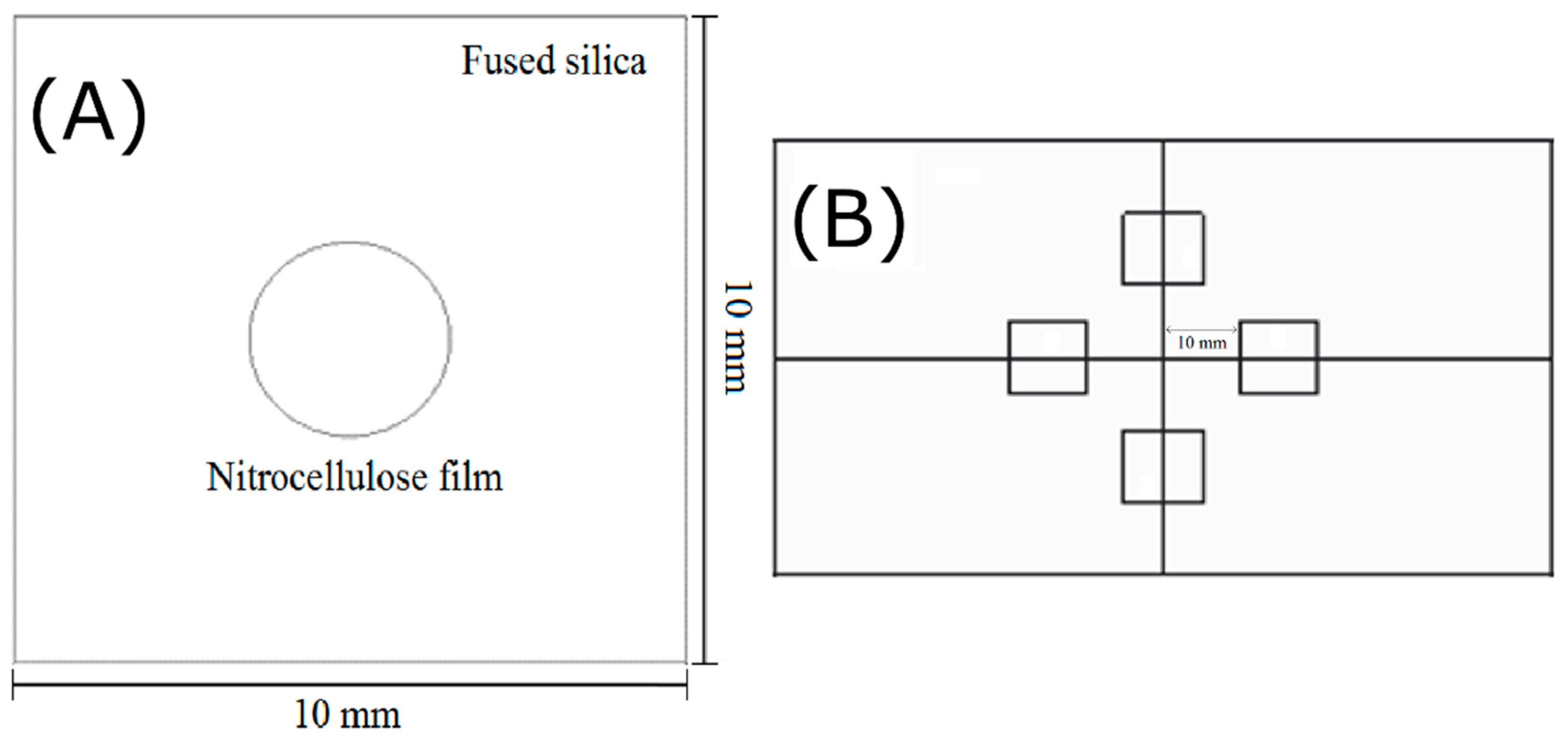
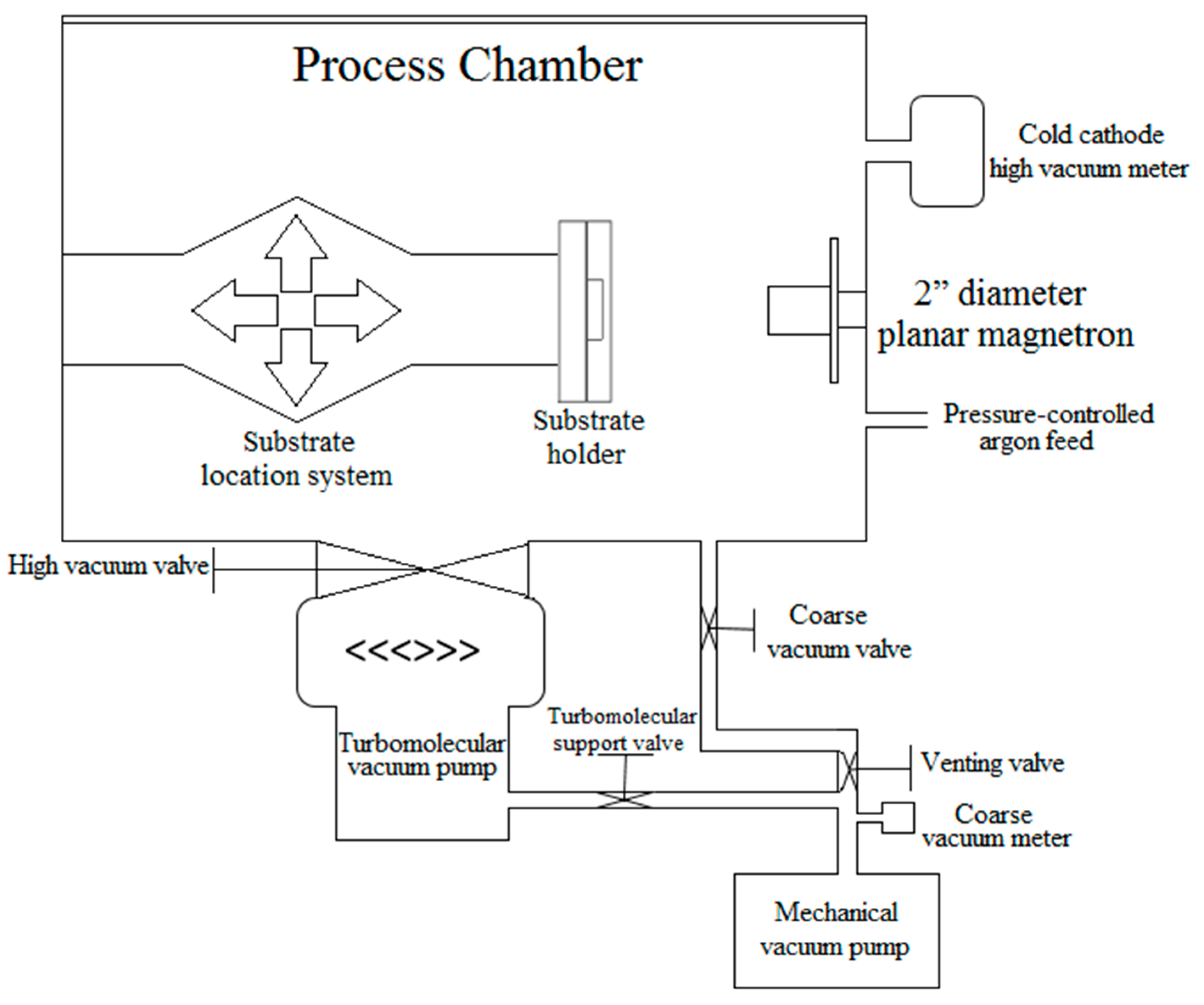
2. Experimental Details

In this work, all Al-NPs growth was carried out using a solid aluminum target of 99.99% purity. This target was pulverized in DC sputtering equipment designed and built at the Institute of Physics of the National Autonomous University of Mexico. Figure 1 shows a schematic representation of the sputtering system. The process chamber has an approximate volume of 100 L; this large volume gives enormous flexibility to the substrate location system, which is manually operated. The substrate location system allows us to control the distance from the magnetron to the substrate in a range of 1 to 30 cm with steps of 1 cm, and the substrate position in a square plane of 50 mm side with a precision of 1 mm. The turbomolecular pumping system takes the process chamber to an ultimate pressure of 1 × 10⁻⁵ Torr. The process pressures can be controlled in a range from 1 × 10⁻⁴ to 1 × 10⁻² Torr by means of an automatic argon feeding system, which acts in response to a MKS Instruments Baratron manometer. The DC source, which drives the magnetron, can deliver a power of up to 1 kW in steps of 1 W.
The depositions were made over the surface of three different substrates: (a) quartz, (b) nitrocellulose film mounted on the TEM grid and (c) quartz coated with graphene. The use of these three substrates is simply linked to the characterizations that can be made with each one of them. Nitrocelusose for TEM and SEM observations, quartz coated with graphene exclusively for observations in SEM and pure quartz for ultraviolet-visible-near infrared (UV-Vis-NIR) spectrophotometry. For the cleaning of quartz substrates, a four-stage (trichloroethylene-methanol-acetone-methanol) ultrasonic bath procedure was carried out, each stage with a duration of 5 min. After the cleaning procedure, high purity nitrogen jets were used to dry the substrates. The nitrocellulose film was manufactured using a 3% solution of collodion in pentyl acetate. A drop (≈0.3 mL) of said solution was poured over distilled water and allowed to dry; the dried film was collected using a 50 mesh copper TEM grid. Quartz coated with graphene substrates have a graphene monolayer coverage of approximately 97% and a sheet resistance of 200 Ω□. These substrates were purchased from Chengdu Organic Chemicals Co., Ltd., Chinese Academy of Sciences (Chengdu, China) and were used without prior cleaning.
The characterization of the Al-NPs deposited on nitrocellulose films was carried out by means of transmission electron microscopy (TEM), using a JEOL JEM-2010F FasTEM microscope (JEOL, Tokyo, Japan) operated at 200 kV near the Scherrer focus, with a spherical aberration of 0.5 mm and a theoretical point-to-point resolution of 0.20 nm. TEM images were recorded with a charge-coupled device (CCD) camera and processed with the GATAN digital micrography system (version 3.7.0, Roper Technologies, Inc., Sarasota, FL, USA). Scanning electron microscopy (SEM) was carried out using a field emission ultra-high resolution scanning electron microscope JEOL-JSM-7800F equipped with an Oxford Instruments Energy-dispersive X-ray Spectroscopy (EDS, Oxford Instruments, Abingdon, Oxfordshire, UK) detector and AZtec 2.1 software. The SEM operating voltages fluctuated between 1 and 10 kV depending on the observed substrate. SEM and TEM micrographs were analyzed using a public domain digital image processing program called ImageJ [25,26]. The optical characterization was carried out using an Agilent Cary 5000 UV-Vis-NIR spectrophotometer (equipped with a deuterium arc lamp for the UV section, Agilent Technologies, Cary, NC, USA) in the range of 175 to 3000 nm with steps of 1 nm.

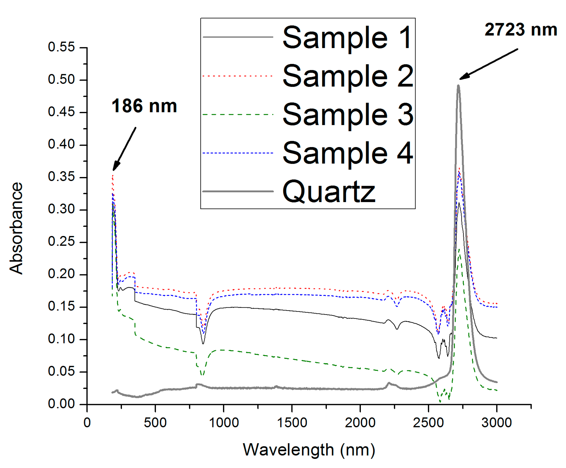
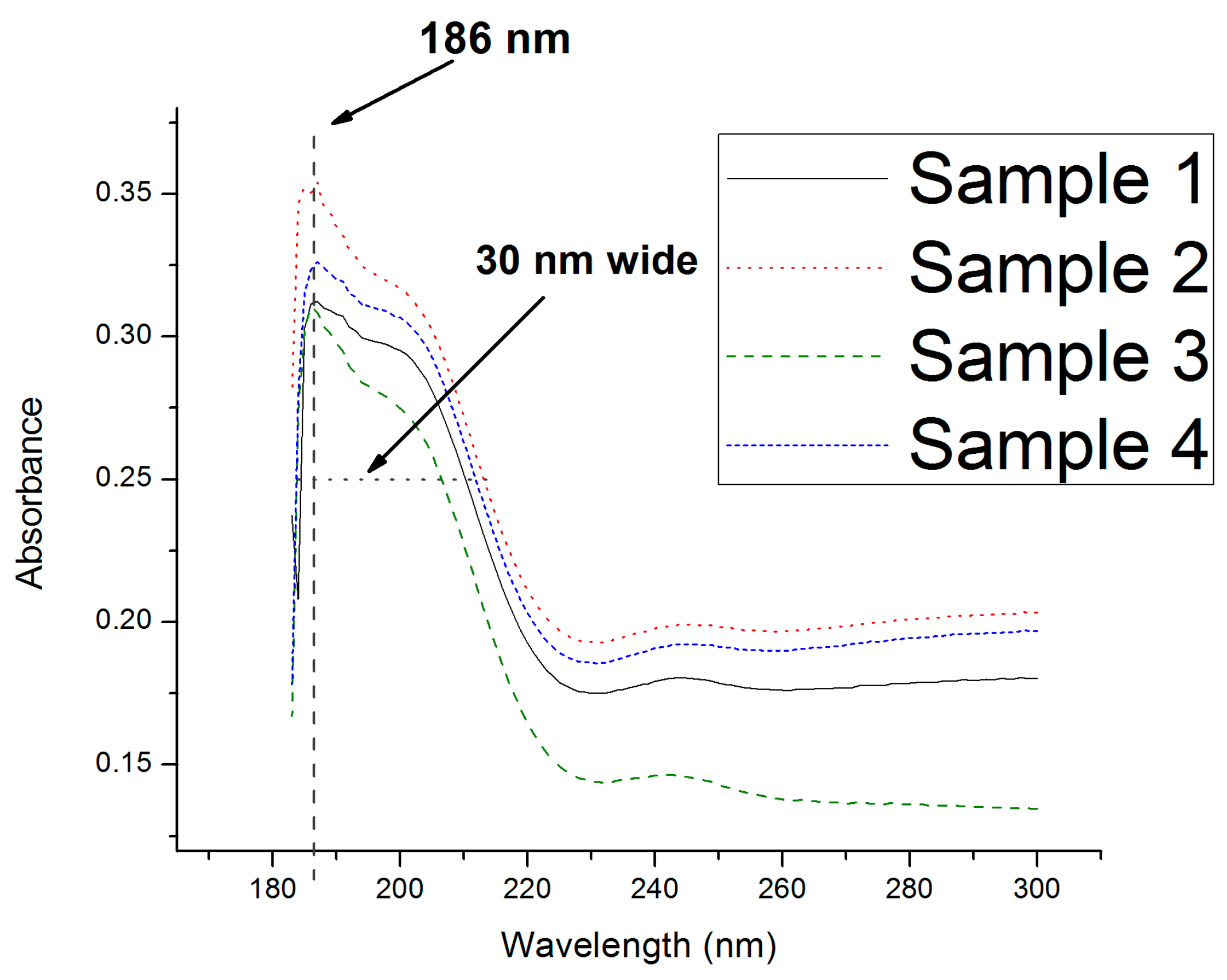
3. Results and Discussion

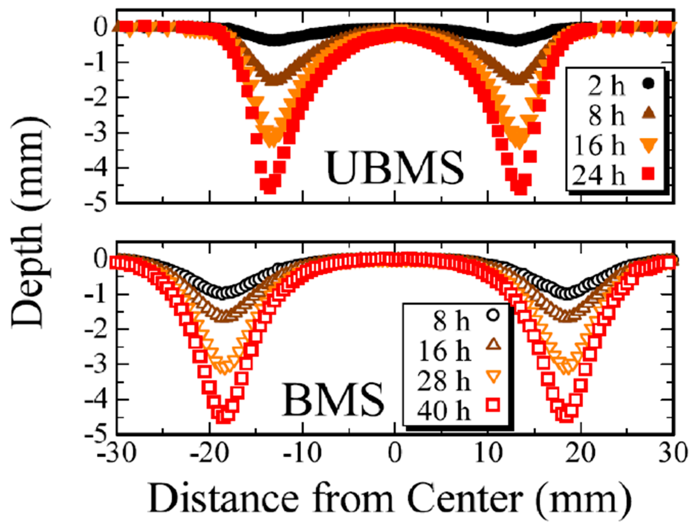
3.1. Determination of Deposition Parameters

As discussed in the introduction, our objective is to conform to exceptional reproducibility for a set of aluminum nanoparticles randomly distributed over the surface of quartz and nitrocellulose substrates through the use of our DC sputtering system (one-step technique). For this endeavor, we made a recursive deposition series followed by a nanostructural characterization.
Recursion was based on the variation of three deposition parameters: (i) deposition time, (ii) distance from the magnetron to the substrate, and (iii) substrate position in the deposition plane. The main task was to vary the deposition parameters until achieving what we have called a successful conformation of aluminum nanoparticles (SCN); which in turn is defined as: A set of aluminum nanoparticles over a solid surface that exhibit the following characteristics: (a) spherical or spheroid particles, (b) random particle distribution, (c) variable average Feret diameter always below 10 nm, and (d) variable inter-particle distance without uncontrolled agglomerations.
To obtain SCN, we follow a three-stage methodology:
Stage I
We performed exploratory depositions using two fixed parameters and three variable parameters. The fixed parameters were pressure at the process chamber of 1.1 mTorr, and a DC power of 100 W. Meanwhile, the initial values of the variable parameters were proposed in the following way: deposition time, 20 s; distance from magnetron to the substrate, 5 cm; and substrate position in the deposition plane, matching the substrate geometric center with the point of greatest erosion in the toroid produced by the ionic roughing from the magnetron, see Figure 2 [27]. This last value is 10 mm from the substrate edge to the substrate-holder geometric center as shown in Figure 3. This position is exclusive for a square substrate of 10 mm side and a balanced circular magnetron of two inches diameter.
Stage II
We carried out a visual inspection and optical microscopy analysis of each exploratory deposition. An SCN on quartz must be imperceptible to the naked eye, while at 1000× in an optical microscope it is possible to identify a very slight change in hue on the quartz surface (increasing in turbidity) [24]. When these two qualitative characteristics were observed, we proceeded to stage III. On the contrary, when the exploratory deposition exhibited turbidity at first glance we proceeded to carry out a new exploratory deposition decreasing the deposition time in steps of 1 s or changing the distance from the magnetron to the substrate in steps of 1 cm until we got the required features.
Stage III
For the depositions that passed stage II, we performed the nanometric characterization by means of SEM and TEM. The characterization was used to obtain information about shape, average Feret diameter and nanoparticle density and distribution. After thirty exploratory depositions, we determined that it is possible to obtain an SCN by using the following parameters: (a) pressure at the process chamber of 1.1 mTorr, (b) DC power of 100 W, (c) a deposition time of 5 s, (d) a distance from the magnetron to the substrate of 13 cm, and (e) a substrate position in the deposition plane as described in Stage I and depicted in Figure 3.

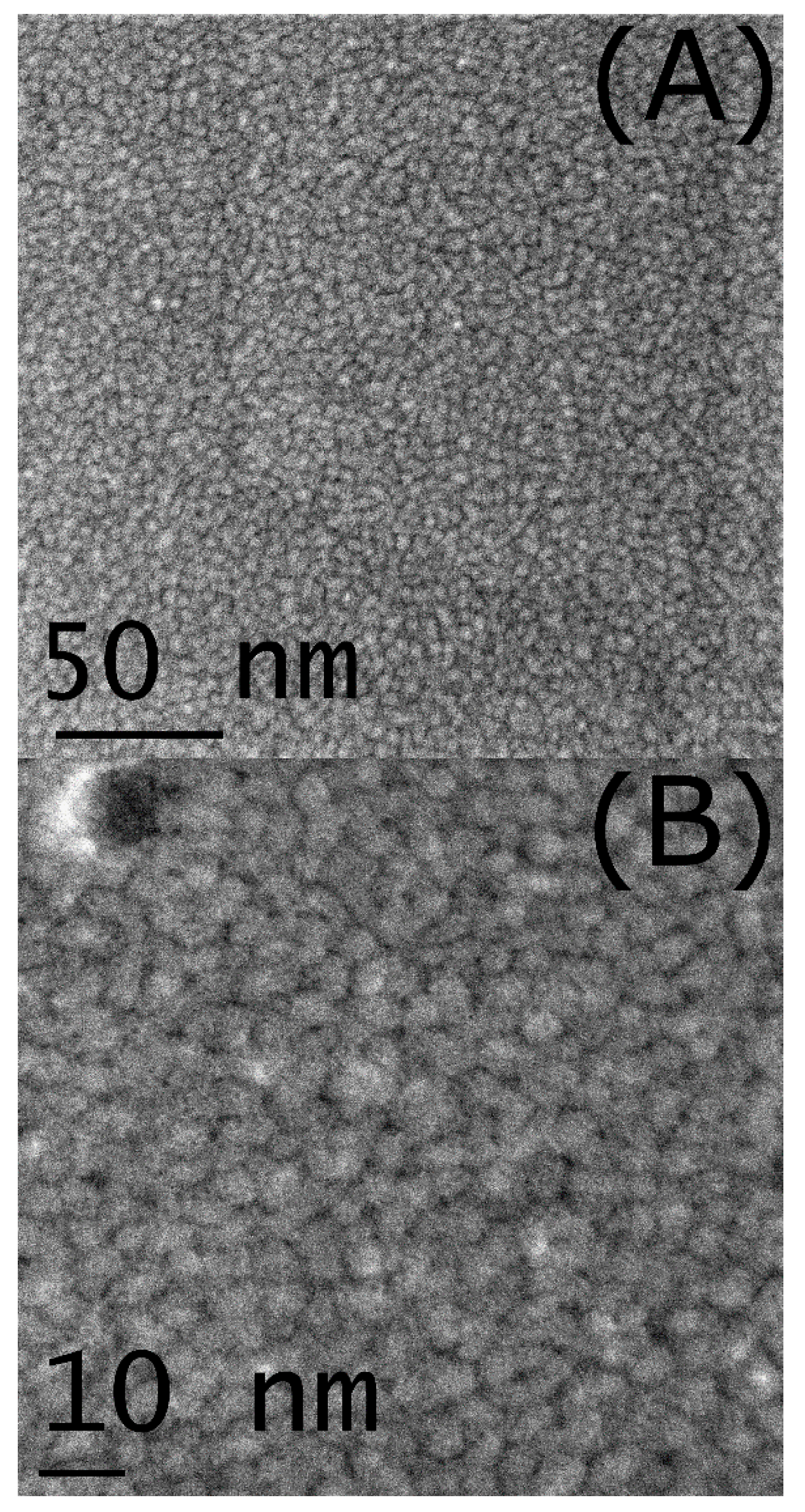
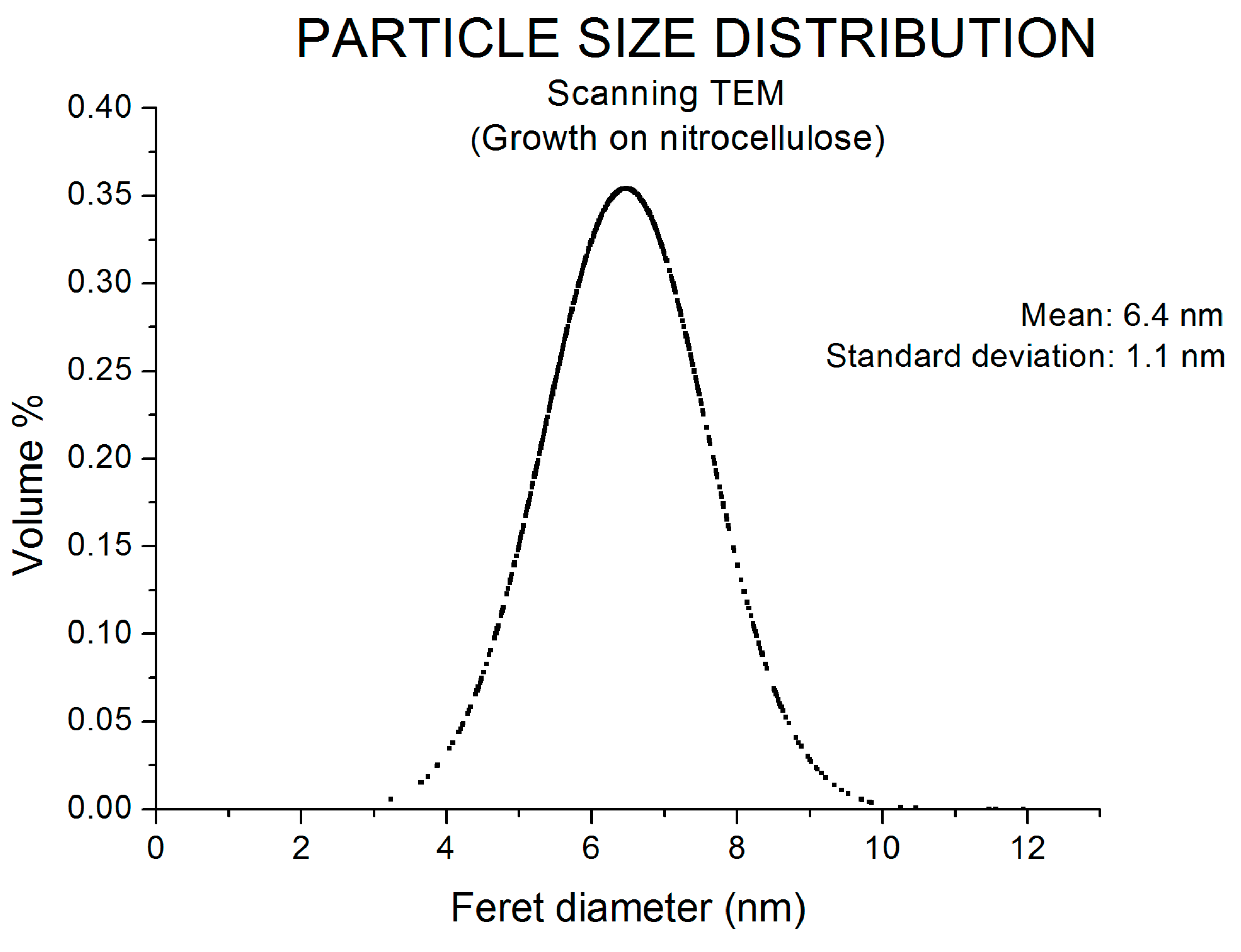
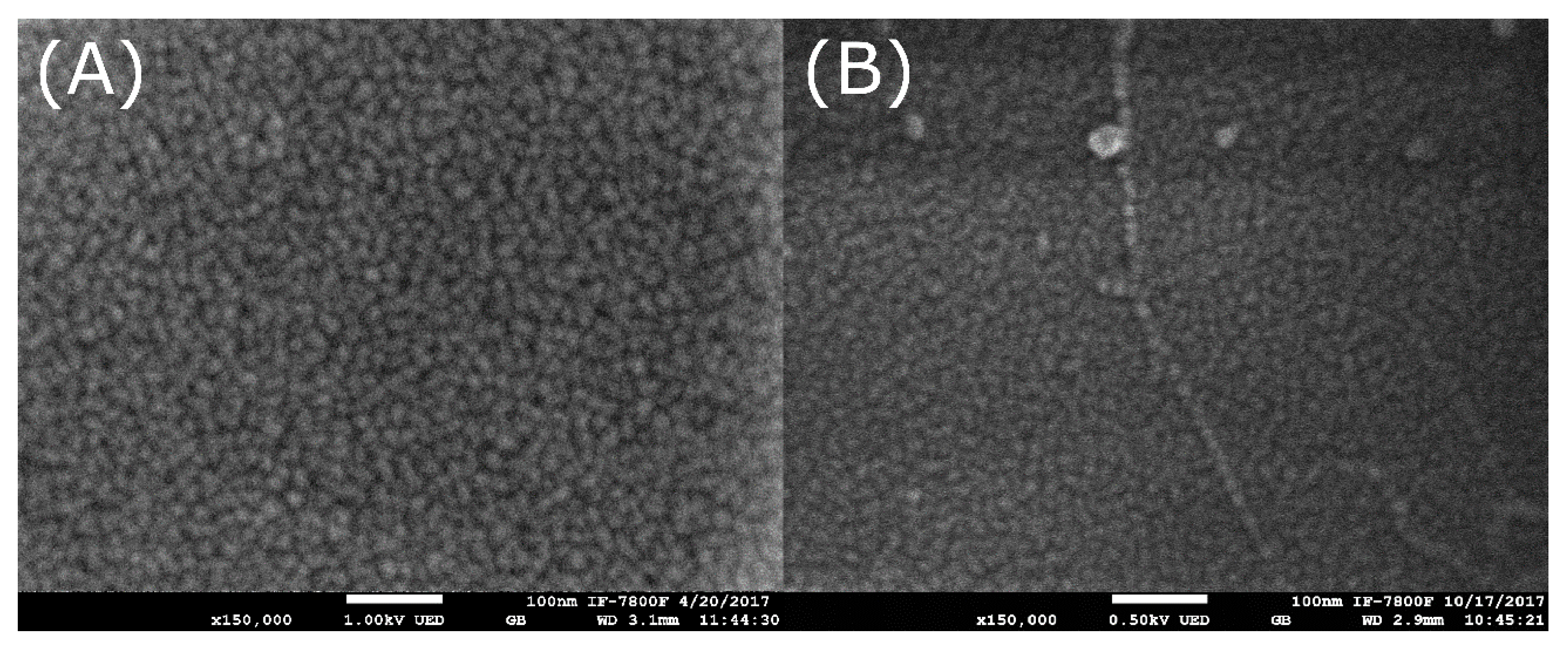
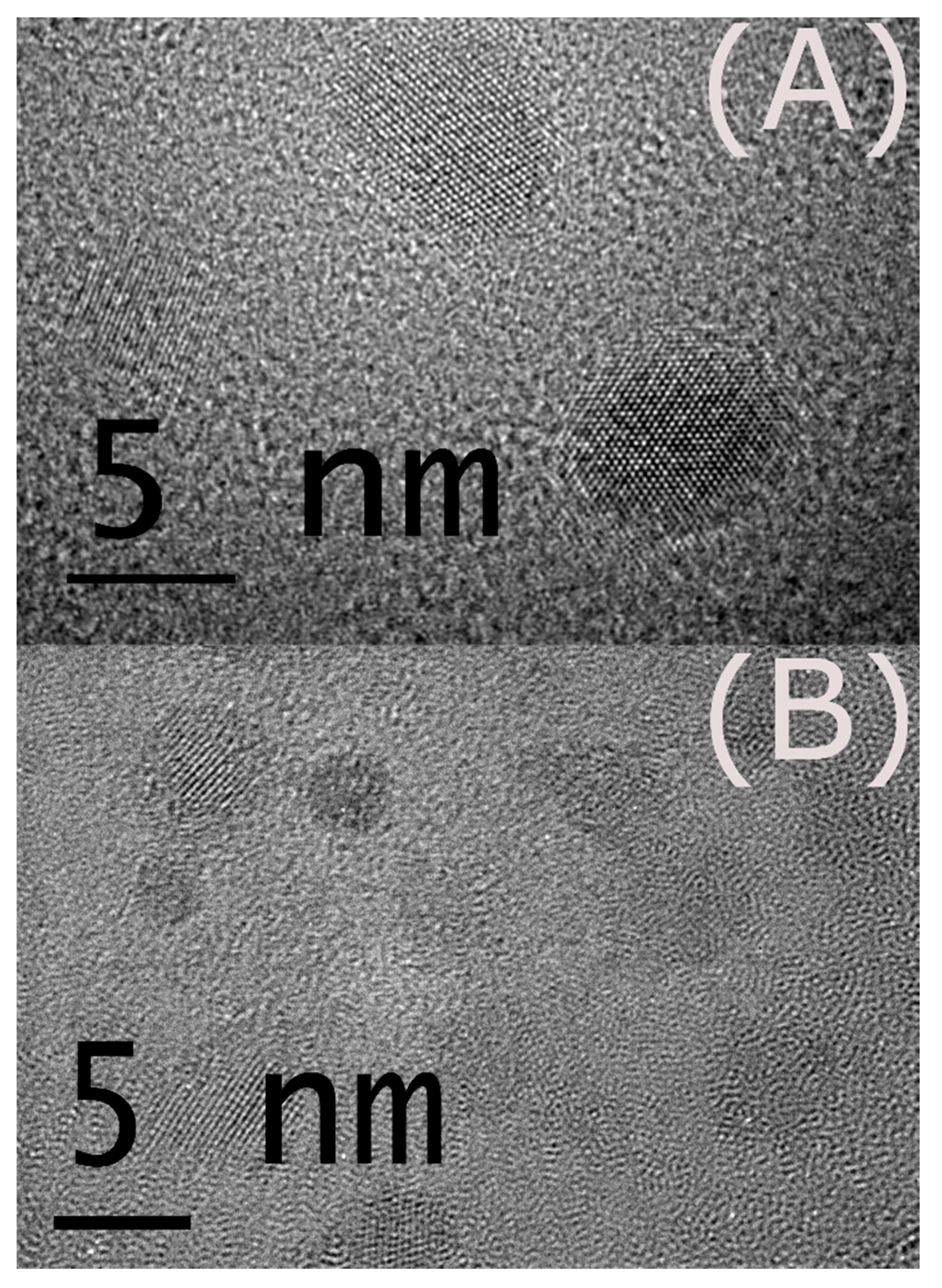
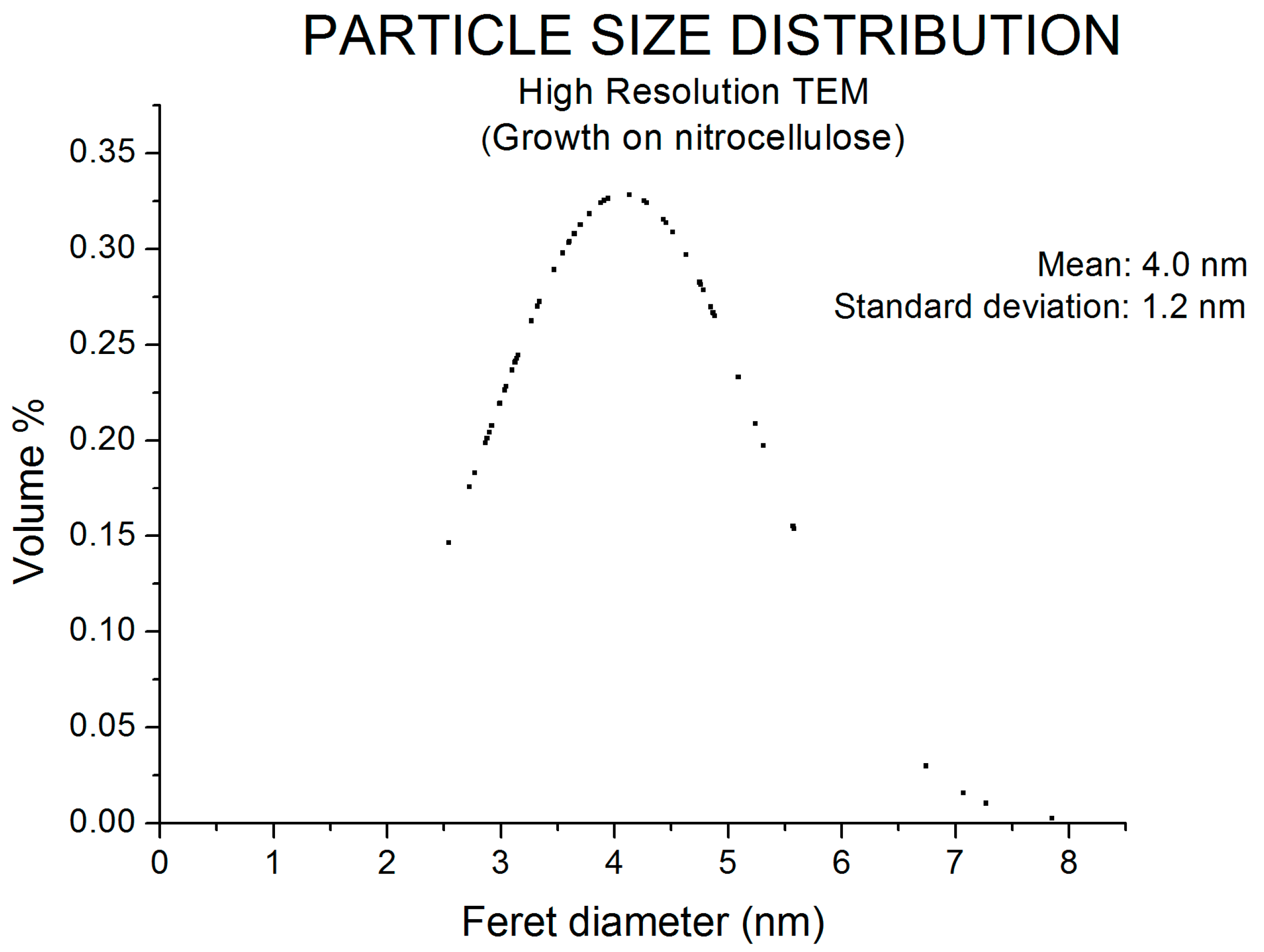
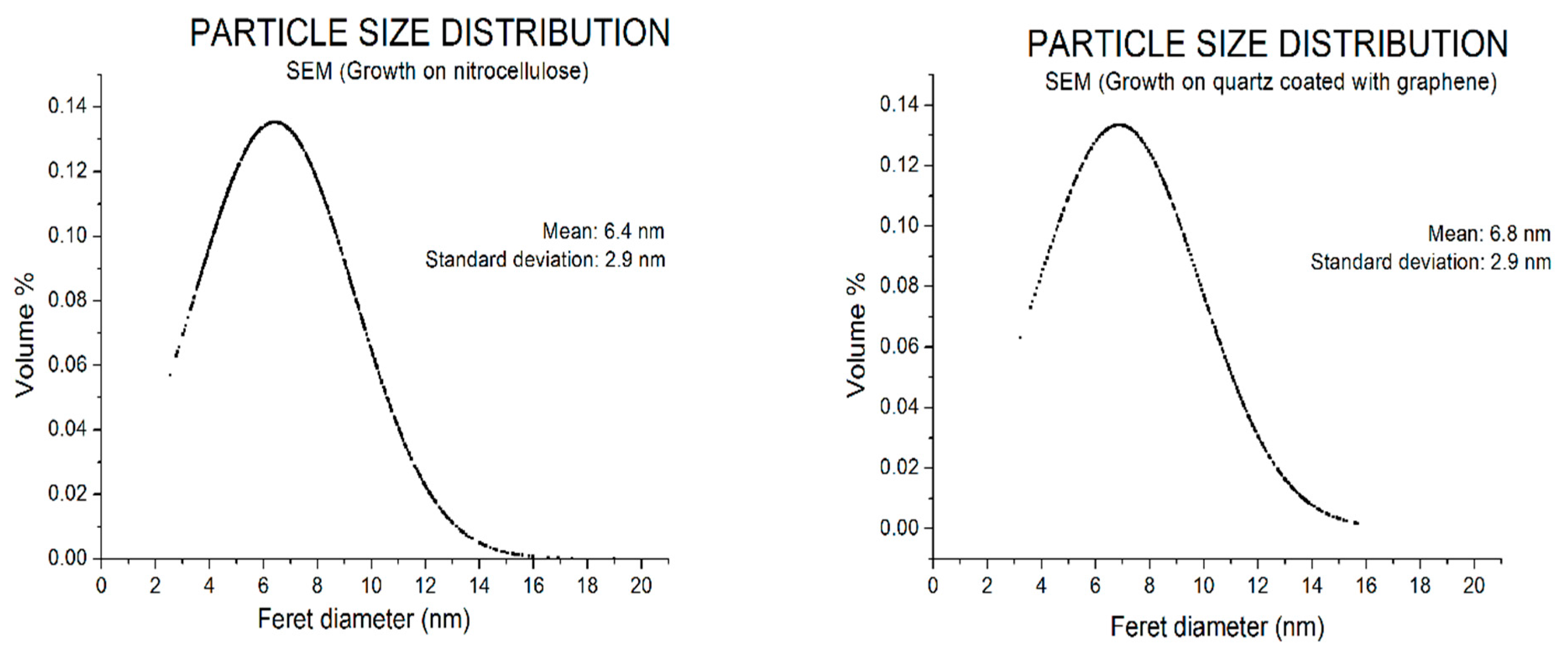
3.2. Nanostructural Characterization

By carrying out the nanostructural characterization, we sought to achieve two goals. First, to prove that for our depositions there is excellent reproducibility at the nanometric scale, i.e., that nanoparticle shape, average size and particle distribution are preserved in each production run. The second is a consequence of the first, and it is to provide the theoretical models with the most precise characteristics of our plasmonic set of aluminum nanoparticles. The above is in order to compare the theoretical predictions with experimental observations in any area where our particles can in the future be studied.
With the deposition parameters that were determined to obtain a successful conformation of aluminum nanoparticles, we made 20 Al-NPs growths, 10 of them on nitrocellulose films and another 10 on quartz substrates coated with graphene. We characterized the depositions through observations in SEM and TEM; later we performed a statistical analysis of the observed particles by means of automatic particle counts made by the ImageJ software [25,26], and through manual particle counts assisted by the GATAN software version 3.7.0.
It is worth noting that we used nitrocellulose film mounted on a copper grid, because on this substrate it is possible to make observations in both TEM and SEM. Meanwhile, graphene-coated quartz substrates allow SEM observations of excellent quality, since the graphene layer on quartz acts as a medium to drain electrons coming from the microscope beam, thus avoiding charge effects. In addition, due to its thickness (≈0.4 nm), graphene does not alter the growth of Al-NPs on quartz [28]. In other words, Al-NP growths on quartz coated with graphene have the same characteristics as Al-NP growths on quartz.
Figure 4 shows two TEM micrographs of an Al-NP sample grown on nitrocellulose. In micrograph (A) a pair of particles in high resolution are shown. In the lower particle appearing in this micrograph it is possible to identify a reticular pattern that could belong to the characteristic face-centered cubic (FCC) crystalline arrangement of aluminum. In that same particle, a discontinuity in its contour can also be identified with some difficulty, and it would indicate the presence of a passivating layer of aluminum oxide (Al2O3) [29]. Meanwhile, micrograph (B) shows an altered distribution of Al-NPs on nitrocellulose. This alteration occurs because the 200 kV of the transmission microscope electron beam generates radiation damage that changed the nanometric configuration of our Al-NPs [30]. The phenomena that we observed when making these observations were the appearance of gaps in the quasi-continuous Al-NP deposition and changes in the sizes and shapes of the Al-NPs [31].
Figure 5 shows the particle size distribution obtained from a statistical analysis carried out using TEM and high resolution TEM (HRTEM) images. The particle count was done manually and using a population sample of 80 particles. For that reason, it is important to note that the results reliability from this analysis is lower than the reliabilities from other statistical analyses presented in this work. Nevertheless, this task was carried out to provide evidence that samples exposed to long periods of radiation, characteristic of high-resolution visualization, alter the nanometric configuration of the sample.
Figure 6 shows two micrographs of Al-NPs deposited on a nitrocellulose substrate at different magnifications. These images were obtained using the scanning TEM technique. In micrograph (A), it is possible to observe particles with a regular spheroidal form that seems to form a continuous thin film. Micrograph (B), at a greater magnification, allows us to distinguish that actually there is no percolation or particle agglomeration. It is clear that the inter-particle distance is less than 1 nm. However, the nature of the scanning TEM technique makes it impossible to accurately determine this distance.
We performed two quick tests that allowed us to glimpse that we are in the presence of a particle distribution and not of an ultra-thin aluminum percolated film. The first was done through a current-voltage test that worked as a high sensitivity continuity test. It was identified that there were no changes in the measurements made on quartz without Al-NPs and the measurements on quartz with Al-NPs. The second was an unfruitful measure of the deposition thickness using a profilometer with 10 nm resolution. Since no results were obtained from the profilometry test, it was inferred that the thickness film was below the resolution thickness of the equipment. In this regard, and considering the average sizes of the Al-NPs, one can estimate that there is a homogeneous particle distribution forming a single layer with a thickness equal to the average nanoparticle size. However, the use of a higher capacity technique such as atomic force microscopy could validate this premise.
In that order of ideas, Figure 7 shows the particle size distribution of Al-NPs deposited on the nitrocellulose film. This size distribution was obtained by means of a statistical analysis carried out automatically using multiple scanning TEM micrographs similar to those shown in Figure 6. It is possible to identify a narrower distribution than that obtained by TEM images, as well as a larger average particle size. Due to the number of particles used to build this particle size distribution, as well as the low damage caused by the scanning TEM technique, we can say that these data have greater reliability.
Thus far we have reviewed the characteristics of the growths of Al-NPs on nitrocellulose substrates. However, it is known that some substrates have an influence on the mechanisms of metal growth, even when using purely physical techniques such as our DC sputtering. For this reason, a statistical analysis of our Al-NPs’ characteristics is necessary in order to prove that they did not suffer any change when the substrate where they are deposited changed, at least for the substrates used in this study.
The first action we took in this direction was the observation of our Al-NPs deposited on quartz by SEM. This is because the nature of the substrate prevents observation by transmission microscopy. No micrographs are reported from the SEM observations on quartz, because charge effects prevented imaging. Nevertheless, as previously mentioned, the use of a graphene layer on the surface of the quartz substrate is imperceptible to the growth mechanism of Al-NPs, and at the same time, graphene allows SEM observation by aiding the attenuation of charge effects. Likewise, it is possible to analyze by SEM the Al-NP growths made on the nitrocellulose film mounted in a TEM grid. Therefore, in Figure 8 we present a comparison of the nanoparticle features observed on nitrocellulose and on quartz coated by graphene when analyzed by SEM.
Qualitatively, it is possible to identify two characteristics. The first is that the nanometric features of the growth performed on nitrocellulose are virtually identical when observed by SEM and when observed by scanning TEM (Figure 6). The second is that the nanometric features of Al-NPs grown on graphene-coated quartz are virtually identical to Al-NP features grown on nitrocellulose. To quantitatively prove these similarities, we performed statistical analyses of both growths.
Figure 9 shows the particle size distribution of Al-NPs grown on the two substrates and observed by SEM. For both samples, 2000 particle populations were used, and they were counted automatically. It is possible to identify that the Al-NPs average size was between 6.4 and 6.8 nm, with a standard deviation of 2.9 nm. The latter allows us to affirm conclusively that our deposits are a set of nanoparticles with spheroidal forms uniformly distributed over the surface of our studied substrates. Those particles have an average diameter of less than 10 nm and are indeed highly reproducible from a nanostructural point of view.

3.3. Optical Characterization

Techniques such as electron energy loss spectroscopy (EELS) with high spatial resolution can evaluate the plasmonic resonances of even a single nanoparticle [30,32]. However, when evaluating the plasmonic resonances of a set of metal nanoparticles by means of a spectroscopic technique such as UV/Vis/NIR, the low spatial resolution exhibited by the vast majority of spectrophotometers (approximately 3 mm spot size) must be considered. In these measurements, what is observed is a collective phenomenon i.e., the beam of the equipment is exciting several million nanoparticles at a time. That is why the reproducibility in the absorbance spectra offers strong proof that there is homogeneity at the millimeter level. Furthermore, it is convenient to mention that is in this size range that a good part of the commercial optical devices operate.
In this sense, to evaluate the existence of the homogeneity and at the same time the millimetric reproducibility in our Al-NP depositions, we made growths on quartz substrates in 10 different production runs. Figure 10 shows the absorbance spectra of four samples taken at random from all the deposited samples in different production runs.
Three characteristics are remarkable. First, the four spectra have identical forms but slight variations in their integrated total absorbance (area under the spectrum). This is due to very slight changes in the thickness of the Al-NP monolayer. It is worth mentioning that the control of those changes is beyond the capacity of any sputtering equipment similar to ours.
Second, an extremely well-defined plasmonic resonance at 186 nm is identified. In previous works it has been reported that this resonance is due to the dipolar mode for particles smaller than 10 nm [7,22]. In those works, it is discussed that for quasi-spherical particles with sizes less than 10 nm deposited or embedded in silica, a resonance is expected to occur around 180 nm. The above is congruent with the resonance reported in Figure 10. Furthermore, in those works it is also proposed that this dipolar mode resonance is insensitive to the size distribution of the Al-NPs. In other words, the average size of the Al-NPs does not matter, if they are below 10 nm the well-defined resonance will appear. Even more striking is the fact that even when a passivating layer of aluminum oxide (Al2O3) is formed on the surface of all the particles, the resonance is going to be observed if the oxide layer is within certain limits [29].
Thirdly, a peak was identified at 2723 nm. This peak is not a plasmonic resonance, but an absorption in the short-wavelength infrared due to the electronic grade quartz substrate used in this study [33]. For the above reasons, we can state that for our depositions a great reproducibility and homogeneity at the nanostructural level extends to the millimetric collective level forming highly homogeneous and of course very reproducible depositions.
Finally, Figure 11 shows the UV section of the absorbance spectra of our samples. We have highlighted with a vertical line the surprising precision shown by the resonance locations of the four different samples. We have also marked the width of the dipolar mode resonance; this width of only 30 nm could confer high sensitivity to optical sensors that were manufactured by using our Al-NP depositions [1,34]. Sensitivity is the smallest absolute change that can be detected by a measurement. In the case of sensors based on plasmonic resonances, it has been observed that sharp resonances give rise to an increase in sensitivity because they are capable of detecting smaller changes. For example, some silver nanoprism arrays have resonances with a full-width at half-maximum (FWHM) of the order of 100 nm, whereas the resonance of our aluminum samples have a FWHM of only 30 nm. Therefore, one could expect, theoretically, a higher sensitivity.

4. Conclusions

In this work, we tackled one of the main technical challenges presented by aluminum plasmonics, namely the trade-off between obtaining nanostructures with highly reproducible plasmonic resonances and the ease of their manufacture. We proved that it is possible to determine optimum deposition parameters, such that by using the magnetron sputtering technique, plasmonic systems with well-defined and reproducible resonances can be obtained. In particular, we grew an aluminum nanoparticle monolayer of Al-NPs with average diameters below 10 nm. The nanoparticle set is uniformly distributed over the surface of quartz and nitrocellulose substrates. We identified that there is great reproducibility at the nanostructural level and we prove by means of absorbance measurements that this reproducibility extends to millimeter scales. Our easy-to-manufacture plasmonic systems have great potential for the construction of optical sensors.

Acknowledgments

All authors would like to acknowledge the technical assistance in SEM and TEM observations and analysis to Samuel Tehuacanero Cuapa. All funding for the realization and publication of this research work came from the projects: (a) Investigación Científica Básica SEP—CONACYT 2016, project number: 283492 and (b) PAPIIT-UNAM, project number IA102718, which are under technical administration of Arturo Rodríguez-Gómez.

Author Contributions

Héctor de Jesús Cruz-Manjarrez made the exploratory and recursive depositions of all the Al-NPs films reported in this work. María del Pilar Aguilar-Del-Valle performed the optical and nanostructural characterization of the Al-NPs depositions. Arturo Rodríguez-Gómez conceived the study and obtained the funding to carry out it; made the analysis of the results and wrote the paper.

Conflicts of Interest

The authors declare no conflict of interest.

References

  1. Homola, J.; Yee, S.S.; Gauglitz, G. Surface plasmon resonance sensors: Review. Sens. Actuators B Chem. 1999, 54, 3–15. [Google Scholar] [CrossRef]
  2. Chen, S.; Zhao, Q.; Zhang, L.; Wang, L.; Zeng, Y.; Huang, H. Combined detection of breast cancer biomarkers based on plasmonic sensor of gold nanorods. Sens. Actuators B Chem. 2015, 221, 1391–1397. [Google Scholar] [CrossRef]
  3. Tao, H.; Lin, Y.; Yan, J.; Di, J. A plasmonic mercury sensor based on silver-gold alloy nanoparticles electrodeposited on indium tin oxide glass. Electrochem. Commun. 2014, 40, 75–79. [Google Scholar] [CrossRef]
  4. Naik, G.V.; Shalaev, V.M.; Boltasseva, A. Alternative plasmonic materials: Beyond gold and silver. Adv. Mater. 2013, 25, 3264–3294. [Google Scholar] [CrossRef] [PubMed]
  5. Knight, M.W.; King, N.S.; Liu, L.; Everitt, H.O.; Nordlander, P.; Halas, N.J. Aluminum for plasmonics. ACS Nano 2014, 8, 834–840. [Google Scholar] [CrossRef] [PubMed]
  6. Rakić, A.D. Algorithm for the determination of intrinsic optical constants of metal films: Application to aluminum. Appl. Opt. 1995, 34, 4755–4767. [Google Scholar] [CrossRef] [PubMed]
  7. Ekinci, Y.; Solak, H.H.; Löffler, J.F. Plasmon resonances of aluminum nanoparticles and nanorods. J. Appl. Phys. 2008, 104, 083107. [Google Scholar] [CrossRef]
  8. Taguchi, A.; Saito, Y.; Watanabe, K.; Yijian, S.; Kawata, S. Tailoring plasmon resonances in the deep-ultraviolet by size-tunable fabrication of aluminum nanostructures. Appl. Phys. Lett. 2012, 101, 081110. [Google Scholar] [CrossRef]
  9. Hu, J.; Chen, L.; Lian, Z.; Cao, M.; Li, H.; Sun, W.; Tong, N.; Zeng, H. Deep-ultraviolet-blue-light surface plasmon resonance of Al and Alcore/Al2O3shell in spherical and cylindrical nanostructures. J. Phys. Chem. C 2012, 116, 15584–15590. [Google Scholar] [CrossRef]
  10. Langhammer, C.; Schwind, M.; Kasemo, B.; Zoric, I. Localized surface plasmon resonances in aluminum nanodisks. Nano Lett. 2008, 8, 1461–1471. [Google Scholar] [CrossRef] [PubMed]
  11. Ekinci, Y.; Solak, H.H.; David, C.; Sigg, H. Bilayer Al wire-grids as broadband and high-performance polarizers. Opt. Express 2006, 14, 2323–2334. [Google Scholar] [CrossRef] [PubMed]
  12. Jha, S.K.; Ahmed, Z.; Agio, M.; Ekinci, Y.; Löffler, J.F. Deep-UV surface-enhanced resonance Raman scattering of adenine on aluminum nanoparticle arrays. J. Am. Chem. Soc. 2012, 134, 1966–1969. [Google Scholar] [CrossRef] [PubMed]
  13. Thyagarajan, K.; Rivier, S.; Lovera, A.; Martin, O.J.F. Enhanced second-harmonic generation from double resonant plasmonic antennae. Opt. Express 2012, 20, 12860–12865. [Google Scholar] [CrossRef] [PubMed]
  14. Kochergin, V.; Neely, L.; Jao, C.Y.; Robinson, H.D. Aluminum plasmonic nanostructures for improved absorption in organic photovoltaic devices. Appl. Phys. Lett. 2011, 98, 133305. [Google Scholar] [CrossRef]
  15. Langhammer, C.; Zorić, I.; Kasemo, B.; Clemens, B.M. Hydrogen storage in Pd nanodisks characterized with a novel nanoplasmonic sensing scheme. Nano Lett. 2007, 7, 3122–3127. [Google Scholar] [CrossRef] [PubMed]
  16. Schwind, M.; Langhammer, C.; Kasemo, B.; Zorić, I. Nanoplasmonic sensing and QCM-D as ultrasensitive complementary techniques for kinetic corrosion studies of aluminum nanoparticles. Appl. Surf. Sci. 2011, 257, 5679–5687. [Google Scholar] [CrossRef]
  17. Meziani, M.J.; Bunker, C.E.; Lu, F.; Li, H.; Wang, W.; Guliants, E.A.; Quinn, R.A.; Sun, Y.P. Formation and properties of stabilized aluminum nanoparticles. ACS Appl. Mater. Interfaces 2009, 1, 703–709. [Google Scholar] [CrossRef] [PubMed]
  18. Thornton, J.A. Magnetron sputtering: Basic physics and application to cylindrical magnetrons. J. Vac. Sci. Technol. 1978, 15, 171–177. [Google Scholar] [CrossRef]
  19. Ray, K.; Chowdhury, M.H.; Lakowicz, J.R. Aluminum nanostructured films as substrates for enhanced fluorescence in the ultraviolet-blue spectral region. Anal. Chem. 2007, 79, 6480–6487. [Google Scholar] [CrossRef] [PubMed]
  20. Stratakis, E.; Barberoglou, M.; Fotakis, C.; Viau, G.; Garcia, C.; Shafeev, G.A. Generation of Al nanoparticles via ablation of bulk Al in liquids with short laser pulses. Opt. Express 2009, 17, 12650–12659. [Google Scholar] [CrossRef] [PubMed]
  21. Sanz, J.M.; Ortiz, D.; Alcaraz De La Osa, R.; Saiz, J.M.; González, F.; Brown, A.S.; Losurdo, M.; Everitt, H.O.; Moreno, F. UV plasmonic behavior of various metal nanoparticles in the near- and far-field regimes: Geometry and substrate effects. J. Phys. Chem. C 2013, 117, 19606–19615. [Google Scholar] [CrossRef]
  22. Maidecchi, G.; Gonella, G.; Proietti Zaccaria, R.; Moroni, R.; Anghinolfi, L.; Giglia, A.; Nannarone, S.; Mattera, L.; Dai, H.L.; Canepa, M.; et al. Deep ultraviolet plasmon resonance in aluminum nanoparticle arrays. ACS Nano 2013, 7, 5834–5841. [Google Scholar] [CrossRef] [PubMed]
  23. Zhao, J.; Zhang, X.; Yonzon, C.R.; Haes, A.J.; Van Duyne, R.P. Localized surface plasmon resonance biosensors. Nanomedicine 2006, 1, 219–228. [Google Scholar] [CrossRef] [PubMed]
  24. Muñoz-Rosas, A.L.; Rodríguez-Gómez, A.; Arenas-Alatorre, J.A.; Alonso-Huitrón, J.C. Photoluminescence enhancement from silicon quantum dots located in the vicinity of a monolayer of gold nanoparticles. RSC Adv. 2015, 5, 92923–92931. [Google Scholar] [CrossRef]
  25. Schneider, C.A.; Rasband, W.S.; Eliceiri, K.W. NIH Image to ImageJ: 25 years of image analysis. Nat. Methods 2012, 9, 671–675. [Google Scholar] [CrossRef] [PubMed]
  26. Rueden, C.T.; Schindelin, J.; Hiner, M.C.; DeZonia, B.E.; Walter, A.E.; Arena, E.T.; Eliceiri, K.W. ImageJ2: ImageJ for the next generation of scientific image data. BMC Bioinform. 2017, 18, 529. [Google Scholar] [CrossRef] [PubMed]
  27. Nakano, T.; Saitou, Y.; Oya, K. Transient evolution of the target erosion profile during magnetron sputtering: Dependence on gas pressure and magnetic configuration. Surf. Coat. Technol. 2017, 326, 436–442. [Google Scholar] [CrossRef]
  28. Shearer, C.J.; Slattery, A.D.; Stapleton, A.J.; Shapter, J.G.; Gibson, C.T. Accurate thickness measurement of graphene. Nanotechnology 2016, 27, 125704. [Google Scholar] [CrossRef] [PubMed]
  29. Gutierrez, Y.; Ortiz, D.; Sanz, J.M.; Saiz, J.M.; Gonzalez, F.; Everitt, H.O.; Moreno, F. How an oxide shell affects the ultraviolet plasmonic behavior of Ga, Mg, and Al nanostructures. Opt. Express 2016, 24, 20621–20631. [Google Scholar] [CrossRef] [PubMed]
  30. Tehuacanero-Cuapa, S.; Reyes-Gasga, J.; Rodríguez-Gómez, A.; Bahena, D.; Hernández-Calderón, I.; García-García, R. The low-loss EELS spectra from radiation damaged gold nanoparticles. J. Appl. Phys. 2016, 120, 164302. [Google Scholar] [CrossRef]
  31. Tehuacanero-Cuapa, S.; Reyes-Gasga, J.; Brès, E.F.; Palomino-Merino, R.; García-García, R. Holes drilling in gold and silver decahedral nanoparticles by the convergent beam electron diffraction electron beam. Radiat. Eff. Defects Solids 2014, 169, 838–844. [Google Scholar] [CrossRef]
  32. Stöckli, T.; Bonard, J.-M.; Stadelmann, P.-A.; Châtelain, A. EELS investigation of plasmon excitations in aluminum nanospheres and carbon nanotubes. Z. Phys. D 1997, 40, 425–428. [Google Scholar] [CrossRef]
  33. Brown, R.N.; Kahan, A. Optical absorption of irradiated quartz in the near IR. J. Phys. Chem. Solids 1975, 36, 467–476. [Google Scholar] [CrossRef]
  34. Anker, J.N.; Hall, W.P.; Lyandres, O.; Shah, N.C.; Zhao, J.; Van Duyne, R.P. Biosensing with plasmonic nanosensors. Nat. Mater. 2008, 7, 442–453. [Google Scholar] [CrossRef] [PubMed]
Figure 1. Schematic diagram of the direct current (DC) sputtering system used to grow the aluminum nanoparticles studied in this work. All vacuum valves and the substrate location system are manually operated. The access to the process chamber is through a big upper lid indicated in the diagram by a double line above the caption “Process Chamber”.
Metals 08 00067 g001
Figure 2. Examples of the erosion profile evolution: Cu target sputtered at 2.0 Pa and DC power of 100 W. Upper: unbalanced magnetron sputtering (UBMS) configuration, Lower: balanced magnetron sputtering (BMS) configuration. “Reprinted from Surface & Coatings Technology, Volume 326, Part B, Takeo Nakano, Yudai Saitou, and Kei Oya, Transient evolution of the target erosion profile during magnetron sputtering: Dependence on gas pressure and magnetic configuration, 436–442, Copyright (2017), with permission from Elsevier” [27].
Metals 08 00067 g002
Figure 3. Schematic representation of the substrates position at the deposition plane: (A) geometry and dimensions of the substrates used in this work. When the depositions were made on nitrocellulose film mounted on the TEM (transmission electron microscopy) grid, the grid was placed at the geometric center of a quartz substrate; (B) substrate-holder at the deposition plane. The substrate-holder geometric center coincides with the magnetron geometrical center. In the shown configuration, the geometric centers of the four substrates coincide with the maximum erosion point of the roughing toroid of a two inches diameter magnetron.
Metals 08 00067 g003
Figure 4. Transmission electron microscopy micrographs of a set of aluminum nanoparticles grown on nitrocellulose. Micrograph (A) is high resolution, and reticular patterns can be identified in the two presented particles. Micrograph (B) shows a greater number of particles, those particles are altered in their distribution and sizes due to the radiation effects of the electron beam generated at 200 kV.
Metals 08 00067 g004
Figure 5. Particle size distribution of Al-NPs (aluminum nanoparticles) grown on nitrocellulose. The statistics were made using TEM and HRTEM micrographs and counting a population of 80 particles manually. It is possible to observe a quasi-normal particle distribution. The obtained average Feret diameter was 4.0 nm with a standard deviation of 1.2 nm.
Metals 08 00067 g005
Figure 6. Scanning TEM micrographs from a set of Al-NPs deposited on nitrocellulose. Different magnifications of the same sample are shown. (A) Due to the nature of the scanning TEM technique there seems to be a percolation in the growth. (B) However, there are uniformly distributed quasi-spherical particles with inter-particle distances less than 1 nm.
Metals 08 00067 g006
Figure 7. Particle size distribution of Al-NPs grown on nitrocellulose. The statistics were made using scanning TEM micrographs and counting a population of more than 1000 particles automatically. It is possible to observe a quasi-normal particle distribution. The obtained average Feret diameter was 6.4 nm with a standard deviation of 1.1 nm.
Metals 08 00067 g007
Figure 8. SEM images of aluminum nanoparticles monolayer deposited on: (A) TEM grid coated with nitrocellulose and (B) quartz coated with graphene. A magnification of 150,000× and a scale bar of 100 nm is presented for both samples. In both micrographs, particle growth with identical quasi-spherical morphology is observed.
Metals 08 00067 g008
Figure 9. Particle size distribution of Al-NPs grown on nitrocellulose (left) and quartz coated with graphene (right). The statistics were made using SEM micrographs and counting a population of more than 1000 particles automatically. In both samples, a quasi-normal particle distribution was observed. The similitude of the average Feret diameters and standard deviations confirms that the growths are equal in both substrates.
Metals 08 00067 g009
Figure 10. Absorbance spectra of four samples taken at random from a set of samples deposited in different production runs and a quartz substrate. In the UV section of the spectrum, it is possible to identify a well-defined plasmonic resonance at 186 nm for the four samples. In the short-wavelength infrared section, an absorption at 2723 nm is observed. This peak is not a plasmonic resonance, but an absorption in the short-wavelength infrared due to the electronic grade quartz substrate used in this study [33].
Metals 08 00067 g010
Figure 11. Absorbance spectra of four samples taken at random from a set of samples deposited in different production runs. In this amplification, the location and width characteristics of the dipole mode resonance are identified.
Metals 08 00067 g011

