1. Introduction
Since the invention of wire bonding technology by Bell Laboratories in 1957, Au has become the most popular material for this packaging process. In recent years, the rising cost of Au has created a demand for new bonding wires to replace Au wire. For this purpose, Cu wire and Pd-coated Cu wire are under consideration due to their low cost, high tensile strength, and good electrical and thermal conductivity. However, the inherent tendency of Cu to oxidize restricts its application to wire bonding, for it raises serious concerns about the reliability of electronic products. This concern cannot be completely eliminated, not even by coating Cu wire with Pd, Au, or Pt thin films. Furthermore, in contrast to the overgrowth of intermetallic compounds that occurs at the interface between Au wire and Al pad, the risk of using Cu wire is that an insufficient intermetallics layer may form in the joints, leading to a poor bonding effect [
1,
2]. In addition, the high hardness of Cu wire requires a large bonding force. The use of greater force can cause under-pad chip cratering, especially in the packaging of certain integrated circuit (IC) chips with low K substrates [
3]. It has also been recognized that Cu wire is unsuitable for certain advanced wire bonding technologies, such as the stacking die, bonding ball on stitch (BBOS), or bonding stitch on ball (BSOB) methods.
Recently, Pd- and Au-doped Ag-alloy wires with large amounts of annealing twins have been developed to replace Au and Cu bonding wires in IC and LED packaging [
4,
5]. The addition of Pd and Au into Ag-alloy wire both increases the mechanical strength and improves its oxidation and corrosion resistance. Adding Pd also reduces the electromigration of the pure Ag conductor and inhibits the overgrowth of intermetallic compounds at the interface between the Ag-bonding wire and Al pad. In addition, a new method of multiple drawings interspersed with multiple annealing treatments can produce a high percentage of annealing twinned grains in this Ag-alloy wire. It is known that the low energy of twin boundaries yields many beneficial effects on the mechanical properties of structural materials [
6,
7,
8]. In previous studies, it was verified that annealing twinned Ag-8Au-3Pd and Ag-4Pd alloy wires retain the thermal stability of the grain structure and material properties at elevated temperature for longer than conventional grained wires with fewer twinned grains [
9,
10]. After a further wire bonding process in an electronic package, the high thermal stability of the grain structure in annealing twinned Ag-8Au-3Pd and Ag-4Pd bonding wires results in a smaller heat affected zone (HAZ) near the ball bond than that in conventional grained wires, ensuring the applicability of these Ag-alloy wires to ultra-low loop wire bonding [
11].
During the operation of IC devices, current stressing in the interconnections of packages can cause electromigration, leading to the early wear-out of electronic products. Such a failure mode under current stressing has attracted attention in recent years due to the current trend of minimizing interconnections. Although electromigration has been known to the IC industry for several decades [
12], it has only recently been observed in electronic packages, such as flip chip solder bumps [
13] and ball grid array (BGA) solder joints [
14]. However, few researchers have reported on the effects of current stressing on the grain structure and material properties of bonding wires. Tse and Lach reported a failure case of Al bonding wires in an octal buffer inverter device after a few years of field usage [
15]. They observed a phenomenon of thinning and thickening of the diameter that accompanied the breakage and melting of wire material, which implied that a mass redistribution of Al had occurred due to current stressing. In addition, grain growth of the wire material—even to the development of a special “bamboo” structure—was also observed. Orchard et al. [
16] reported that current stressing indeed accelerated the failure of wire bonding joints. Zin et al. further indicated that the damage caused by electrical current was greater than that caused by thermal aging [
17]. They also found that the growth of intermetallic compounds at the Au/Al interface was more rapid when electrons flowed from Au wire to Al pad than when they flowed in the opposite direction. In contrast, Schepper et al. [
18] and Krabbenborg [
19] reported that current stressing negligibly affected the contact failure of a package with Au wire bonding on Al pad.
It is known that doping Ag-alloy wires with different amounts of Pd and Au can change the electrical conductivity, which affects the temperature of wire materials due to the Joule effect. In addition, the atomic diffusion of Ag-alloy wires with various Pd and Au contents under current stressing can also influence the grain boundary migration. This study therefore examined the effects of the alloy concentrations of Ag-Au-Pd bonding wires under current stressing on their grain structures and the resultant degradation of mechanical properties.
3. Results
Figure 2,
Figure 3,
Figure 4,
Figure 5,
Figure 6 and
Figure 7 show the grain structures in longitudinal cross-sections of the bonding wires after stressing at a current density of 1.23 × 10
5 A/cm
2 for various time periods. It can be seen in
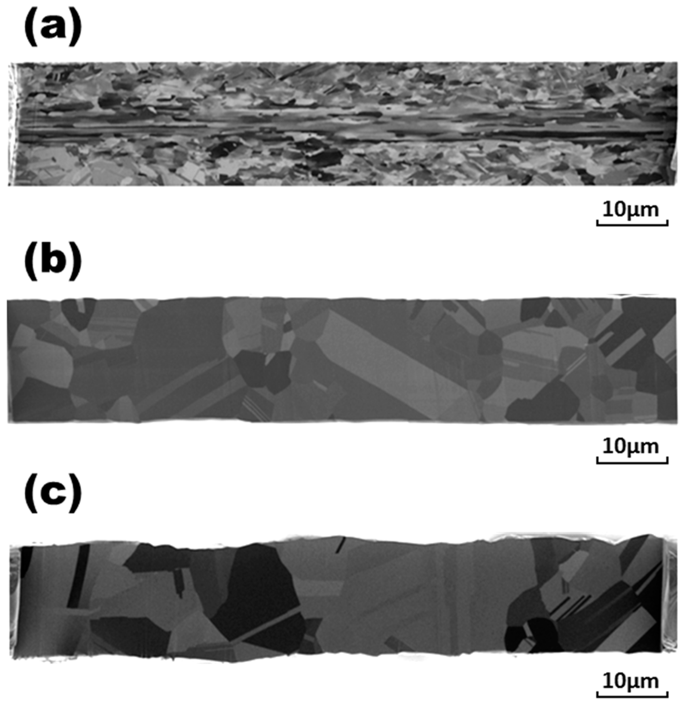
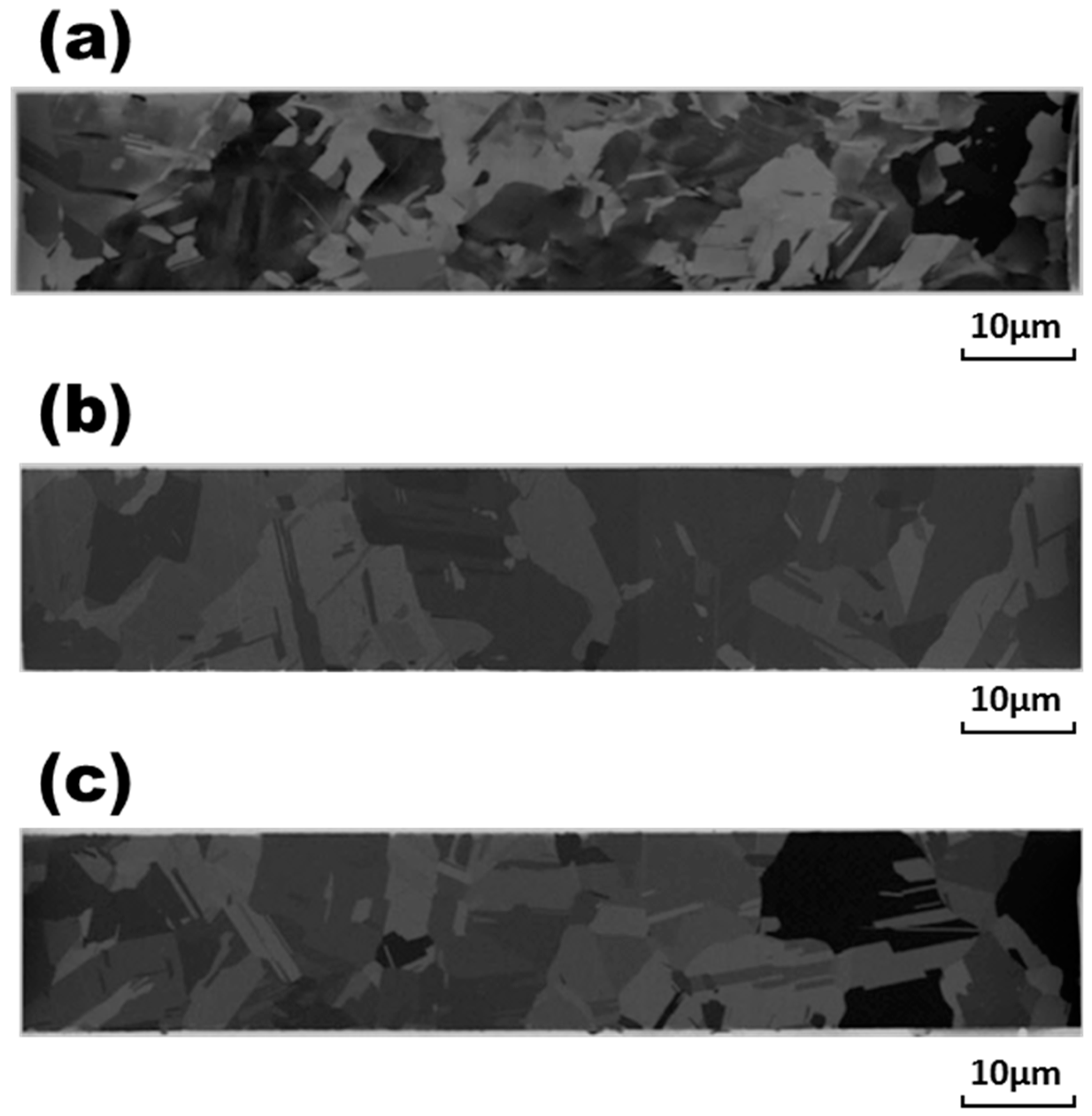
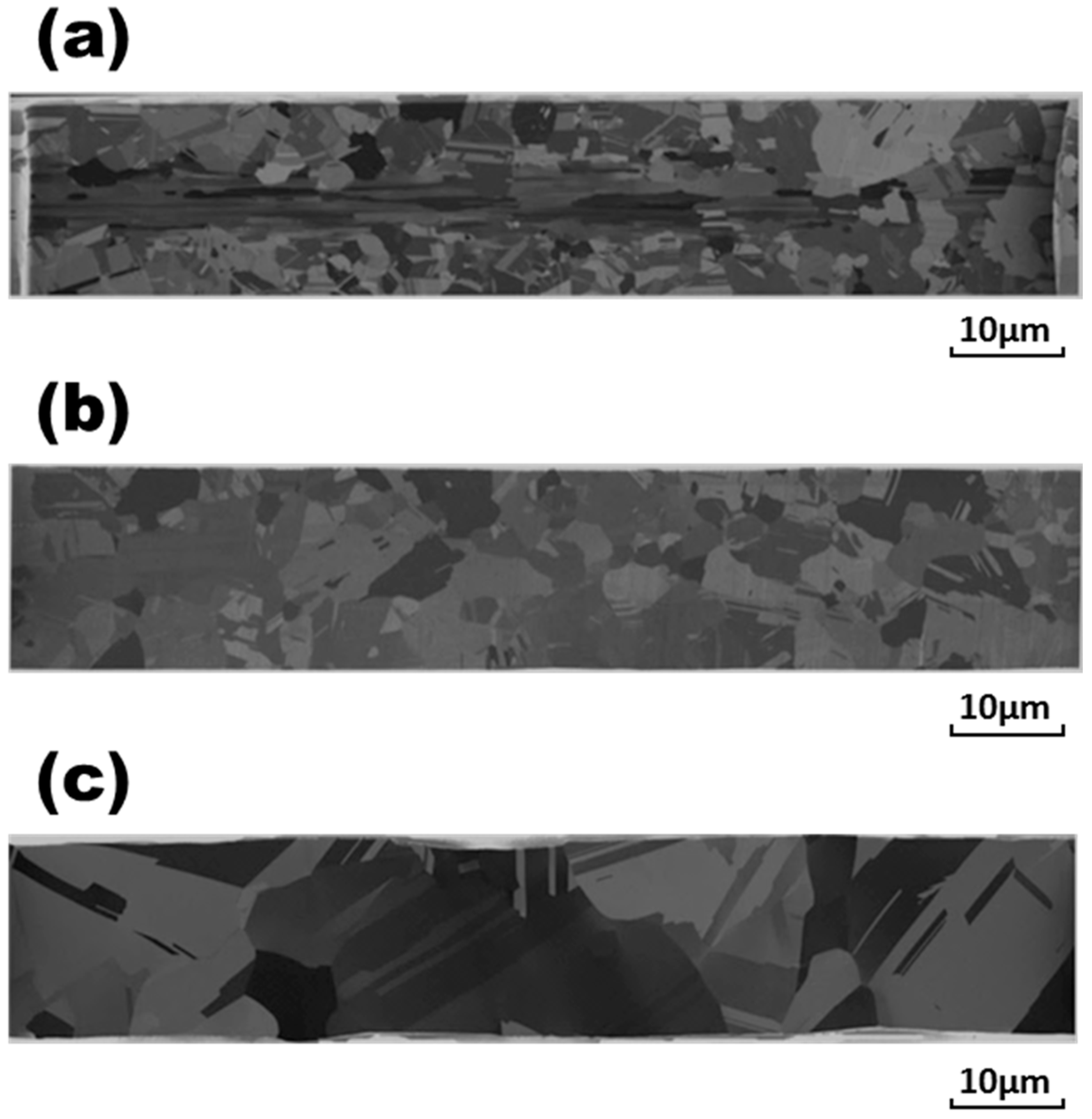
Figure 2a and
Figure 3a that the original bonding wires with compositions of Ag and Ag-0.5Pd comprised equiaxial grains with coarse grain sizes of 6.5 and 9.7 μm, respectively. In
Figure 6a, many equiaxial fine grains of about 1.6 μm with a texture-oriented structure can be observed in the original pure Au wire. In contrast, slender grains appeared in the central parts of Ag-3Pd, Ag-15Au-3Pd, and Pd-coated Cu wires, as shown in
Figure 4a,
Figure 5a and
Figure 7a. Surrounding the central slender grains in these alloy wires were equiaxial fine grains of 6.2, 2.5, and 4.8 μm in size, respectively, with a mass of annealing twins. The finer grain sizes in Ag and Ag-15Au-3Pd, as compared to those of the other bonding wires, indicated that the addition of Au to Ag alloy wires can obstruct recrystallization during the final annealing treatment after the drawing process in the manufacturing of these bonding wires.
During electrical stressing at a current density of 1.23 × 10
5 A/cm
2 for 1 h, the central slender grains in Ag-3Pd, Ag-15Au-3Pd, and Pd-coated Cu wires disappeared, and the equiaxial grains were redistributed throughout the wires, as shown in
Figure 4b,
Figure 5b and
Figure 7b. It can also be seen in
Figure 4 and
Figure 7 that the equiaxial grains in the original Ag-3Pd wire grew from 6.2 μm to 11.9 μm. In contrast to the moderate grain growth in Ag-3Pd wire, the growth of the grains in the pure Ag, Ag-0.5Pd, pure Au, and Pd-coated Cu wires was far more severe, as shown in
Figure 2,
Figure 3,
Figure 6 and
Figure 7. It is obvious that the addition of 3 wt. % Pd in Ag-alloy wires retarded further grain growth during current stressing. However, the grains in Ag-15Au-3Pd wire also grew drastically, from 2.5 μm to 13.7 μm, as evidenced in
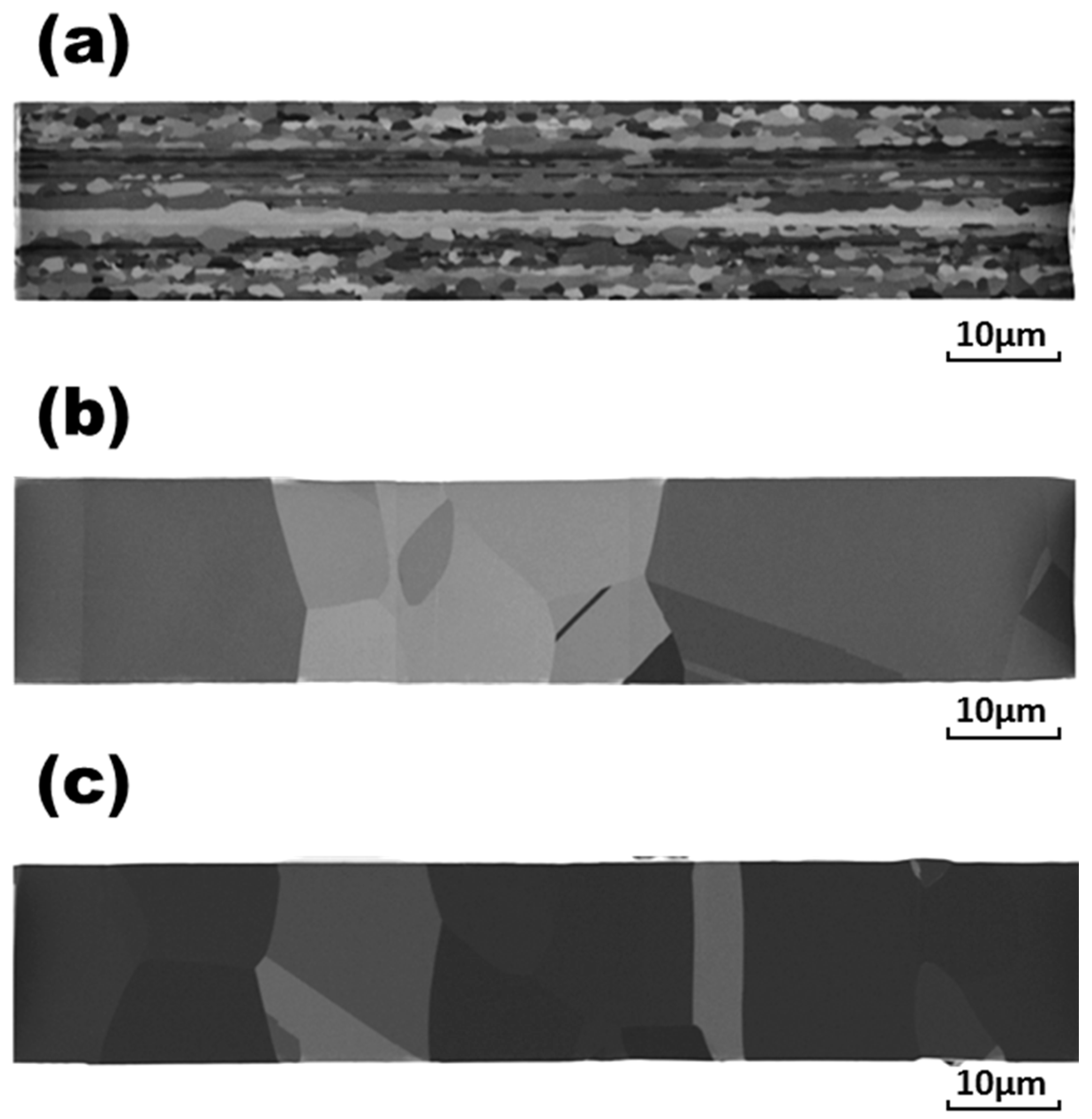
Figure 5a,b, similar to the rapid grain growth in pure Au wire.
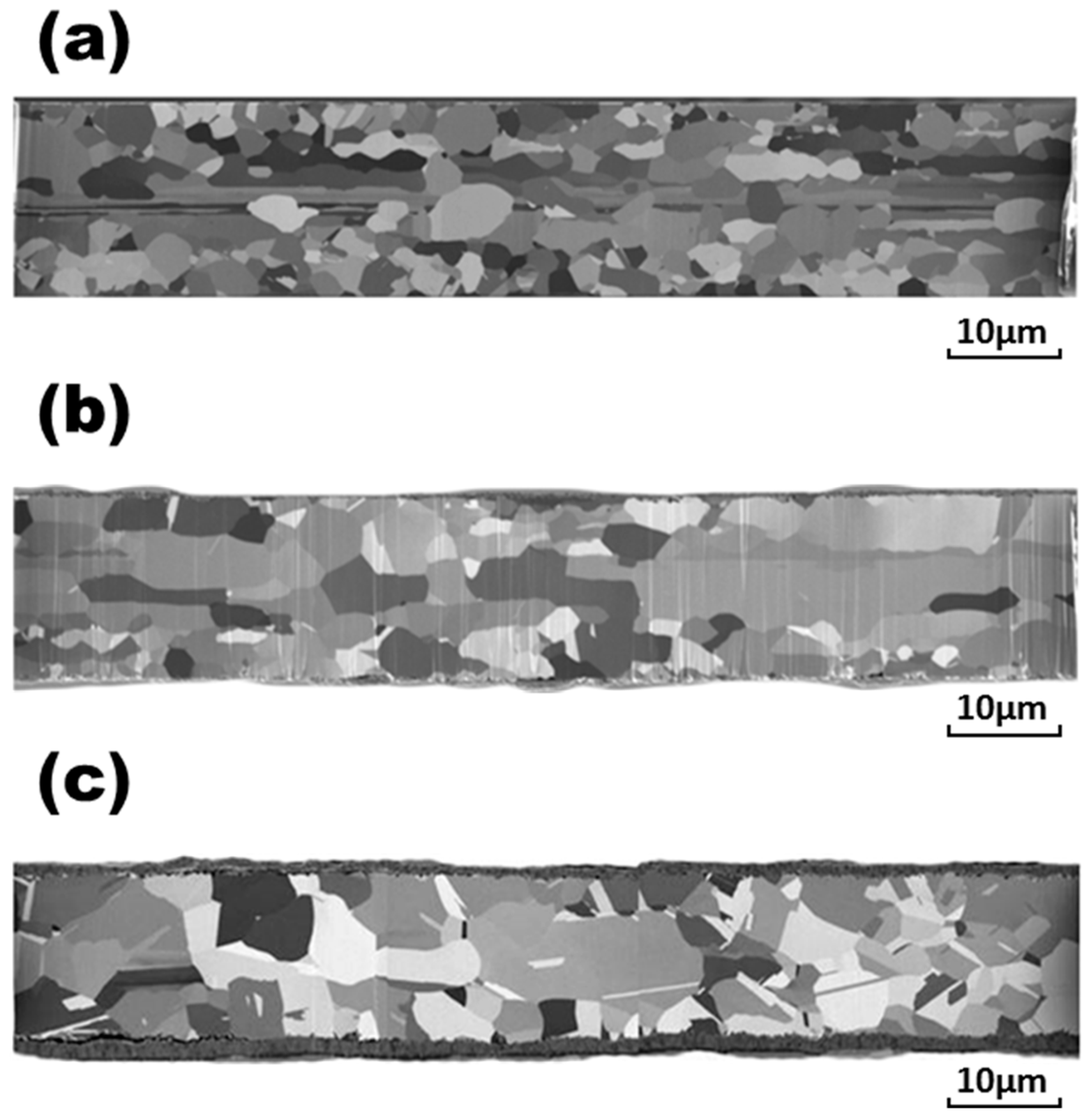
It should be noted here that, during current stressing, the wire temperature increases due to the Joule effect. However, direct measurement of the temperature of wire specimens with a diameter of 17.6 μm (such as those in this study) is quite difficult and prone to inaccuracy. An alternate method for indirectly determining the wire temperature—by measuring its electrical resistivity—was proposed in our previous study [
20]. It was also shown in that report that the temperatures of Ag-15Au-3Pd and pure Au wires were higher than that of Ag-4Pd (similar to the Ag-3Pd), leading to the larger grain structure of the former Au-containing wires than that of the Ag-3Pd. In this study, increasing the stressing time to 20 h caused the grains of all the bonding wires to grow further. However, the growth rates became much slower than those in the early stage of stressing for 1 hr. However, as shown in
Figure 5c and
Figure 6c, the grains in Ag-15Au-3Pd and pure Au even grew into a “bamboo” structure, similar to the phenomenon observed by Tse and Lach [
15] in Al bonding wire. It seems that Au can exaggerate the electromigration of bonding wires and enhance their grain growth effects.
From the observations of grain structures in these bonding wires, it is clear that the electrical current caused recrystallization and grain growth. Although electrical stressing at a current density of 1.23 × 10
5 A/cm
2 can increase the wire temperature to about 100 °C (as reported in our previous study [
20]), it was shown in another of our studies that the grain structure of a wire specimen remained almost unchanged during heating at 200 °C for 50 h in an air furnace without electrical current stressing [
21]. Therefore, it is suggested that the grain growth in the current stressed wires was predominantly caused by the grain boundary motion driven by the electron flow, rather than by recrystallization driven by the thermal effect.
Figure 7b indicates that, for the Pd-coated Cu wire, electrical stressing for 30 min caused an oxide layer of about 1.5 μm to form on its outer surface, and the grain size of this bonding wire increased from 4.8 μm to 13.2 μm. The oxide layer thickened rapidly to about 5.3 μm, as shown in
Figure 7c, and this thickening was accompanied by grain growth to 15.3 μm in the remaining Cu wire when the current stressing time was lengthened to 1 h. The Pd-coated Cu wire was oxidized completely after current stressing for 3 h.
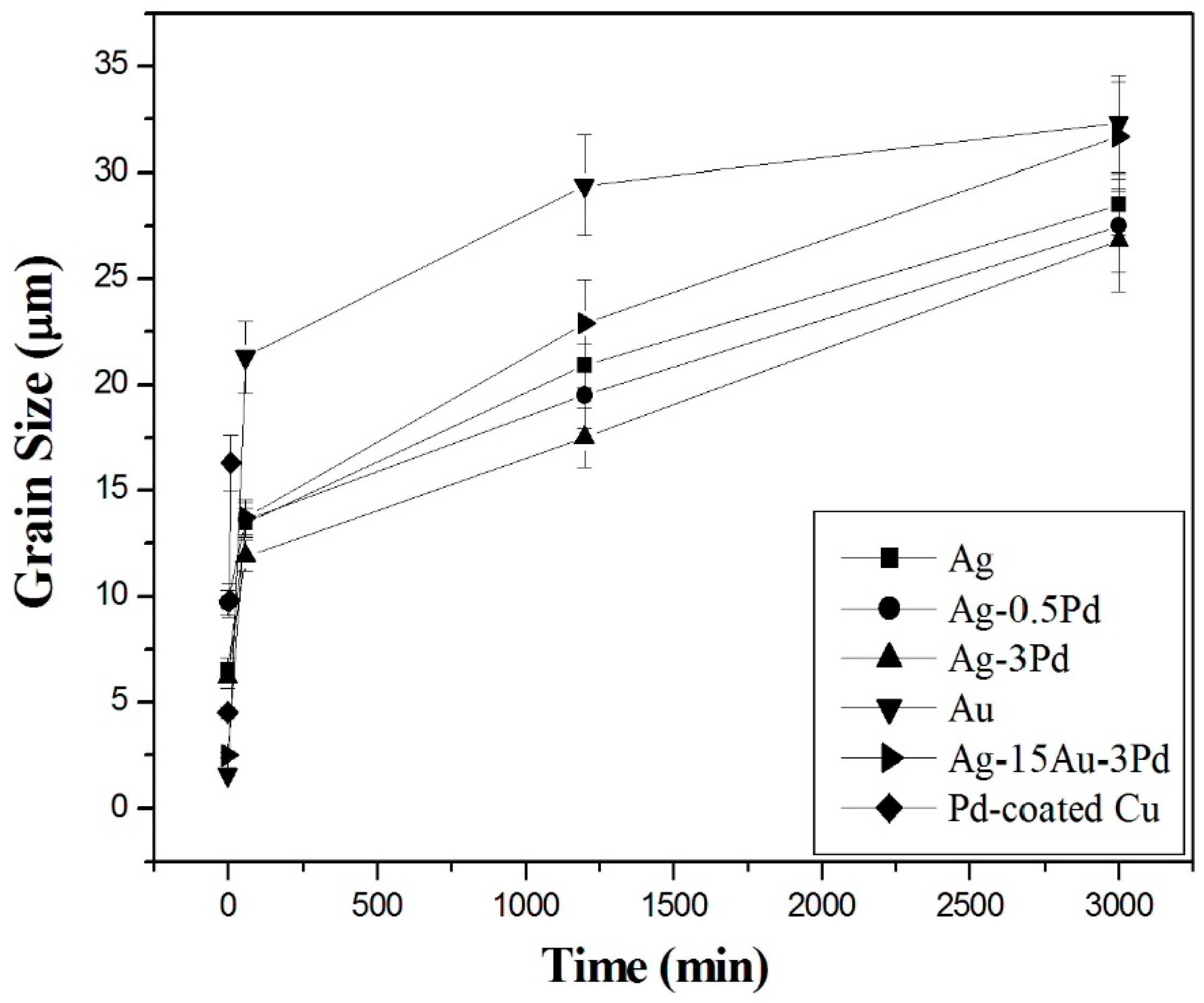
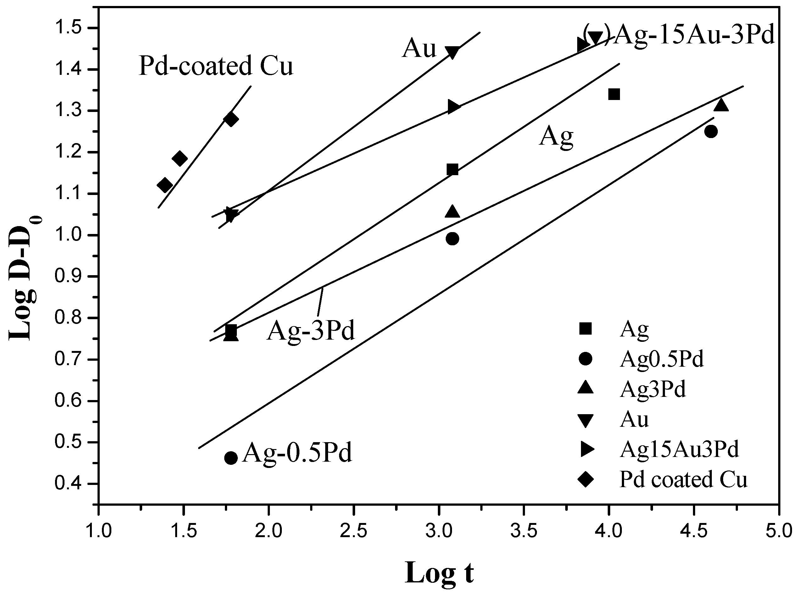
The grain sizes of various bonding wires after current stressing for different time periods are summarized in
Figure 8. The results indicate that grain growth was much more rapid in pure Au and high Au-content Ag-15Au-3Pd wire than in the Ag and Ag-alloy wires. In the Ag-alloy wires, the addition of Pd retarded grain growth. Among all the bonding wires in this study, Ag-3Pd had the finest grains. In addition, the curves in
Figure 8 reveal that the grains of all bonding wires first grew rapidly and then more slowly during current stressing. This kinetic behavior implies that the grain growth rate varies inversely with the grain size, which leads to the relation:
where
D is the mean grain diameter after stressing time (
t) and
K1 is constant, depending on wire composition. When the initial grain diameter (
D0) is much smaller than the grain diameter after various current stressing times (
Dt), the grain growth Equation (1) can be integrated as:
where
n is the grain growth exponent. However, the relation of
n = 0.5 in Equation (2) only exists for a high purity metal and the aging temperatures near its melting point, corresponding to the soap cells model [
22]. In general, the
n values depend on the purity of metals, the aging temperatures, and the texture in this metal [
23]. For the calculation of the grain growth exponent (
n), Equation (2) is expressed in a logarithmic form:
which is plotted in
Figure 9 for various bonding wires. The grain growth exponents (
n) can be calculated from the slopes of the straight lines in
Figure 9, and they are summarized in
Table 1. For the determination of the n value of pure Au wire, it was noticed that after current stressing for 20 h, the grains of pure Au wire had grown to 29.4 μm, which was much larger than the wire diameter (17.6 μm), leading to the appearance of the bamboo morphology of the grain structure. In this case, the grain boundary was anchored by the wire surface, and the grain growth was not uniform throughout the whole wire during further current stressing. Therefore, the data on the Au wire in
Figure 10 for a stressing time of over 20 h were omitted from the calculation of its grain growth exponent.
The results in
Table 1 indicate that the grain growth exponents (
n) of all bonding wires were larger than the ideal
n value of a pure metal (0.5) according to the soap cells model [
22]. This discrepancy might be attributed to the restriction of grain boundary mobility by the wire surface due to the fine diameter of the bonding wires in this study. In addition, the enrichment of annealing twins in these bonding wires can also play a role in dragging the grain boundaries during grain growth. In
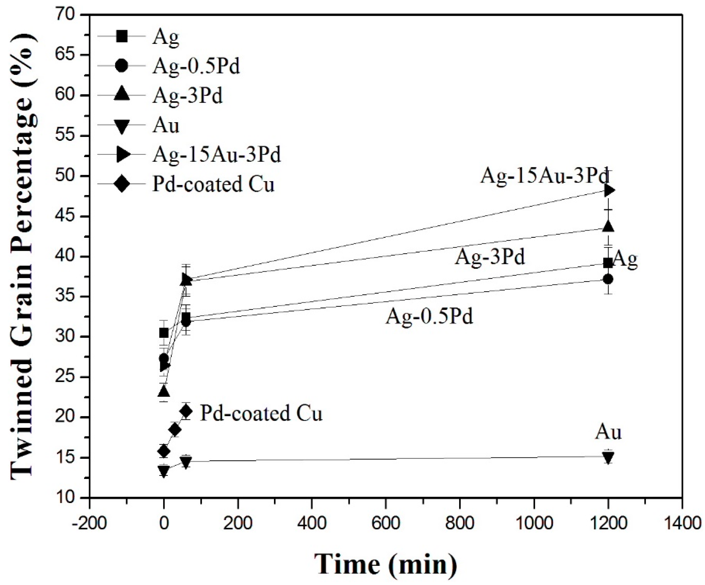
Table 1, it can be found that the grain growth exponents of Ag-alloy and pure Ag wires ranged from 0.19 to 0.28; this range is lower than those of pure Au wire (0.30) and Pd-coated Cu wire (0.38). The results were correlated with the twinned grain percentages in the pure Ag and Ag-alloy wires, which were much higher than those in the conventional Au wire and Pd-coated Cu wire, as shown in
Figure 10. In addition, the similar grain growth exponents of Ag-3Pd and Ag-15Au-3Pd wires imply that the solid solution of Au atoms in Ag matrix has a minor effect on its grain growth kinetics. Furthermore, the pure Ag and near-pure Ag-0.5Pd wires have similar grain growth exponents, which are obviously larger than those of Ag-3Pd and Ag-15Au-3Pd alloy wires. This finding can be attributed to the solute drag effect of 3% Pd element on the grain boundary migration of Ag- and Ag-Au- alloy wires [
22,
23].
The enrichment of annealing twinned grains is attributed to the lower stacking energy after cold working and annealing treatments, as reported by Dillamore et al. [
24]. In addition, the manufacturing method of multiple drawing interspersed with annealing treatments further enhanced the formation of annealing twins [
5]. The abundant twin boundaries with low interfacial energy anchored the high angle grain boundaries, retarding grain growth in these annealing twinned Ag-alloy wires. Furthermore, it is notable in
Figure 10 that the twinned grain percentages in all bonding wires increased with the current stressing. Especially, for the Ag-alloy wires containing various Pd and Au contents, the percentages of annealing twins in the original wire grains—ranging from 23% to 30%—rose to between 37% and 48% after 20 h of stressing. It is obvious that the electron flow can also promote the formation of annealing twins, which inhibit the grain growth. This result seems to be contradictory to the phenomenon that the current stressing can be a driving force for grain growth. This contradiction is explained by the fact that the grains without annealing twins have a higher tendency to recrystallize and grow during current stressing, so the total number of grains decreases. Meanwhile, new twins are created in these recrystallized and grown grains through the electron flow, so the number of twinned grains increases. The two effects combine to increase the twinned grain percentage, as shown in
Figure 10.
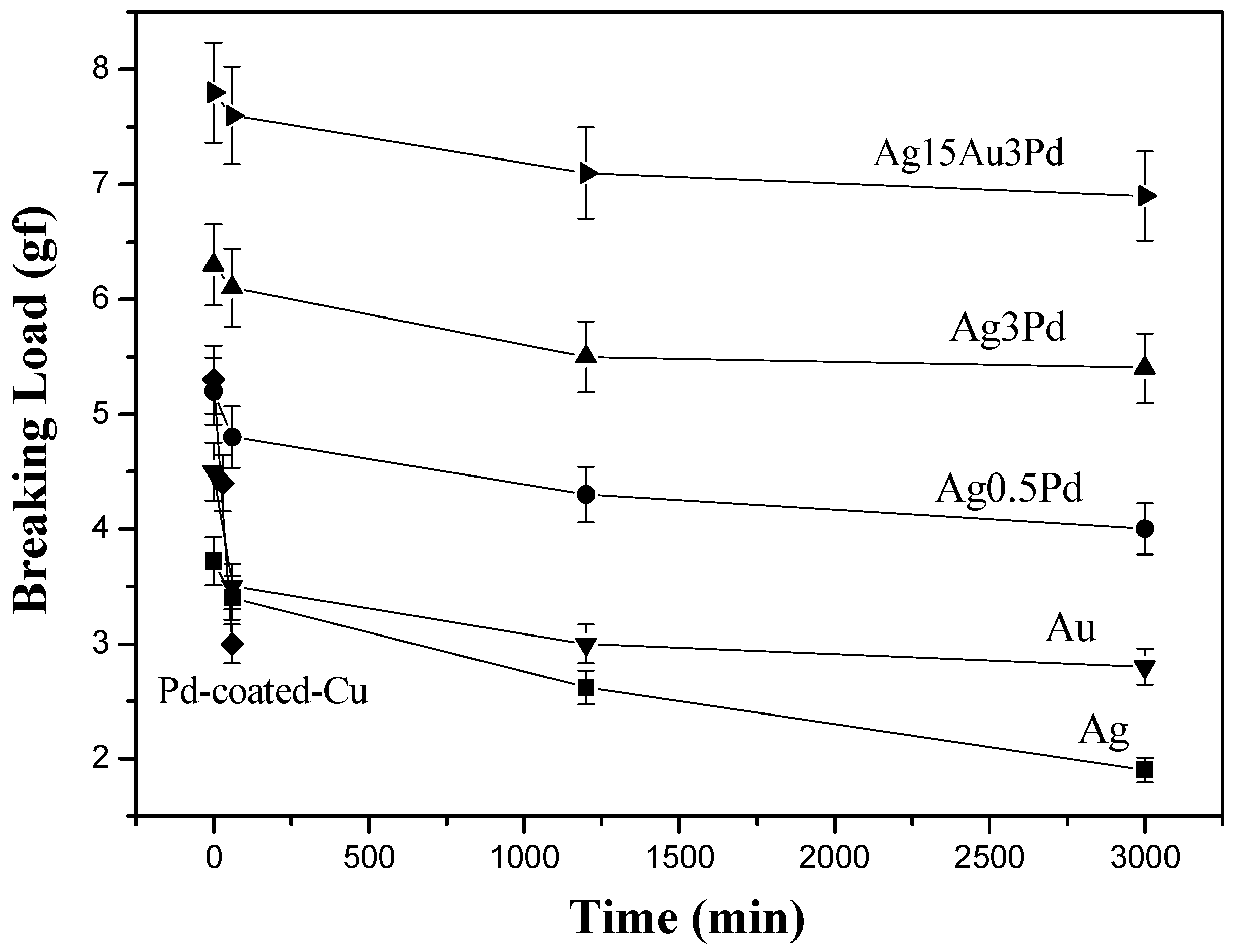
Figure 11 and
Figure 12 show the results of tensile tests of all bonding wires after electrical stressing at 1.23 × 10
5 A/cm
2 for various times. The results in
Figure 11 indicate that the breaking loads decreased with the lengthening of stressing time, which can be attributed to the grain growth in the wires during the current stressing. In addition, the concave notches on the wire surfaces visible in the micrographs of
Figure 2c,
Figure 3c,
Figure 4c,
Figure 5c,
Figure 6c,
Figure 7c were created by the mass transportation during current stressing due to the equilibrium of interfacial energies at the intersection of the grain boundary and the wire surface. These notches can also lower their breaking loads.
Figure 11 also shows that the breaking loads of all of the Ag-alloy wires were higher than those of the pure Au and pure Ag wires under current stressing, with a sequence of Ag-15Au-3Pd > Ag-3Pd > Ag-0.5Pd > Au > Ag. It is obvious that the addition of Pd and Au strengthened the wire materials. In addition, the enrichment of annealing twins in Ag-alloy wires can also increase their breaking loads. Although the original Pd-coated Cu wire had a high breaking load of 5.3 g, it dropped drastically to a low value of 3.0 g after current stressing at 1.23 × 10
5 A/cm
2 for only 1 h due to severe oxidation on its outer surface.
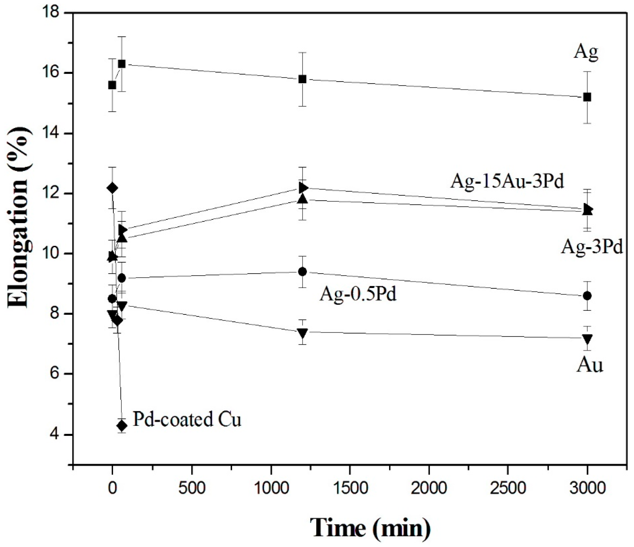
The original pure Ag and Pd-coated Cu wires had very high elongations, 15.6% and 12.2%, respectively. After electrical stressing for 1 h, the elongation of pure Ag wire increased due to the recrystallization and grain growth, as shown in
Figure 12. Although further current stressing decreased its elongation moderately, it was still higher than those of the other wires. In contrast, severe oxidation on the surface of Pd-coated Cu wire reduced its elongation to a low value of 4.3% after only 1 h of current stressing at 1.23 × 10
5 A/cm
2. It is also evidenced in
Figure 12 that the elongations of pure Ag and Ag-alloy wires were higher than that of pure Au wire under electrical stressing, with a sequence of Ag > Ag-15Au-3Pd > Ag-3Pd > Ag-0.5Pd > Au. Similar to that of pure Ag wire, the elongations of pure Au and Ag-alloy wires also increased after initial current stressing for 1 h and then dropped slightly during further stressing. However, the decline was smaller in Ag-alloy wires than in pure Au wire. The surface morphology and mass transportation in Ag-alloy wires after electrical stressing seem to have insignificant influences on the variations in elongation due to the existence of annealing twins.


