Review

Review of Electromagnetic-Based Crack Sensors for Metallic Materials (Recent Research and Future Perspectives)

School of Electrical and Electronics Engineering, Chung-Ang University, 84 Heukseok-ro, Dongjak-gu, Seoul 156-756, Korea
*
Author to whom correspondence should be addressed.
Metals 2016, 6(8), 172; https://doi.org/10.3390/met6080172
Submission received: 20 May 2016 / Revised: 8 July 2016 / Accepted: 20 July 2016 / Published: 25 July 2016

Abstract

:
Evaluation and non-destructive identification of stress-induced cracks or failures in metals is a vital problem in many sensitive environments, including transportation (steel railway tracks, bridges, car wheels, etc.), power plants (steam generator tubing, etc.) and aerospace transportation (landing gear, aircraft fuselages, etc.). There are many traditional non-destructive detection and evaluation techniques; recently, near-field millimeter waves and microwave methods have shown incredible promise for augmenting currently available non-destructive techniques. This article serves as a review of developments made until now on this topic; it provides an overview of microwave scanning techniques for crack detection. This article summarizes the abilities of these methods to identify and evaluate cracks (including describing their different physical properties). These methods include applying filters based on dual-behavior resonators (DBRs), using complementary split-ring resonators (CSRRs) for the perturbation of electric fields, using waveguide probe-loaded CSRRs and using a substrate-integrated-waveguide (SIW) cavity for the detection of sub-millimeter surface and subsurface cracks.

Graphical Abstract

1. Introduction

Failure or metal fatigue usually starts at the outside surface of a metallic object. Nuclear plants, aircraft fuselages, steel bridges and steam generators are examples of applications in which metal fatigue or failure is likely to occur. Therefore, stress and fatigue crack detection is an essential aspect of the thorough evaluation of sensitive metallic structures. There are many well-known non-destructive evaluation (NDE) methods for identifying surface cracks in metals. Eddy current testing, acoustic emission testing, ultrasonic testing, dye penetrant testing, magnetic particle testing and radiographic testing are examples of testing methods [1,2,3,4]. For example, cracks under coatings, such as rust, paint, corrosion protection substances and composite laminates, are not always consistently detected using these techniques. The same concern applies to cracks filled with dielectric materials, such as dirt, paint, rust or other materials. Environmental issues must also be considered when using an NDE method (e.g., contamination resulting from the dye penetration technique). The removal of surface coverings or coatings, in order to simplify crack detection, is a difficult approach. Moreover, remote crack detection is desirable from an experimental and practical point of view.
Before 1993, microwave NDE methods were used for the detection of surface cracks in metals; however, these methods were not fully successful [5,6,7,8]. After 1993, near-field microwave crack detection techniques and approaches that use open-ended waveguide probes were introduced [9,10,11,12,13,14,15,16,17]. Investigations of the application of these methods for the detection and evaluation of fatigue surface cracks showed many unique and advantageous features, such as:
  • The probe need not be in contact with the surface under examination.
  • The methods are applicable in high-temperature environments.
  • Cracks may be filled with dielectric materials, such as dirt, paint or rust.
  • The surface of the metal may be covered with paint or a similar compound, and the crack may still be detected because microwaves penetrate dielectric materials.
  • The methods are applicable to both non-ferromagnetic and ferromagnetic metals or alloys and coarse-grained materials, because microwaves do not penetrate metal and depend on perturbations in the surface current.
  • The dimensions of a crack can be accurately estimated.
  • The polarization properties of microwaves can provide information regarding relative crack orientation.
  • Crack tip location can be determined.
A broad depiction of near-field microwave methodologies and techniques using open-ended waveguide probes established in the early 1990s for evaluating and detecting cracks is addressed in [17]. These methodologies were extended and used for detecting V-shaped [18] and tilted [19] cracks. Furthermore, numerical analysis was carried out to facilitate a statistical quantitative approach for multiple probes to repetitively detect a crack and differentiating it from other irregularities [20,21]. A near-field technique using open-ended coaxial probes was also reported in the literature [22,23,24,25]. This technique features numerous distinctive advantages, including the ability to analyze cracks near edges, rivets, corners and tight places and inside bore holes, because the coaxial probe is made up of semi-rigid coaxial lines, which can be easily bent. Recently, imaging of the actual cracked metal slabs for improved crack detection sensitivity has also been demonstrated at the lower millimeter wave frequencies (less than 100 GHz) [26]. This article reviews established scanning methodologies exclusively designed for crack evaluation and detection. These methods include open-ended rectangular probes, open-ended coaxial probes, filters using dual-behavior resonators (DBRs), a substrate-integrated-waveguide (SIW) cavity and a complementary split-ring resonator (CSRR).

2. Background

The well-established traditional microwave range is from 300 MHz to 30 GHz, whereas the frequency range of 30 GHz–300 GHz is referred to as the millimeter wave spectrum; the corresponding wavelength ranges are 1000–10 mm and 10–1 mm, respectively [27]. At these frequencies, signals do not pass through metal surfaces; however, they are responsive to the existence of hard metallic incoherence, such as roughness or cracks. However, at these frequencies, signals penetrate through dielectric materials (such as dirt or paint) and, therefore, can be used to examine painted metallic structures to detect cracks. In imaging procedures, when operating in the near-field region of open-ended probes, probe dimensions determine the spatial resolution, which tends to be comparatively small at these frequencies. Figure 1 shows the top view of the apertures and flanges of standard open-ended waveguides for several different frequency bands, including the K-band (18–26.5 GHz) with an aperture dimension of 10.7 mm by 4.3 mm, the Ka-band (26.5–40 GHz) with an aperture dimension of 7.11 mm by 3.56 mm, the V-band (50–75 GHz), with an aperture dimension of 3.8 mm by 1.9 mm and the W-band (75–110 GHz) with an aperture dimension of 2.54 mm by 1.27 mm. Open-ended coaxial probes can function over an even wider frequency range for a given probe geometry. Detecting a crack with an open-ended waveguide or a coaxial probe at the near-field region is achieved by perturbing the current on the surface of the metal. When using these probes for the detection of cracks, the perturbation of the induced surface current density on the metal plate caused by the presence of a crack allows detection and extracts important data about its physical geometry. This is a sensitive function of the crack dimensions and placement within the probe space. Therefore, to detect a crack on the surface, relatively low frequencies can be helpful for detecting tight cracks (e.g., cracks with an approximately 5-μm opening have been detected at frequencies near 10 GHz, a crack-width to wavelength ratio of approximately 0.00016) [23,25]. When using an open-ended waveguide probe, a surface current is generated on the metal surface under investigation, thereby creating a reflected wave and, subsequently, a standing wave inside the probing waveguide. The presence of a crack inside the waveguide space disrupts the current density and changes the properties of the standing wave or reflected wave. Note that the current density does not depend significantly on the kind of metal in crack detection applications, because all metals are treated as perfect conductors [27]. Probing the standing wave shape inside the waveguide, as a cracked surface is scanned, provides important data regarding the existence of the crack. Furthermore, the ability of signals to penetrate dielectric materials enables the non-destructive detection of surface cracks that are intentionally covered with dielectric coatings, such as corrosion-protecting materials, laminate or paint, and/or are accidentally covered with dielectric materials, such as rust, paint or dirt. Finally, the physical properties of the change in the reflected wave provide useful data regarding the location and geometry of the crack(s) within the open-ended probe space.

3. Band-Pass Filters Based on DBRs

This section gives a detailed explanation of how micro-cracks can be detected and imaged at the surface of metals using a near-field RF (radio frequency) method from the crack-triggered changes in resonant frequency and the resonant circuit QF (quality factor). As described in the literature [29], there are two sensors: a quarter-wavelength microstrip-line resonator, followed by an electric dipole and an innovative DBR band-pass filter probe. The phenomenon of detection is produced primarily using probing of the electric dipole. The low sensitivity of the electric dipole resonator caused the authors to examine whether first-order band-pass filters based on dual-behavior resonators were able to detect a 3-mm-deep and 200-μm-wide rectangular crack at the steel surface used to authenticate their method. Simulation data and measurements results from a fake steel sample with many 200-μm-wide rectangular notches showed that the DBR sensor is more accurate and robust to changes than the probe containing an electric dipole and emphasized the connection between the spatial resolution and the width of the high-frequency stub of the DBR filter. Furthermore, they validated crack detection for any position of the imperfection in accordance with the DBR sensor and the capability to distinguish amongst cracks with altered depths. Simulation data and measurement results were presented and discussed.

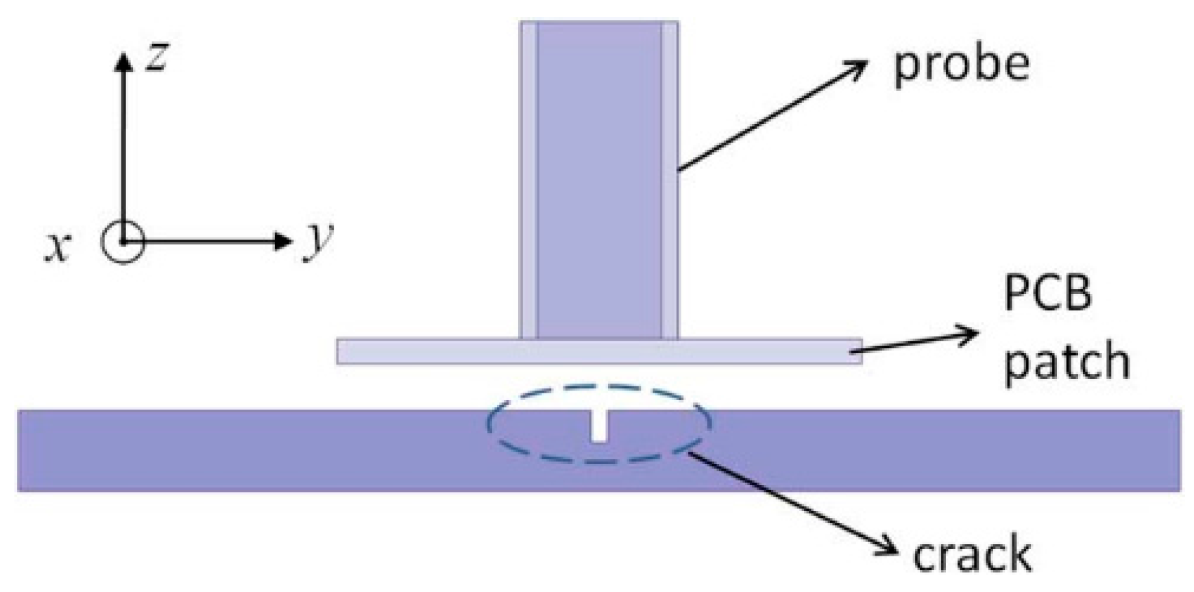
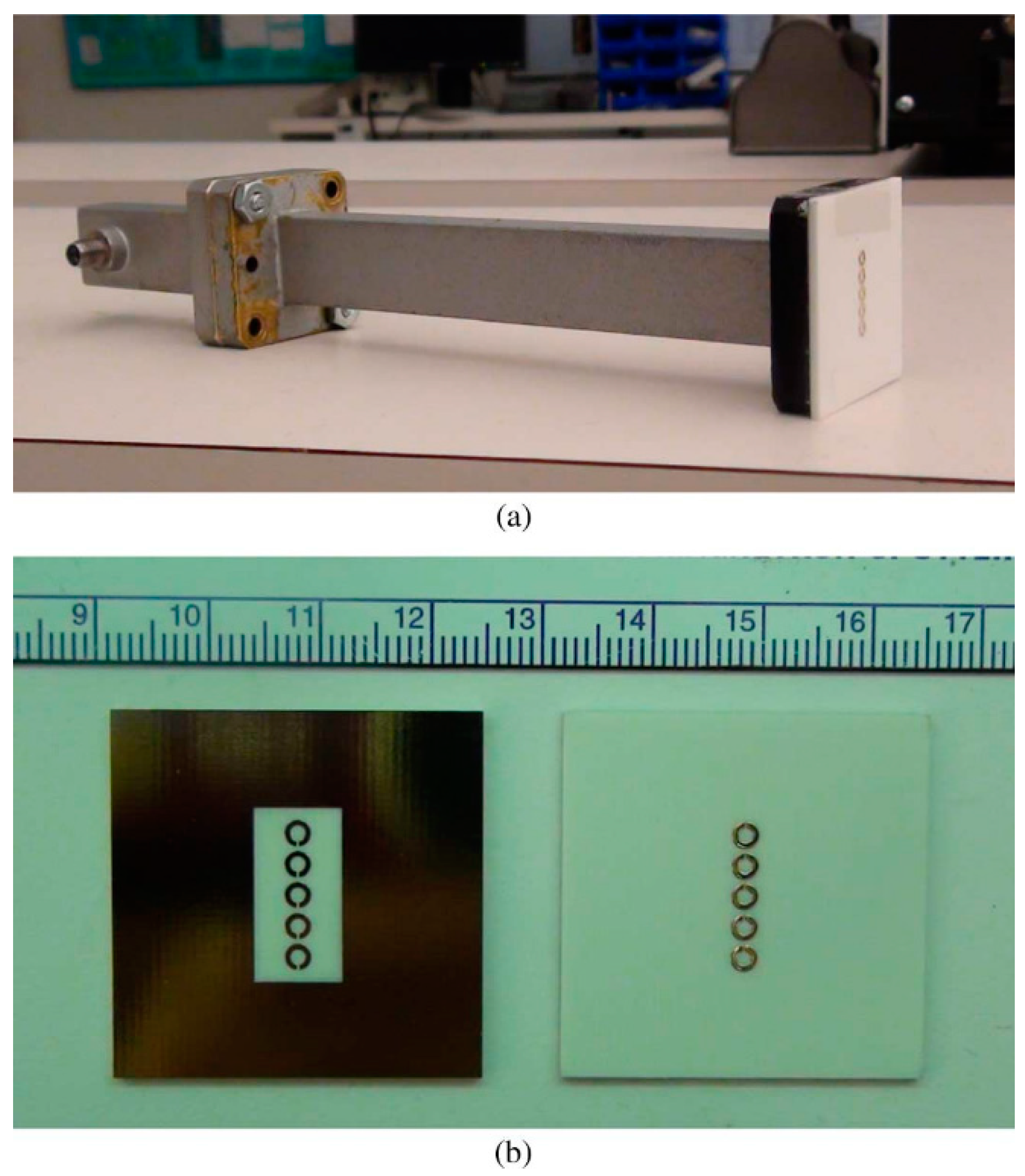
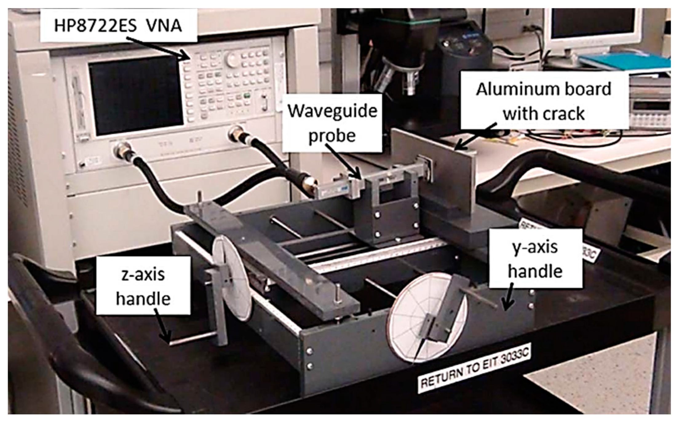
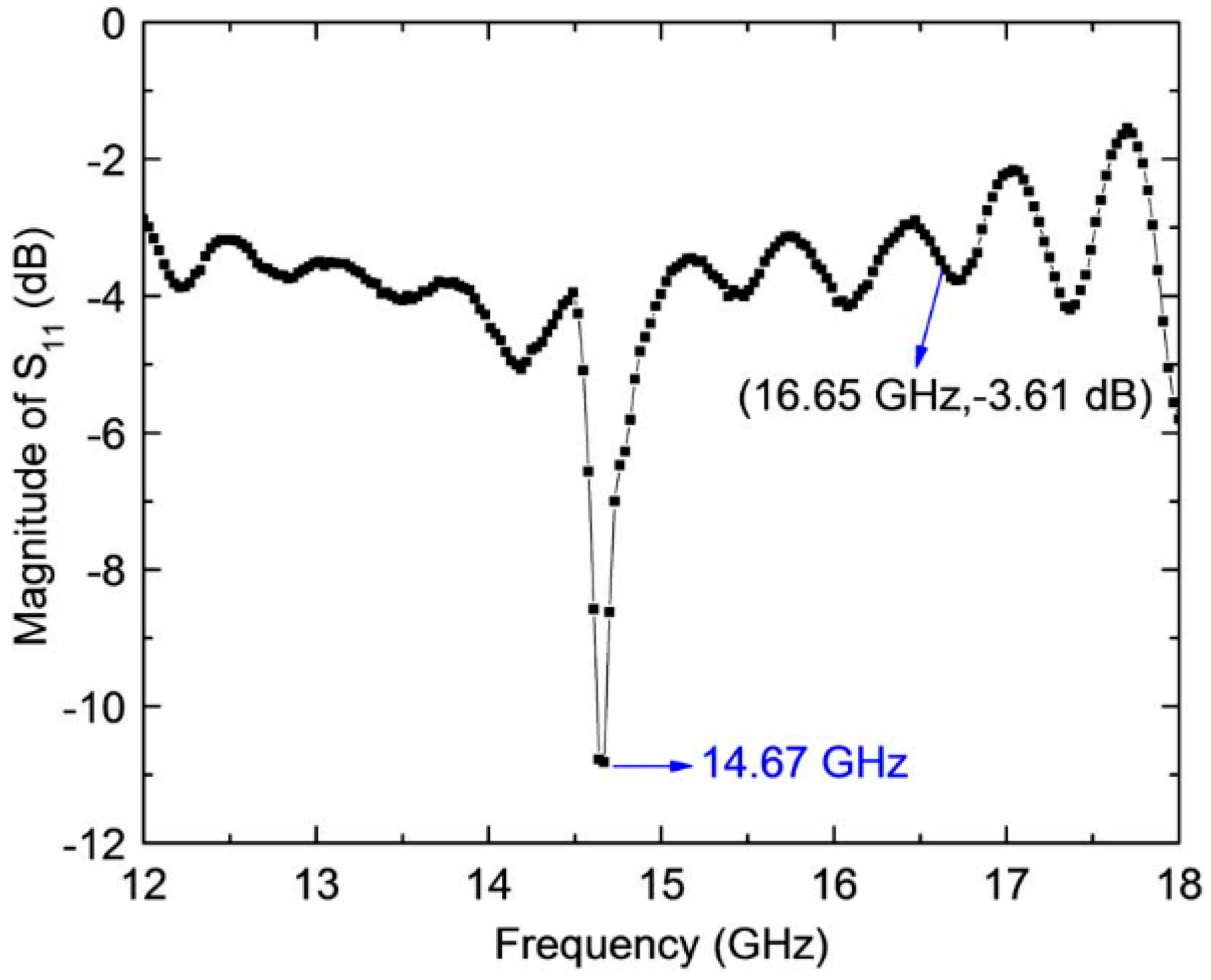
3.1. Feasibility and Relevance of Crack Detection Using an Available Microwave-Based Technique

To place the suggested device in the viewpoint, the authors examined how accurately the microstrip electric dipole probe developed by Tabib Azar et al. [30] can sense a 3-mm-deep and 200-μm-wide crack at the exterior of an austenitic steel plate. Simulations with high-frequency field simulation software (HFSS) and measurements were intended to estimate the sensor’s resolution and sensitivity. The DBR filter sensor and the electric dipole probe were constructed on an alumina substrate, and the geometry was chosen to attain a resonant frequency of approximately 10 GHz. This setup permits one to work with compact circuits and to find resonant frequency changes that can be conveniently measured using a VNA (vector network analyzer). The suggested applicability of the magnetic dipole probe proposed by Tabib-Azar [30,31] was also evaluated.
Figure 2 shows the construction of the electric dipole probe, consisting of a quarter-wavelength-long microstrip line over an alumina substrate followed by a radiating electric dipole [30]. The substrate (25.4 × 25.4 mm) is made of 508-μm-thick alumina (permittivity εr = 9.4, and loss tangent tan δ = 6 × 10⁻³). The transmission lines on the alumina substrate are made of gold (conductivity σ = 4.1 × 10⁷ Sm−1) with a thickness of t = 5 μm. The radiating electric dipole is made up of two gold wires (17 μm in diameter) soldered to the taper end such that the radiation produced from the resonator is focused on the metal section. To confirm the accuracy of simulation data, measurements were performed on a steel surface with several 200-μm-wide cracks. The experimental arrangement is presented in Figure 3, which shows an Agilent PNA E8364A (45 MHz–50 GHz) network analyzer and a motorized three-axis displacement device holding the probe. Figure 4 shows a representation of the probe over a crack. The width (W, x direction), depth (h, z direction) and length (L, y direction) of the notch under study are 0.2, 3 and 10 mm, respectively. Figure 5 shows the progress versus frequency of the reflection coefficient (S11) when the probe was set above a faultless metal plate and above the middle of the 200-μm-wide notch. The observed shifts are ∆fr = 10 MHz and ∆Q = 80 (∆Q/Q = 17.3%) [28]. Figure 6 shows the variations of the resonance frequency ∆fr when a 1D scan is performed along the x direction for probe-to-metal distances d of 50 and 75 μm. The probe step increment is 10 μm; the origin (x = 0) corresponds to the middle of the notch. Figure 6 shows that the sensitivity is better for d = 50 μm; in this case, the variation ∆fr between the middle of the notch and the faultless metal is 10 MHz, versus 4.5 MHz for d = 75 μm.
The microstrip dipole probe clearly shows its ability to sense micro-cracks on the surface; however, the measurement setup confirms the subsequent disadvantages: for the researcher, positioning the two dipole wires to be precisely collinear and exactly observing the distance between them both proved to be very difficult. Consequently, using probes in research laboratory tests may not be the same situation as the final version analyzed in simulations. Furthermore, as the wires are delicate and carefully bent, they can be damaged by mishaps. Finally, because the fr and Q changes produced by the faults are comparatively minor, it might be necessary to use a sensor that is more sensitive.

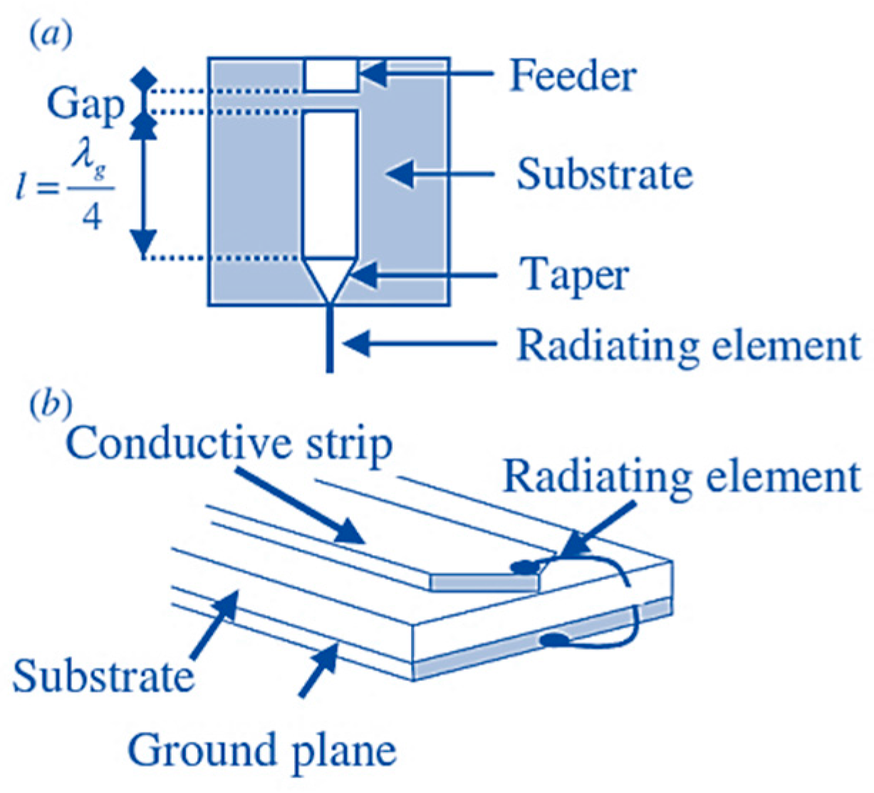
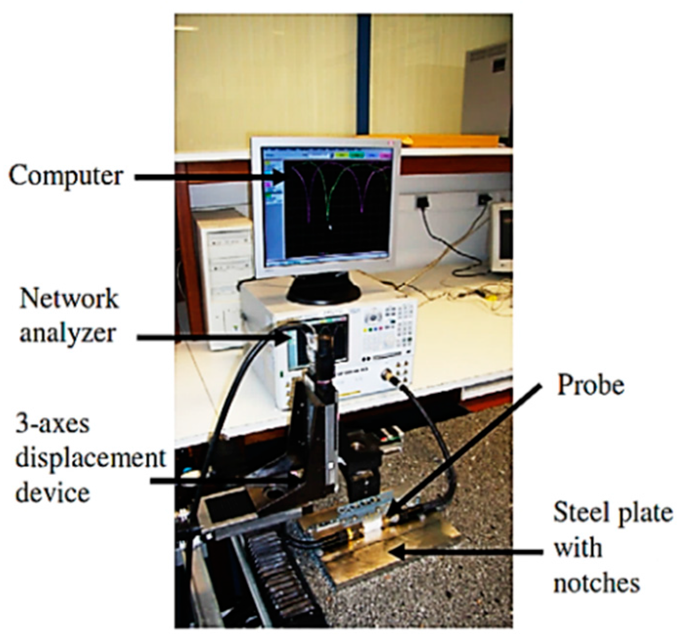
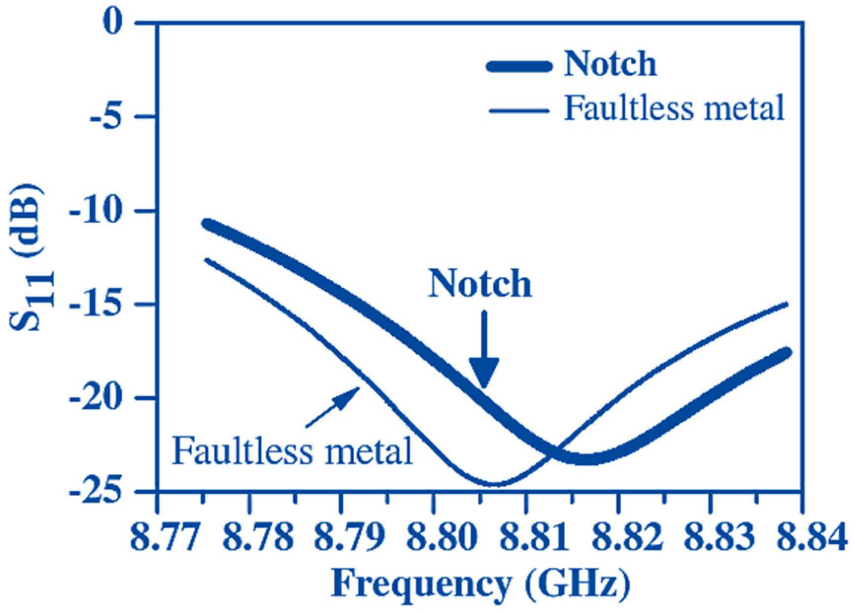
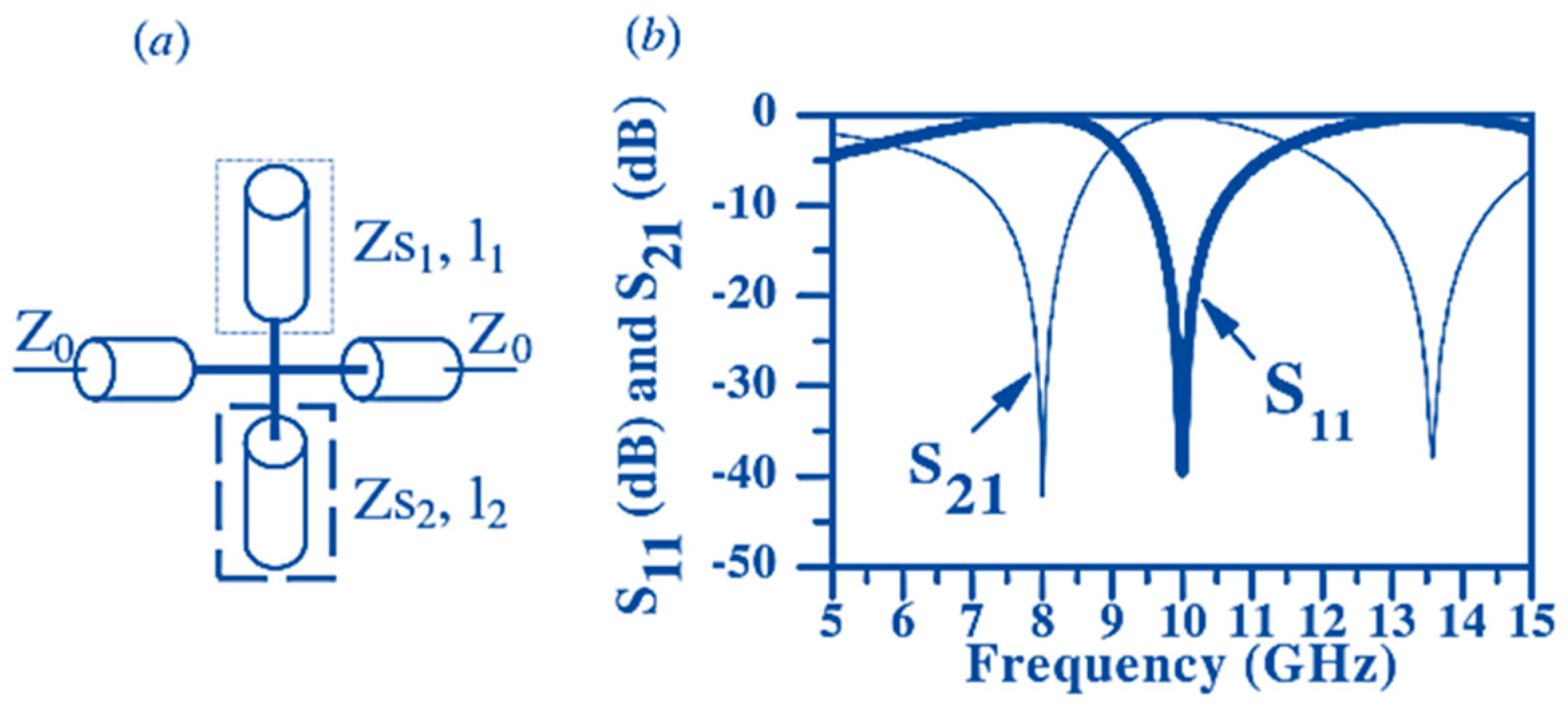
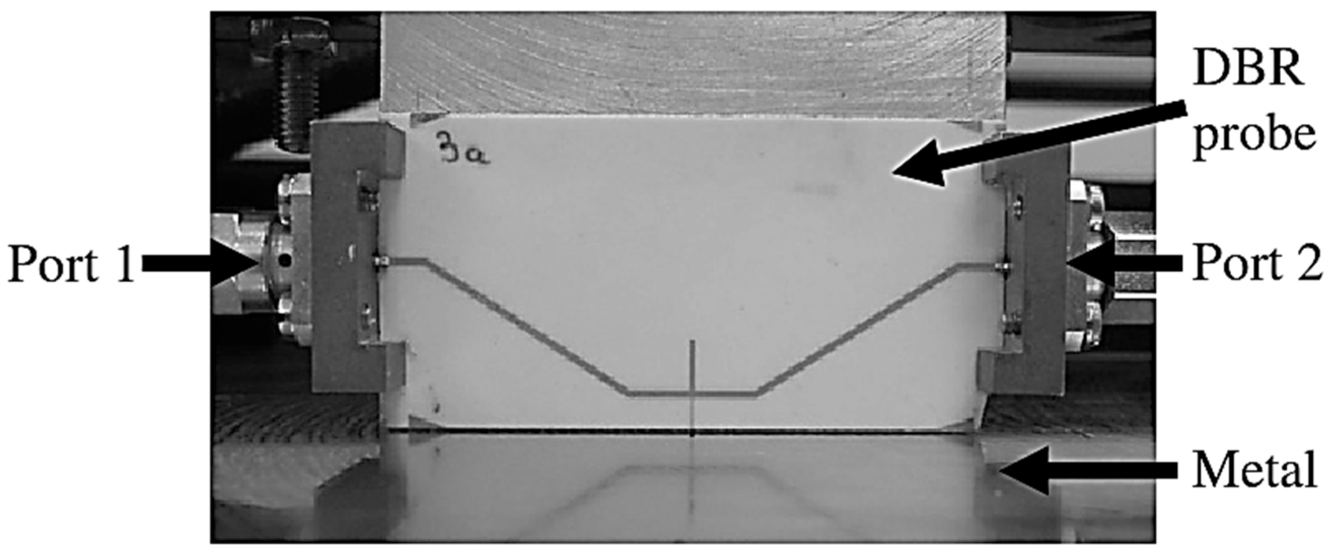
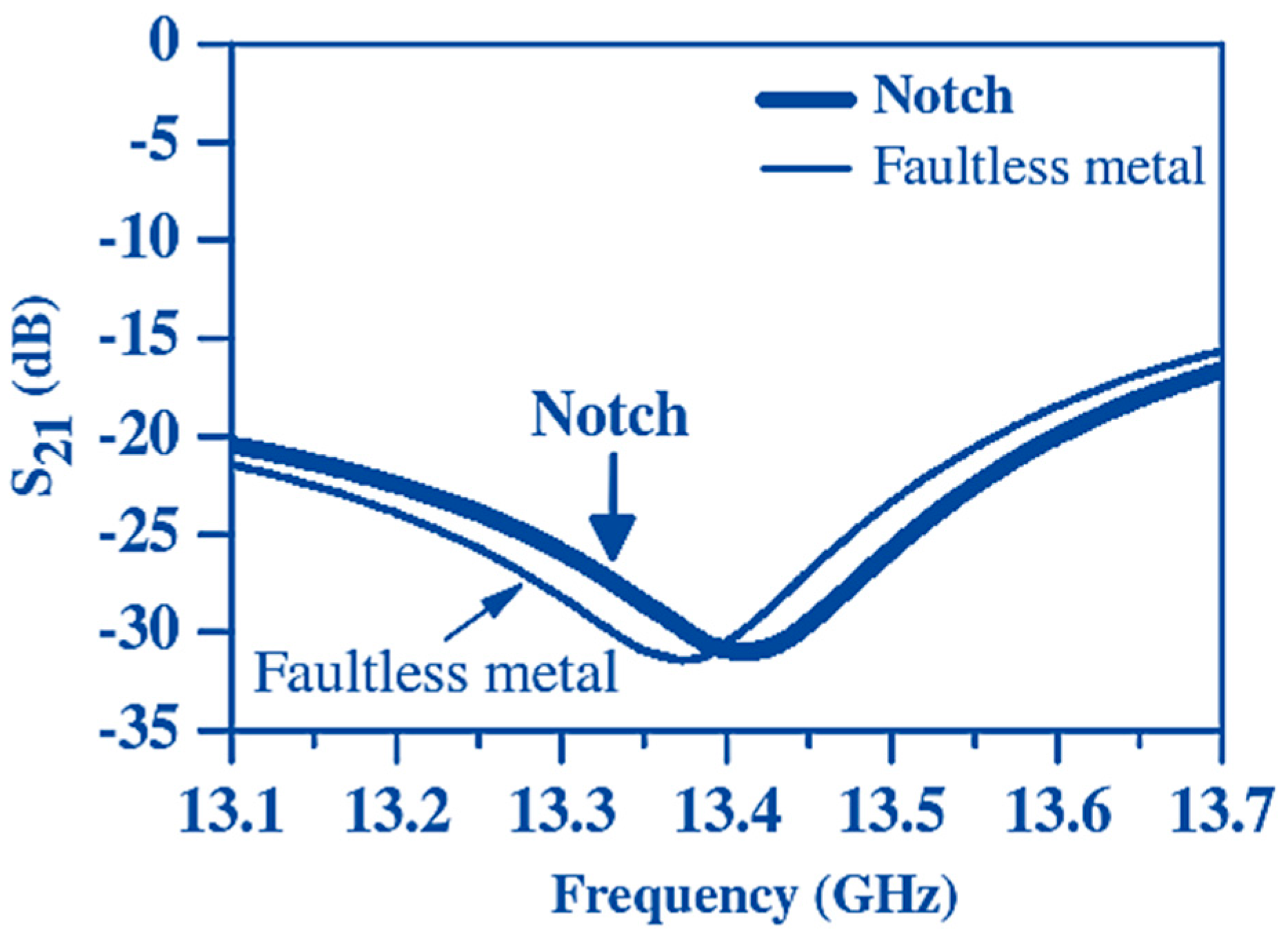
3.2. DBR Filter Probe

To improve sensitivity, the authors of this work chose the DBR arrangement to apply the transmission and reflection properties of the band-pass filter (BPF). The DBR filter allows free control of the transmission zeros associated with the high- and low-attenuated bands with increased QFs. A DBR resonator is created using the combination of two dissimilar parallel band-stop configurations [32,33]. Each of these configurations has its own transmission zero based on its dominant resonance criteria. The novelty of this DBR filter is proven here, because it tolerates independent control of its tuning parameters: The researcher can assign a location to the first transmission zero independently of the second transmission zero.
Figure 7a illustrates the design, and Figure 7b presents the reflection (S11) and transmission (S21) parameters of this first-order DBR BPF, constructed on an alumina substrate. The phenomenon of detecting micro-cracks consists of measuring variations in the capacitive coupling between the HF stub (of width W) accompanying the filter’s upper attenuated band and the metal surface. The interaction between the metal plate and the HF stub (which are separated by a distance d) artificially spreads the distance of the latter and drops the transmission zero frequency in the upper attenuated band. The literature on near-field microscopy shows that the spatial resolution of an evanescent probe is governed by the size of the probe end (WHF for the DBR filter) and the probe-to-sample distance d [34,35,36,37]. According to [37], the conditions required to resolve a defect of width W are WHFW and dW. Because the purpose of this research is to detect 200-μm-wide surface cracks, it seems pertinent to create two DBR filters with WHF = 50 μm and W = 100 μm. Additionally, the substrate was cut out at the HF stub end to reinforce the radiated electromagnetic field. This phenomenon also augments the coupling between the HF stub and the metal plate. Figure 8 and Figure 9 present a schematic and a photograph of the first-order DBR device used for the detection of micro-cracks on surfaces.
To obtain additional awareness of the relations of a first-order DBR filter with faultless metal and metal with a 200-μm-wide surface crack, simulations were performed using HFSS. The simulation data for the 100-μm-wide HF stub filter set at d = 50 μm above the steel plate indicates increases in fHF and f0 of 98 and 32 MHz, respectively (data not shown), when the probe is above the center of the crack. Furthermore, the crack decreases the QF of the DBR filter sensor (Q = 42.841 versus Qfaultless = 48.963, i.e., ∆Q/Q = 12.5%).
Measurements were carried out using the same settings (Figure 3) and the same crack parameters (W = 0.2 mm, h = 3 mm and L = 10 mm) as in the data using the electric dipole. Two first-order DBR filters with different HF stub widths were studied (Filter 1: WHF = 100 μm; Filter 2: WHF = 50 µm). Figure 10 shows the transmission parameter responses obtained using the 100-μm-wide high-frequency stub filter for a probe-to-sample distance of 50 μm. The existence of the cut causes an increase in fHF (∆fHF = 39 MHz) and f0 = 15 MHz (data not shown) and a decrease in the QF (Qnotch = 44.741 versus Qfaultless = 46.165, i.e., ∆Q/Q = 3.1%). Figure 11 shows the differences in ∆fr obtained for the two DBR filters when a 1D scan was performed in the x direction with a 10-μm probe increasing step and d = 50 μm. This figure shows that ∆fr is the highest in the middle of the notch (∆fr = 39 MHz for Filter 1; ∆fr = 51 MHz for Filter 2) and that the 50-μm-wide high-frequency stub filter is more robust than the 100-μm-wide high-frequency stub filter. These measurement results are in very close agreement with the simulation results carried out using HFSS, which show, for a probe-to-metal distance d = 50 μm, that the diameters of the metal surfaces illuminated by the 100- and 50-μm-wide high-frequency stub filters are approximately 350 and 200 μm, respectively. Additionally, the corresponding x value for the electric dipole is 180 μm; its spatial resolution is somewhat enhanced relative to the spatial resolution of the DBR filter with the 50-μm-wide high-frequency stub. Nevertheless, the sensitivity is significantly improved by the DBR filter [29].
The authors have shown [29], experimentally and theoretically, that a resonant near-field probe can sense a surface crack in a metallic surface. The idea was initially authenticated using research into the microstrip electric dipole resonator developed by Tabib-Azar et al. Experiments conducted for the 3-mm-deep and 200-μm-wide rectangular cracks were utilized to confirm their method; results emphasized the high spatial resolution of the electric dipole probe, but they also showed its crumbliness and low sensitivity. To avoid these two disadvantages, the authors [29] replaced the electric dipole probe with a novel first-order DBR BPF sensor. The scans performed above the 3-mm-deep and 200-μm-wide cracks showed (i) a significant improvement in the sensitivity when using the first-order DBR arrangement, (ii) a connection between the spatial resolution and the width of the high-frequency stub of the DBR filter and (iii) the likelihood of sensing and imaging the crack for any dimension based on the DBR sensor. DBR probes can also be used for sensing faults and non-uniformities in several materials and for identifying corrosion under paint.

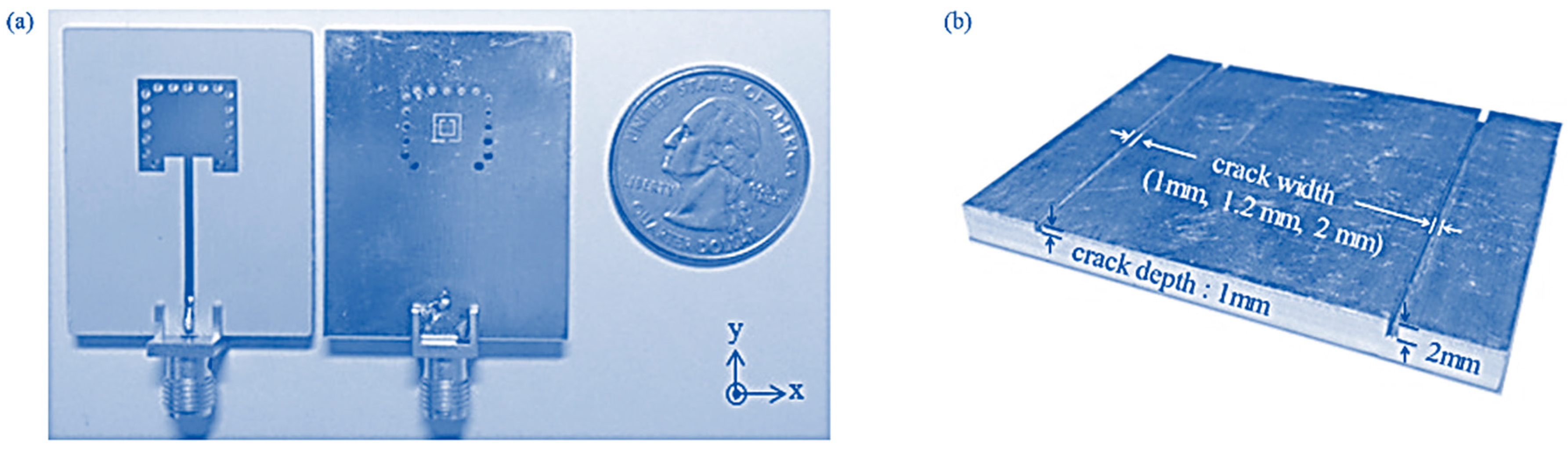
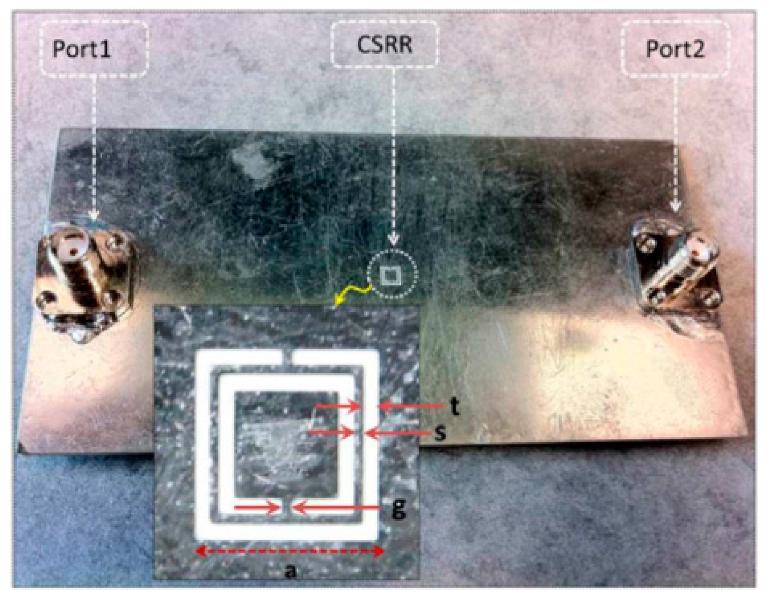
4. CSRR for Crack Detection in Metallic Surfaces

In this section, a new sensor based on a CSRR is presented to detect sub-millimeter surface cracks. The sensing mechanism is based on perturbing the electromagnetic field around an electrically small resonator, thus initiating a shift in the resonance frequency. The sensor is simple to fabricate and inexpensive, as it is etched in the ground plane of a microstrip-line using printed circuit board (PCB) technology. The sensor exhibits a frequency shift of more than 240 MHz for a 100-μm crack [38]. In essence, the CSRR is used as a near-field sensor for crack detection. The effectiveness of the sensor is demonstrated experimentally. The advantages of the CSRR sensor, as compared to the other microwave techniques for crack detection, are lower operating frequency, higher sensitivity and relatively low fabrication cost.
In this work, the authors used a single CSRR as a sensing element to detect sub-millimeter-sized cracks in metallic surfaces. The objective was to design the sensor to operate near 5 GHz. This value was based on the availability of relatively inexpensive microwave components. The eigenvalue solver of Ansoft HFSS was used to achieve a CSRR with dimensions of a = 3 mm and s = g = t = 0.2 mm. Because of the fabrication limitations and milling machine tolerances, the final fabricated sensor had dimensions of a = 3 mm, s = 0.27 mm and g = s = 0.16 mm, as shown in Figure 12. We emphasize, however, that our objective in designing the sensor is to achieve a resonance frequency close to 5 GHz. Achieving resonance at a specific frequency is of minor importance here.
The CSRR sensor is agitated using an electric field that is perpendicular to the exterior of the sensor in a way equivalent to that using a split-ring resonator arrangement, for which a magnetic field is required for excitation. Consequently, a microstrip line (MSL) structure is selected for exciting the CSRR (the microstrip line can be treated as a feeding mechanism for the sensor). The CSRR is etched in the ground plane of the microstrip. A diagram of the sensor structure is shown in Figure 13. The transmission parameter is measured using a VNA. The MSL is designed in order to compensate for the internal impedance of the network analyzer, as in the experimental setup. Alternatively, the MSL can be constructed to compensate for the internal impedance of any other possible feeding device. For a characteristic impedance of 50 Ω, the width of the MSL is kept at 1.68 mm, based on a Rogers RO4350 substrate (thickness = 0.75 mm, relative permittivity = 3.48 and loss tangent of 0.0031). To cover the aluminum plate surface, a thin Teflon film with a thickness of 0.0762 mm is used, which simulates paint or a dielectric coating that can obscure the crack from visual inspection. Once the CSRR is constructed to function at the frequency of interest, the resonant frequency is then noted for the reference case, which is defined as the agreement when the sensor is located directly above a solid aluminum plate bereft of any cracks or defects. The scanning or detection of a crack is completed by sliding the sensor above the aluminum metallic plate, as shown in Figure 13. When a crack is below the sensor, a variation in the resonant frequency of the CSRR is recorded. The sensitivity of the sensor is regulated by both the aptitude used to identify a crack with specific geometry and the change in the resonant frequency from the reference case.
The measurement procedure is also shown in Figure 13. A Teflon-covered aluminum plate is positioned below the sensor. Two cracks measuring 100 μm and 200 μm in width were produced in the aluminum surface. Two dissimilar crack depths of 1 and 2 mm were created for each crack width. The sensor scans the aluminum plate; the transmission parameters are noted when the sensor passes over the cracks and when there is no crack under the sensor. Figure 14 shows the frequency of minimum transmission when the sensor passes over a crack with a width and depth of 100 μm and 1 mm, respectively. A variation in frequency of more than 240 MHz was realized relative to the case without the crack. Figure 15 shows that a 200-μm-wide and 1-mm-deep crack results in a frequency change of more than 260 MHz, consistent with an approximately 5% change relative to the case without the crack.
There is a somehow similar technique also mentioned in [39]. Relative to the other microwave approaches in the literature, the proposed sensor here functions at a lower frequency, has significantly higher sensitivity and is relatively cost effective.

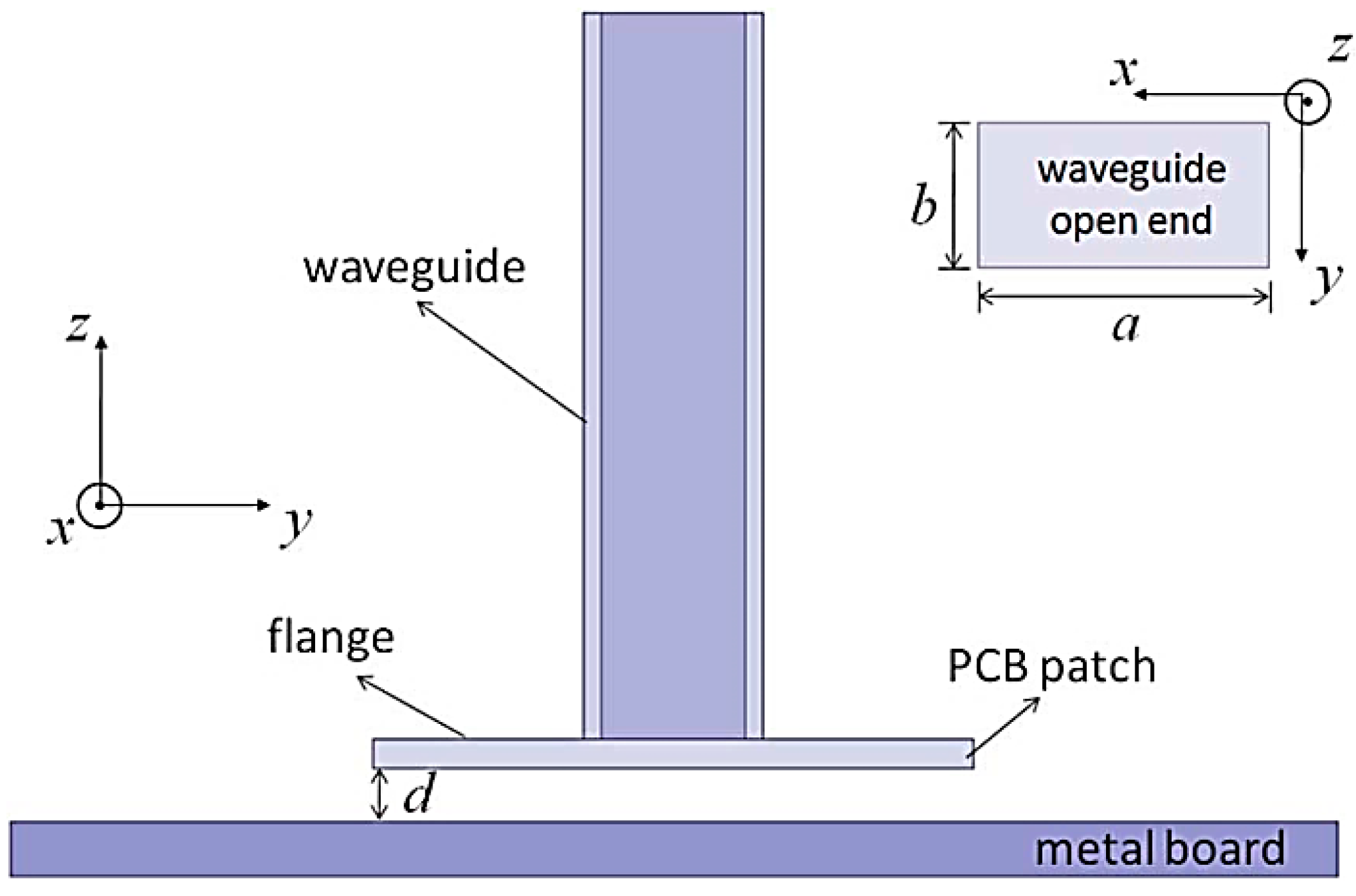
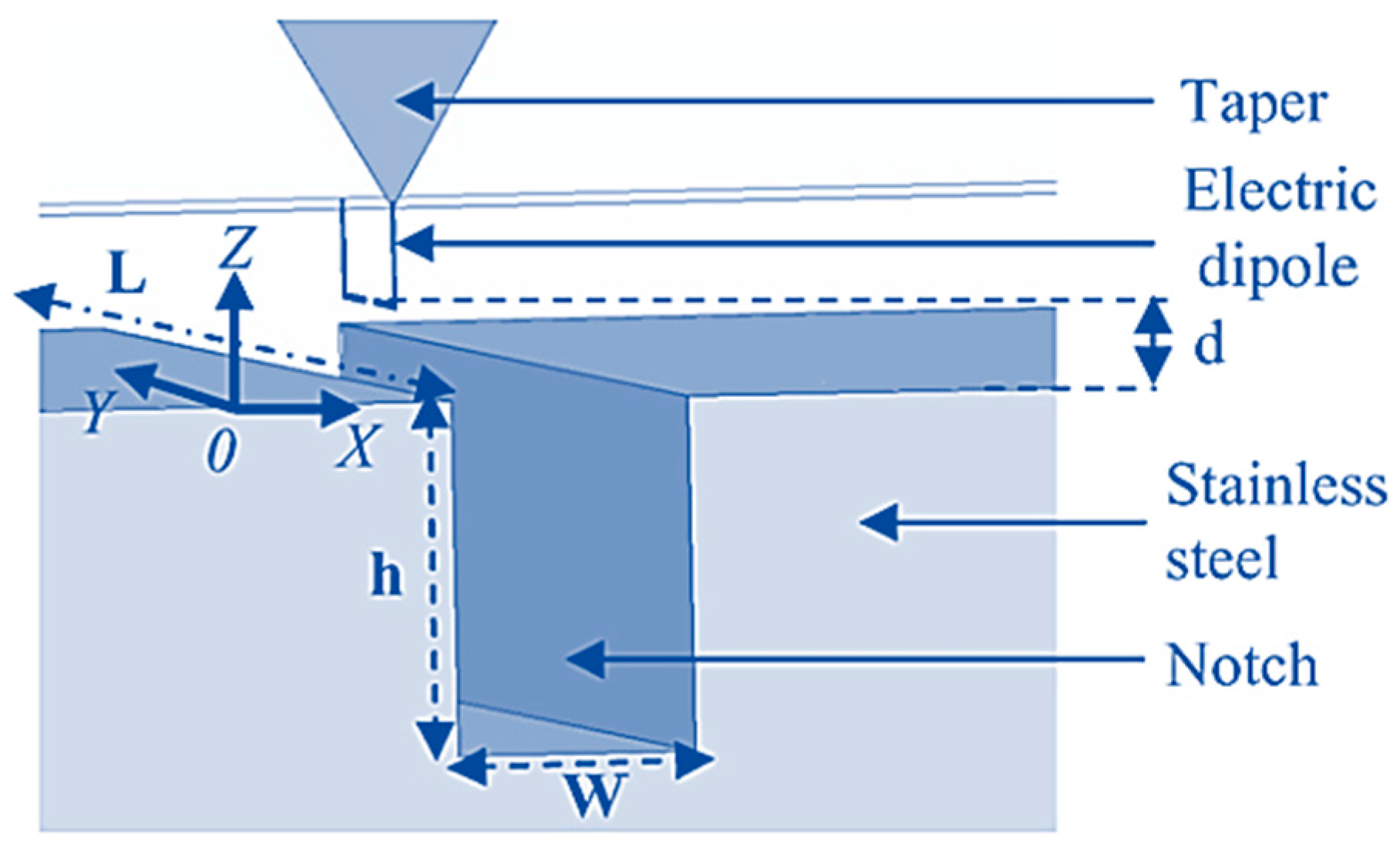
5. Waveguide Probe Using Split-Ring Resonators for Crack Detection in Metallic Surfaces

In this section, a near-field waveguide probe with an embedded array of split-ring resonators (SRRs) that resonate at 16.65 GHz is presented. When the probe scans a surface, the magnetic flux produced from the currents on the metallic surface strongly disturbs the equivalent lumped factors of the SRRs. This, in turn, disturbs the reflection parameter of the feeding port, which leads to high sensitivity in the detection of irregularities, such as cracks in the exterior. Measurement data indicate the possibility of detecting cracks as small as 25 μm in width in metallic surfaces. Furthermore, the probe achieves good resolution in the detection of narrowly-spaced cracks. The authors employed a linear array of circular SRRs to propose a resonant near-field probe. The magnetic field factor perpendicular to the plane of the waveguide opening is used as the exciting field for the SRR cells. A WR-62 waveguide is used. The SRRs are constructed using PCB methods. In the resonant state, the SRR array increases the magnetic field in the vicinity of the waveguide opening, thereby making it appropriate for sensing variations that disturb the resonance state.
When the metal exterior has an extended and trivial crack, the equivalent electrical current on the surface varies. The modification in the current distribution disturbs the magnetic flux in the ring area. To validate this phenomenon, the authors show the current distribution in Figure 16. In this example, the radius of the ring is 20 mm, and the cross-section is a square with dimension of 1 mm × 1 mm. The characteristic impedance of the feeding transmission line is 50 Ω. This ring was intended to resonate at approximately 5 GHz. The resonant frequency of the ring probe is the frequency that resembles the minimum reflection coefficient when the ring is positioned above a metal surface, as will be described below. The distance between the aluminum board and the loop is 5 mm. The width and depth of the crack are 5 and 10 mm, respectively. Figure 16 shows that the distribution of the current is symmetric with respect to x- and y-directed axes centered at the center of the crack. As a result, the currents on the vertical strip surfaces of the crack provide opposite contributions to the magnetic flux in the loop area. The current on the bottom strip surface of the crack provides the same indication, but less flux, because the strip’s surface is farther from the loop than the currents on the surface. Consequently, the flux from the defective metal surface is reduced. The capacitance, conversely, remains almost unchanged because only the overlapping parts of the loop and crack change. Thus, as an effect of the existence of the crack in the metal’s surface, the resonant frequency of the probe shifts to a lower frequency.
Figure 17 indicates the variations in the resonant frequency for the loop above an aluminum board with and without a crack. Figure 17 shows that 4.70 and 4.85 GHz are the resonant frequencies, when the depth of the crack is 5 or 10 mm, respectively. Four-point-nine-five giga-Hertz is the resonant frequency of the loop probe corresponding to an ideal surface. The geometry and presence of the crack modify the magnitude of the reflection parameter. Both the dissimilarity in the reflection parameter magnitude at the resonant frequency and the shift in the resonant frequency can be used as methods for finding cracks in the metal’s exterior. Figure 18 shows the illustration of the waveguide probe with a metal plate in which a crack is to be detected. The probe is located at a fixed distance, with the waveguide flange parallel to the metal surface. The metal panel is scanned by moving the probe over the metal surface, and the reflection coefficient is noted by a VNA. Figure 19 presents the construction of the SRR cell, which is composed of two parallel concentric rings with gaps on opposite sides. This SRR structure is commonly referred to as a broadside-coupled spit-ring resonator (BC-SRR) [39]. The rings are separated by a substrate made of Rogers Duroid 4003 (relative permittivity = 3.38, loss tangent = 0.0027) at the frequency of interest. To analyze the performance of SRR cell and to determine its resonance frequency, the eigenvalue solver of the HFSS is used. For the eigenvalue simulation, the boundaries of the simulation box were positioned at a distance equal to twice the largest dimension of the SRR cell. Figure 19 shows that the radiation condition was essential to the boundaries in the x-y planes and the boundaries in the x-z planes, whereas the periodic boundary condition was applied on the boundaries in the y-z planes. A metal plane (in the simulations, assumed to be a perfect conductor) is positioned next to the resonator with a standoff distance of 0.6 mm. Two resonances are detected for the SRR cells at 14.53 and 16.24 GHz, respectively. Note that these resonance modes are linked to the SRR cells in the presence of the metal surface (in the case of the SRR cells placed in free space, both rings would likely resonate at a single frequency). Figure 20 displays the simulated magnetic field distribution at the rings of the resonator. At the first resonance, the magnetic field is concentrated at the ring that is farther from the metal surface, whereas the second resonance is concentrated at the ring that is closer to the surface. Because the second resonance is predicted to be more sensitive to changes in the metal plate, it is selected as the dominant operating waveguide probe. However, note that this resonance frequency (the second mode) will slightly shift when an array of SRR cells is used, instead of only one.
Typically, defects on the metal surfaces are very fine pits, tiny cracks, or rust. Figure 21 displays the detection plan of the planned probe with a defective metal surface. The operation frequency for the probe is selected as the frequency at which the magnitude of the reflection coefficient undergoes its largest change. To locate this frequency, the resonant waveguide probe with an aluminum plate was simulated. Figure 22 shows the response of the probe with and without a fine crack on the aluminum surface. Figure 22 shows that all of the resonant points shift to lower frequencies when the crack exists. The maximum frequency change is 500 MHz, which was observed at approximately 17.0 GHz. Thus, the change in the magnitude of S11 is very large at this frequency. The magnitude of S11 is 17.73 dB when the aluminum board has a fine crack and is −5.97 dB when the sheet has no crack. Figure 23a shows the fabricated probe using the geometry presented in Figure 19. The measurement setup is shown in Figure 24. The probe is fixed on the y-z platform. The z axis handle is used to change the standoff distance. The y axis handle is used to scan with the probe above the aluminum surface. In the previous study [40], an HP-8722ES VNA was used to record the magnitude and phase of the reflection parameters. Figure 25 shows the frequency response of the unloaded waveguide probe with a waveguide-to-coaxial adaptor. For these experimental setups and results, the calibration was made at the coaxial port of the adaptor. The probe resonates at 14.67 GHz, which is in agreement with the simulation data. The measurement results have irregularities because of the waveguide-to-coaxial adaptor. The resonant waveguide probe is verified to identify cracks with different dimensions on the aluminum board’s surface. The detection setup is shown in Figure 21. Three cracks with widths of 25.4, 50.8 and 101.6 μm are fabricated by splicing two aluminum boards. The depth of the cracks is 3 mm for all cases. The operation frequency is 16.65 GHz. The standoff distance is 0.6 mm. Figure 26 presents the shift in the magnitude and the change in the phase as the probe scans above the aluminum plate. Based on these measurement data, the probe can successfully detect cracks with widths as small as 25.4 μm, which is less than λ0/700, where λ0 is the free-space wavelength at 16.65 GHz. The irregularity in the traces is caused by the limitations in the fabrication procedure of the scanning platform and aluminum sheets.
Thus, in this study, a novel near-field probe that consists of an open-ended waveguide encumbered with a 1D array of SRR cells was suggested and experimentally verified. Effective detection of a crack as small as 25.4 μm (λ0/700) in width was demonstrated.

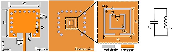
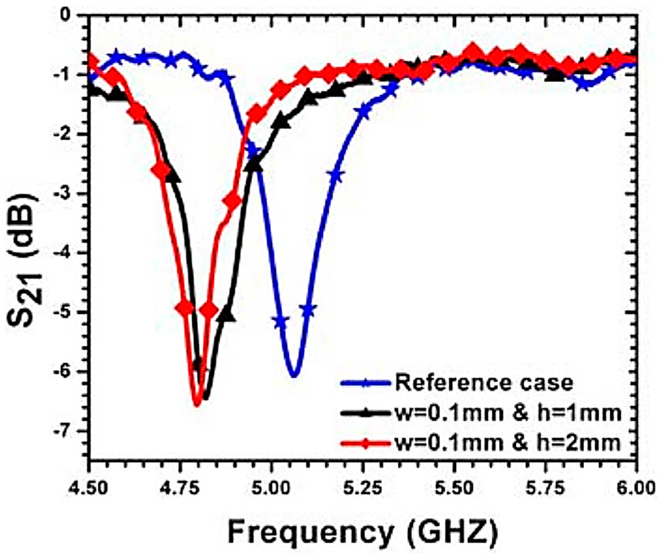
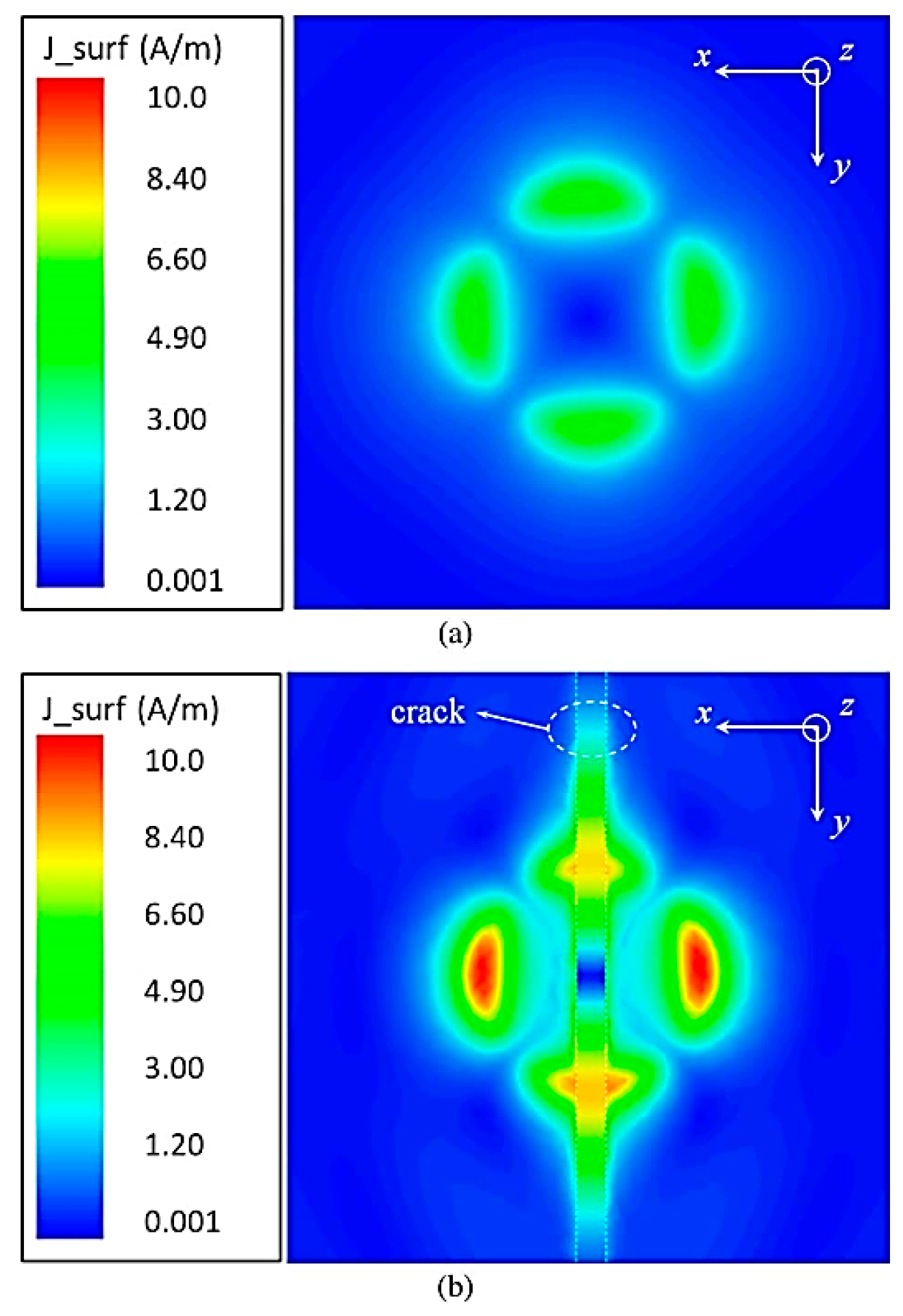
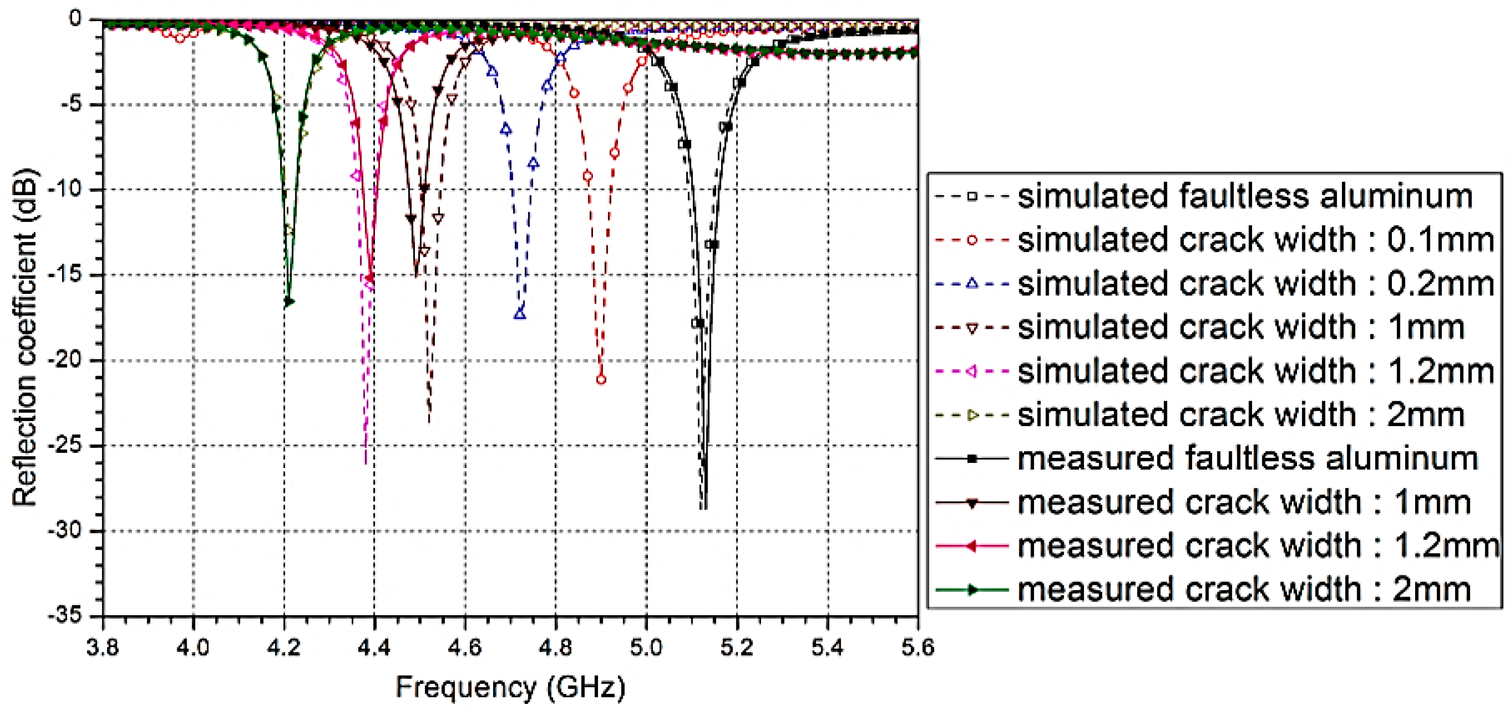
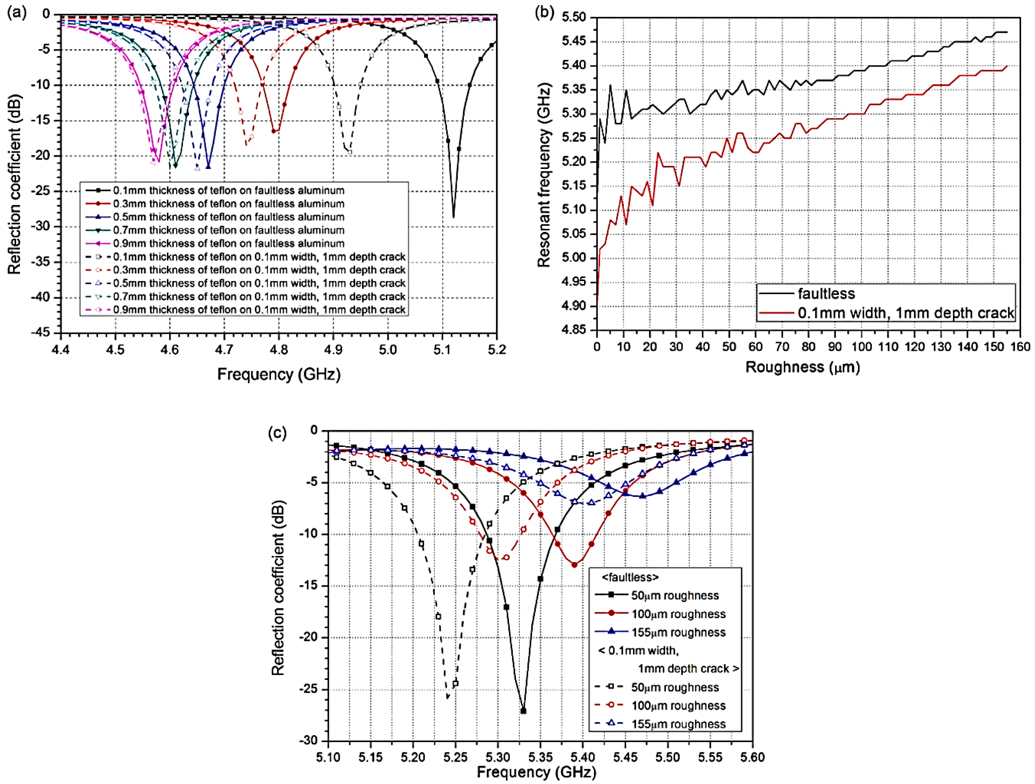
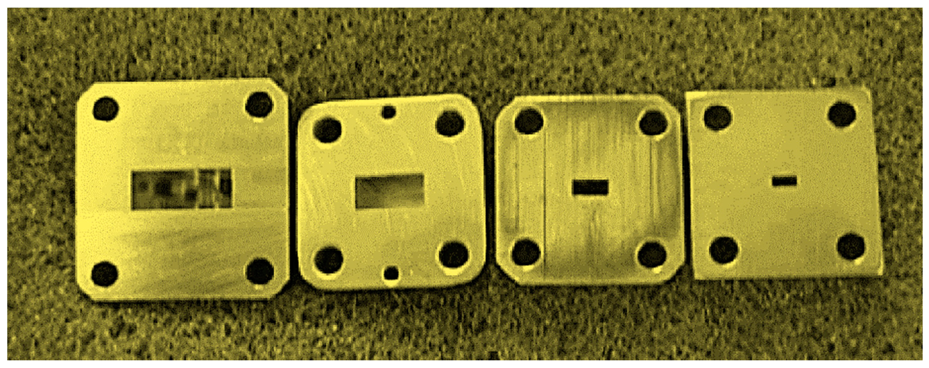
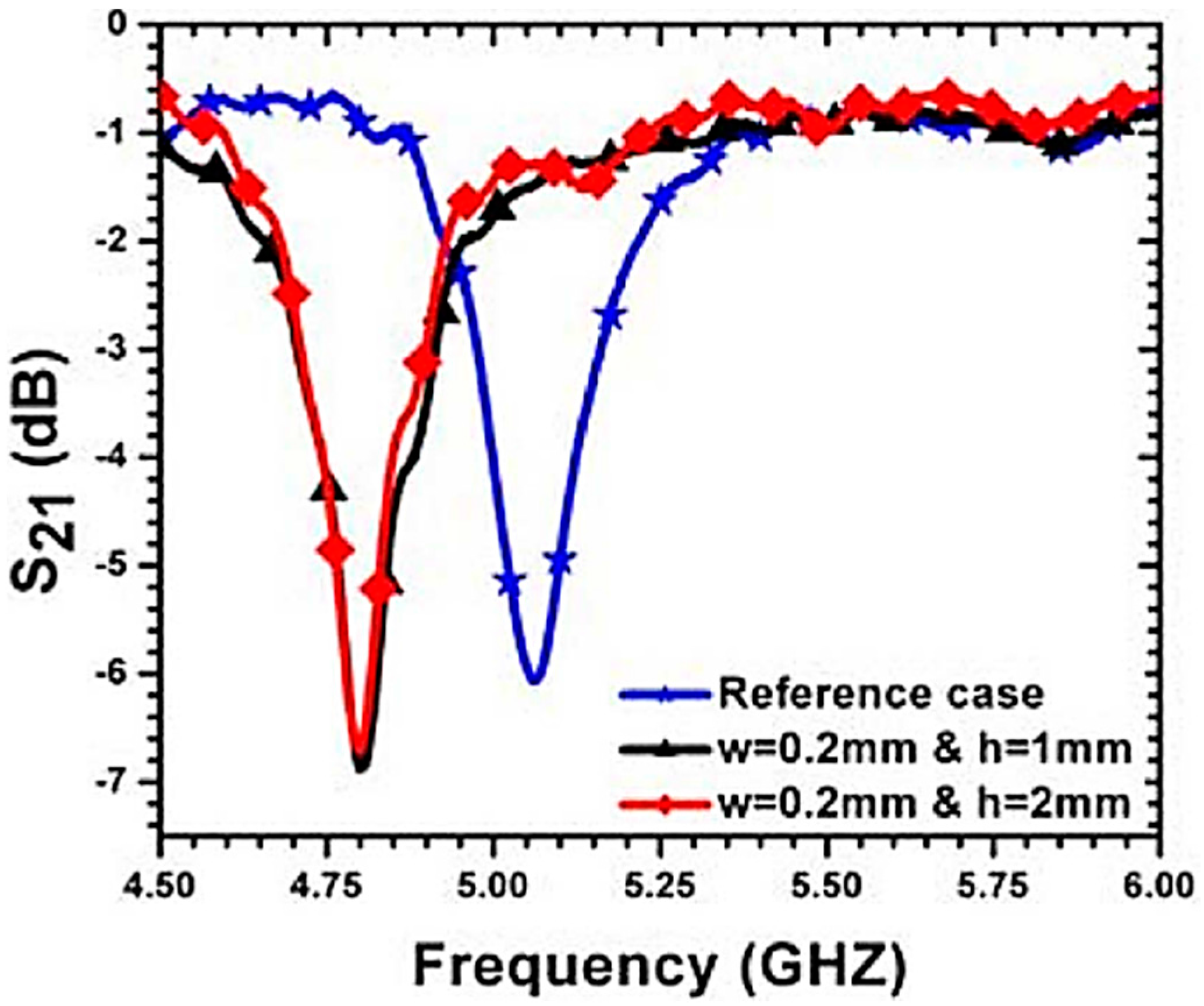
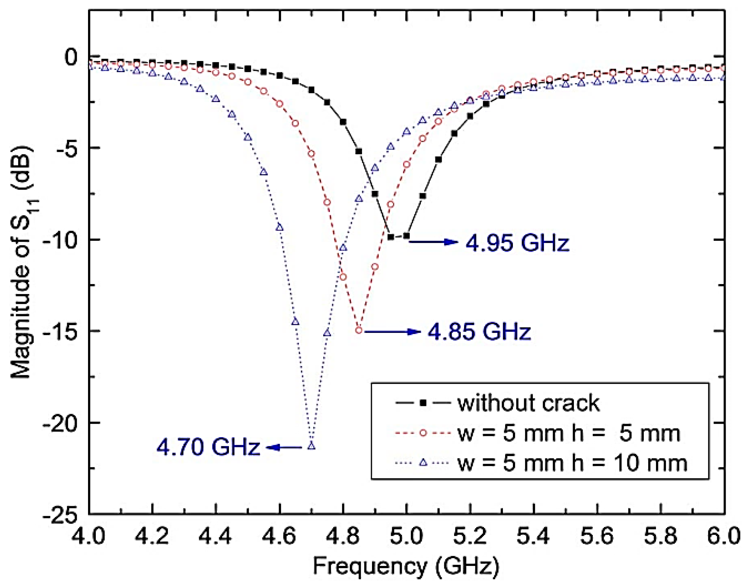
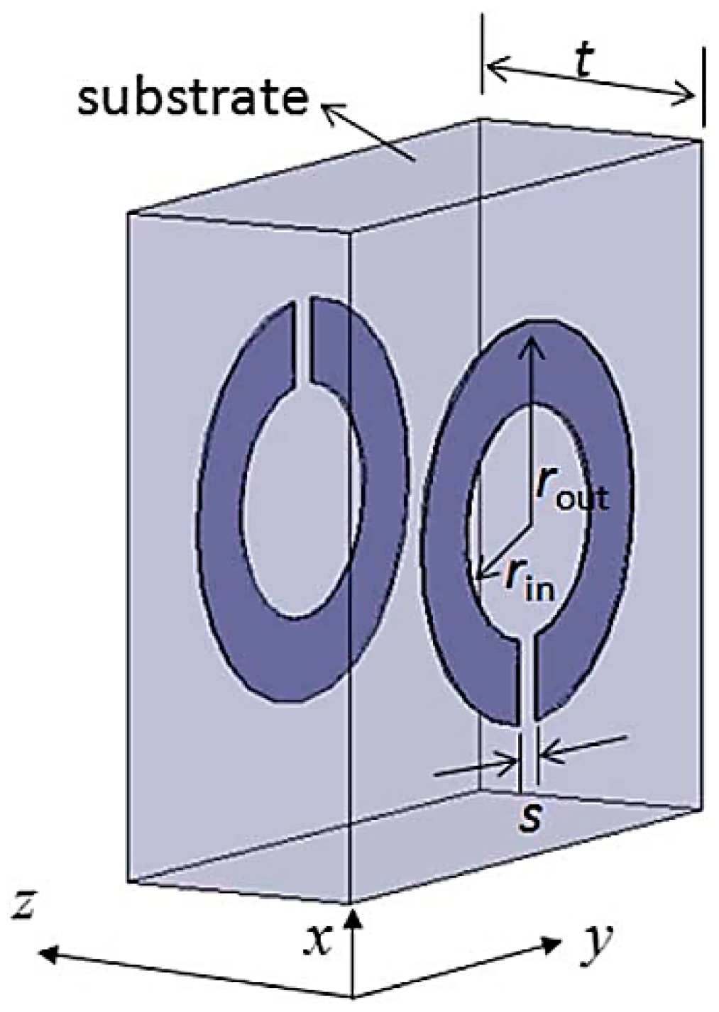
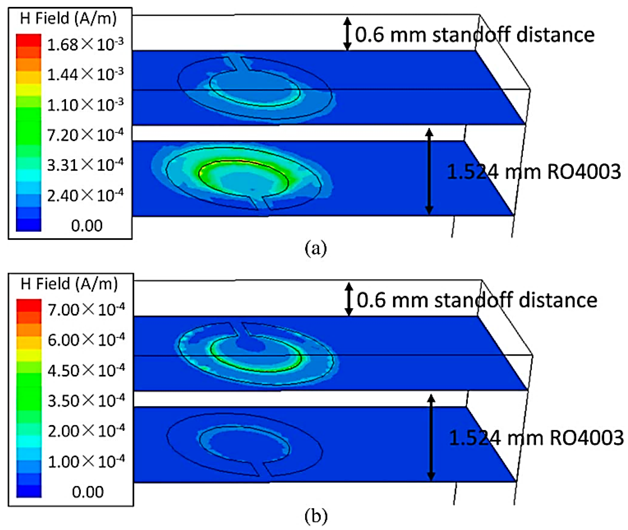
6. Complementary Split-Ring-Resonator-Loaded Substrate Integrated Waveguide Microwave Sensor for Crack Detection in Metallic Materials

In this section, a high Q and reduced CSRR-loaded SIW RF sensor for the detection of cracks in metals is described. An SIW technology combined with a CSRR with a high Q value are used for realizing high sensitivity. Furthermore, by loading the CSRR on the SIW cavity, the sensor is reduced in size with increased electrical size and can function below the cut-off frequency of the SIW. The presented sensor has a frequency change of 220 MHz for a 100-μm crack and 600 MHz for a 1-mm crack [41]. Additionally, the sensor operates at a low frequency (approximately 5 GHz) with improved resolution and sensitivity [42,43,44].
To replace the conventional waveguide, which is expensive and difficult to fabricate, here, the authors used an SIW cavity resonator with a high QF. The SIW initially reported in [45] not only has the benefit of low cost, but also is appropriate to co-exist with planar structures while preserving the advantages of the original waveguide cavity (high power capacity and high QF). The SIW consists of two parallel rows of metal vias implanted in the substrate, as shown in Figure 27. When the SIW is united with a CSRR, the CSRR mode and SIW mode are produced. The CSRR mode’s attained QF is greater than that of the SIW without the CSRR. Using this phenomenon of the CSRR mode, the sensitivity and resolution of the sensor can be enhanced. The authors have designed the CSRR to operate at approximately 5 GHz. This frequency avoids the use of an extensive measurement apparatus.
The simulated reflection coefficients of the SIW cavity with and without a CSRR are plotted in Figure 28. The width and length of the SIW cavity that yield a dominant resonant frequency of 7.29 GHz are chosen. Figure 29 shows the experimental setting used to sense the crack in the aluminum sheet. The presented RF sensor is placed on the aluminum sheet. The CSRR is patterned on the ground plane of the SIW. As discussed above, the surfaces of the metallic structures are covered with layers. Thus, a thin Teflon film with a thickness of 0.1 mm is used to model coating or paint on an aluminum plate with a 5-mm thickness, as shown in Figure 29. For crack modeling, cracks with 1-, 1.2- and 2-mm widths and 1- and 2-mm depths are created on a faultless metal plate. The frequency responses from the cracks with a 0.1-mm width and 0.2-mm width are observed only in the HFSS simulations because of the difficulty of creating cracks of 0.1 mm in width and 0.2 mm in width in practice. A photograph of the fabricated prototype of the sensor is shown in Figure 30. For the detection of a crack in metals, the sensor is scanned along the surface of the metals. To determine the availability of cracks, a faultless aluminum sample is used as a reference, as shown in Figure 30. The difference in the resonant frequency caused by the crack is recorded using an HP 8510C VNA.
Figure 31 shows the variations in the reflection coefficients when the sensor is located on cracks with several widths; the depth of the crack is maintained at 1 mm. The changes in the resonant frequency due to crack widths of 0.1 mm and 2 mm are 220 MHz and 980 MHz, respectively. When the crack width increases, the resonant frequency tends to decrease. As shown in Figure 32, differences in the reflection coefficients are observed when the sensor is positioned above the cracks of various widths (the depth of the crack is maintained at 2 mm). The changes in the resonant frequency due to the crack widths of 0.1 mm and 2 mm are 280 MHz and 1080 MHz, respectively. The resonant frequency tends to decrease as the crack width increases. To confirm the effect of Teflon thickness, the simulated reflection coefficients are plotted at different thickness of Teflon (t = 0.1, 0.3, 0.5, 0.7 and 0.9 mm) in Figure 33. The resonant frequencies of the faultless aluminum decrease as the thickness of the Teflon coating increases. That is, the resonant frequencies are 5.12, 4.79, 4.67, 4.61 and 4.58 GHz at t = 0.1, 0.3, 0.5, 0.7 and 0.9 mm, respectively. In addition, these frequencies are equated with the resonant frequencies of the faulty aluminum (for a 0.1-mm-width and 1-mm-depth crack). Frequency differences between the faultless and faulty aluminum sheets are 220, 50, 20, 10 and 10 MHz at t = 0.1, 0.3, 0.5, 0.7 and 0.9 mm, respectively. No frequency change can be observed after 0.9 mm in thickness.
In this section, a high Q and compact CSRR-loaded SIW sensor was proposed for detecting cracks in metals. An SIW cavity and a CSRR were used in combination for the detection and sensing of cracks covered by dielectric coatings. The SIW crack sensor operated at approximately 5 GHz, with a shift of 630 MHz in the resonant frequency observed for a crack of 1 mm in width and 1 mm in depth. Additionally, the sensor reveals a wide variety of resonant-frequency changes with a high QF (i.e., greater than 148). These aspects increase the resolution and sensitivity of the proposed sensor. When compared to other RF crack detection sensors, the proposed sensor functions at a lower frequency and has higher resolution and sensitivity.

7. Conclusions

There are many traditional non-destructive detection and evaluation techniques; however, near-field millimeter waves and microwave methods have recently shown promise for augmenting currently available non-destructive techniques. We have reviewed developments made until now in this area; we showed several promising microwave scanning techniques and also several candidates for future applications; these non-contact methods have the ability to identify and evaluate cracks and describe their different physical properties. The methods discussed in this article focused on filters using DBRs, CSRRs for the perturbation of electric fields, waveguide probe-loaded CSRRs and SIW technology for the detection of sub-millimeter surface and subsurface cracks.

Acknowledgments

This work was supported by a National Research Foundation of Korea (NRF) grant funded by the Korean government (MSIP) (No. 2014R1A2A1A11050010).

Author Contributions

Muhammad Usman Memon (first author) contributed in gathering data from literature, organization, acquiring permissions and write up of the manuscript. Sungjoon Lim (second author) contributed with the revision and proof reading.

Conflicts of Interest

The authors declare no conflict of interest.

References

  1. Prosser, W. Acoustic Emission. In Nondestructive Evaluation; CRC Press: Cleveland, OH, USA, 2002. [Google Scholar]
  2. Shull, P. Eddy Current. In Nondestructive Evaluation; CRC Press: Cleveland, OH, USA, 2002. [Google Scholar]
  3. Shull, P.; Joseph, K.; Lindgren, A.; Hagemaier, D. Magnetic Particle. In Nondestructive Evaluation; CRC Press: Cleveland, OH, USA, 2002. [Google Scholar]
  4. Shull, P.; Tittmann, B. Ultrasound. In Nondestructive Evaluation; CRC Press: Cleveland, OH, USA, 2002. [Google Scholar]
  5. Hruby, R.J.; Feinstein, L. A Novel Nondestructive, Noncontacting Method of Measuring the Depth of Thin Slits and Cracks in Metals. Rev. Sci. Instrum. 1970, 41, 679. [Google Scholar] [CrossRef]
  6. Husain, A.; Ash, E.A. Microwave Scanning Microscopy for Non-Destructive Testing. In Proceedings of the 5th European Microwave Conference, Hamburg, Germany, 1–4 September 1975; pp. 213–217.
  7. Bahr, A. Microwave Eddy-Current Techniques for Quantitative Nondestructive Evaluation. In Eddy-Current Characterization of Materials and Structures; ASTM International: West Conshohocken, PA, USA, 1981; pp. 311–331. [Google Scholar]
  8. Bahr, A.J. Microwave Nondestructive Testing Methods. In Nondestructive Testing Monographs and Tracts; Gordon and Breach Science Publishers: New York, NY, USA, 1982. [Google Scholar]
  9. Yeh, C. Detection and sizing of surface cracks in metals using open-ended rectangular waveguides. Master’s Thesis, Colorado State University, Fort Collins, CO, USA, July 1994. [Google Scholar]
  10. Yeh, C.Y.; Zoughi, R. A Novel Microwave Method for Detection of Long Surface Cracks in Metals. IEEE Trans. Instrum. Meas. 1994, 43, 719–725. [Google Scholar]
  11. Yeh, C.; Zoughi, R. Microwave detection of finite surface cracks in metals using rectangular waveguides. Res. Nondestruct. Eval. 1994, 6, 35–55. [Google Scholar] [CrossRef]
  12. Yeh, C.-Y.; Ranu, E.; Zoughi, R. A novel microwave method for surface crack detection using higher order waveguide modes. Mater. Eval. 1994, 52, 676–681. [Google Scholar]
  13. Huber, C. Electromagnetic modeling of exposed and covered surface crack detection using open-ended waveguides. Master’s Thesis, Colorado State University, Fort Collins, CO, USA, July 1996. [Google Scholar]
  14. Huber, C.; Abiri, H.; Ganchev, S.I.; Zoughi, R. Analysis of the “crack characteristic signal” using a generalized scattering matrix representation. IEEE Trans. Microw. Theory Tech. 1997, 45, 477–484. [Google Scholar] [CrossRef]
  15. Huber, C.; Abiri, H.; Ganchev, S.I.; Zoughi, R. Modeling of surface hairline-crack detection in metals under coatings using an open-ended rectangular waveguide. IEEE Trans. Microw. Theory Tech. 1997, 45, 2049–2057. [Google Scholar] [CrossRef]
  16. Qaddoumi, N.; Ranu, E.; McColskey, J.D.; Mirshahi, R.; Zoughi, R. Microwave Detection of Stress-Induced Fatigue Cracks in Steel and Potential for Crack Opening Determination. Res. Nondestruct. Eval. 2000, 12, 87–103. [Google Scholar] [CrossRef]
  17. Zoughi, R. Microwave Non-Destructive Testing and Evaluation Principles; Springer: Heidelberg, Germany, 2000. [Google Scholar]
  18. Park, H.H.; Cho, Y.H.; Eom, H.J. Surface crack detection using flanged parallel-plate waveguide. Electron. Lett. 2001, 37, 1526–1527. [Google Scholar] [CrossRef]
  19. Mazlumi, F.; Sadeghi, S.H.H.; Moini, R. Interaction of Rectangular Open-Ended Waveguides With Surface Tilted Long Cracks in Metals. IEEE Trans. Instrum. Meas. 2006, 55, 2191–2197. [Google Scholar] [CrossRef]
  20. Campbell, H.; Bastidas, F.R.; Hughes, D.; Zoughi, R. Laboratory statistical analysis of new microwave dominant mode and higher-order mode probe designs. Master’s Thesis, Colorado State University, Fort Collins, CO, USA, July 2000. [Google Scholar]
  21. Campbell, H. Optimal open-ended waveguide probe design for surface crack detection in metals at microwave frequencies. Master’s Thesis, Colorado State University, Fort Collins, CO, USA, July 2001. [Google Scholar]
  22. Wang, Y. Modeling of surface crack detection using open-ended coaxial probes. Master’s Thesis, Colorado State University, Fort Collins, CO, USA, July 1999. [Google Scholar]
  23. Wang, Y.; Zoughi, R. Interaction of surface cracks in metals with open-ended coaxial probes at microwave frequencies. Mater. Eval. 2000, 58, 1228–1234. [Google Scholar]
  24. Wang, N. Open-ended coaxial probes for covered surface crack detection and evaluation in metals at microwave frequencies. Master’s Thesis, Colorado State University, Fort Collins, CO, USA, July 2001. [Google Scholar]
  25. Wang, N.; Zoughi, R. Moment method solution for modeling the interaction of open ended coaxial probes and surface cracks in metals. Mater. Eval. 2002, 60, 1253–1258. [Google Scholar]
  26. Ghasr, M.T.; Ying, K.P.; Zoughi, R. SAR imaging for inspection of metallic surfaces at millimeter wave frequencies. In Proceedings of the 2014 IEEE International Instrumentation and Measurement Technology Conference (I2MTC), Montevideo, Uruguay, 12–15 May 2014; pp. 1202–1206.
  27. Pozar, D. Microwave Engineering, 4th ed.; Addison Wesley: New York, NY, USA, 1990. [Google Scholar]
  28. Zoughi, R.; Kharkovsky, S. Microwave and millimetre wave sensors for crack detection. Fatigue Fract. Eng. Mater. Struct. 2008, 31, 695–713. [Google Scholar] [CrossRef]
  29. Kerouedan, J.; Qu, P.; Talbot, P.; de Blasi, S.; le Brun, A. Detection of micro-cracks on metal surfaces using near-field microwave dual-behavior resonator filters. Meas. Sci. Technol. 2008, 19, 10. [Google Scholar] [CrossRef]
  30. Tabib-Azar, M.; Shoemaker, N.S.; Harris, S. Non-destructive characterization of materials by evanescent microwaves. Meas. Sci. Technol. 1993, 4, 583–590. [Google Scholar] [CrossRef]
  31. Wang, R.; Li, F.; Tabib-Azar, M. Calibration methods of a 2 GHz evanescent microwave magnetic probe for noncontact and nondestructive metal characterization for corrosion, defects, conductivity, and thickness nonuniformities. Rev. Sci. Instrum. 2005, 76, 054701. [Google Scholar] [CrossRef]
  32. Quendo, C.; Rius, E.; Person, C. Narrow bandpass filters using dual-behavior resonators. IEEE Trans. Microw. Theory Tech. 2003, 51, 734–743. [Google Scholar] [CrossRef]
  33. Quendo, C.; Rius, E.; Person, C. Narrow bandpass filters using dual-behavior resonators based on stepped-impedance stubs and different-length stubs. IEEE Trans. Microw. Theory Tech. 2004, 52, 1034–1044. [Google Scholar] [CrossRef]
  34. Wei, T.; Xiang, X.-D.; Wallace-Freedman, W.G.; Schultz, P.G. Scanning tip microwave near-field microscope. Appl. Phys. Lett. 1996, 68, 3506. [Google Scholar] [CrossRef]
  35. Imtiaz, A.; Anlage, S.M. Effect of tip geometry on contrast and spatial resolution of the near-field microwave microscope. J. Appl. Phys. 2006, 100, 044304. [Google Scholar] [CrossRef]
  36. Talanov, V.V.; Scherz, A.; Schwartz, A.R. A Microfabricated Near-Field Scanned Microwave Probe for Noncontact Dielectric Constant Metrology of Low-k Films. In Proceedings of the 2006 IEEE MTT-S International Microwave Symposium Digest, San Francisco, CA, USA, 11–16 June 2006; pp. 1618–1621.
  37. Kleismit, R.A.; Kazimierczuk, M.K.; Kozlowski, G. Sensitivity and resolution of evanescent microwave microscope. IEEE Trans. Microw. Theory Tech. 2006, 54, 639–647. [Google Scholar] [CrossRef]
  38. Albishi, A.M.; Boybay, M.S.; Ramahi, O.M. Complementary Split-Ring Resonator for Crack Detection in Metallic Surfaces. IEEE Microw. Wirel. Compon. Lett. 2012, 22, 330–332. [Google Scholar] [CrossRef]
  39. Albishi, A.; Ramahi, O.M. Detection of surface and subsurface cracks in metallic and non-metallic materials using a complementary split-ring resonator. Sensors 2014, 14, 19354–19370. [Google Scholar] [CrossRef] [PubMed]
  40. Hu, B.; Ren, Z.; Boybay, M.S.; Ramahi, O.M. Waveguide probe loaded with split-ring resonators for crack detection in metallic surfaces. IEEE Trans. Microw. Theory Tech. 2014, 62, 871–878. [Google Scholar] [CrossRef]
  41. Yun, T.; Lim, S. Sensors and Actuators A: Physical High-Q and miniaturized complementary split ring resonator-loaded substrate integrated waveguide microwave sensor for crack detection in metallic materials. Sens. Actuators A. Phys. 2014, 214, 25–30. [Google Scholar] [CrossRef]
  42. Dong, Y.D.; Yang, T.; Itoh, T. Substrate integrated waveguide loaded by complementary split-ring resonators and its applications to miniaturized waveguide filters. IEEE Trans. Microw. Theory Tech. 2009, 57, 2211–2223. [Google Scholar] [CrossRef]
  43. Ge, Z.-C.; Zhang, W.-X.; Liu, Z.-G.; Gu, Y.-Y. Broadband and high-gain printed antennas constructed from Fabry-Perot resonator structure using EBG or FSS cover. Microw. Opt. Technol. Lett. 2006, 48, 1272–1274. [Google Scholar] [CrossRef]
  44. Zhang, Q.-L.; Yin, W.-Y.; He, S.; Wu, L.-S. Evanescent-Mode Substrate Integrated Waveguide (SIW) Filters Implemented with Complementary Split Ring Resonators. Prog. Electromagn. Res. 2011, 111, 419–432. [Google Scholar] [CrossRef]
  45. Deslandes, D.; Wu, K. Single-substrate integration technique of planar circuits and waveguide filters. IEEE Trans. Microw. Theory Tech. 2003, 51, 593–596. [Google Scholar] [CrossRef]
Figure 1. Front view of the flanges and apertures of standard rectangular waveguides for the (from left to right) K-, Ka-, V-, and W-bands (from [28]; copyright © 2008; reproduced with permission).
Metals 06 00172 g001
Figure 2. Microstrip resonator design: (a) complete structure; and (b) zoomed in on electric dipole (from [29]; copyright © 2008; redesigned with permission).
Metals 06 00172 g002
Figure 3. Photograph of the experimental setup (from [29]; copyright © 2008; reproduced with permission).
Metals 06 00172 g003
Figure 4. Schematic drawing of the electric dipole probe above a notch. W, h and L represent the width, depth and length of the notch, respectively. d is the probe-to-metal distance (from [29]; copyright © 2008; redesigned with permission).
Metals 06 00172 g004
Figure 5. Measured reflection parameter S11 versus frequency above faultless metal and above a 200-μm-wide notch for a probe-to-metal distance d = 50 μm (from [29]; copyright © 2008; redesigned with permission).
Metals 06 00172 g005
Figure 6. 1D scans (x direction) above a stainless steel plate with a 200-μm-wide notch measured with the electric dipole probe for probe-to-metal distances d of 50 and 75 μm, respectively. Variations of the resonance frequency (∆fr) as a function of the x-position; x = 0 corresponds to the middle of the notch (from [29]; copyright © 2008; redesigned with permission).
Metals 06 00172 g006
Figure 7. First-order dual-behavior resonator (DBR) band-pass filter (BPF): (a) design and (b) reflection (S11) and transmission (S21) parameters (from [29]; copyright © 2008; redesigned with permission).
Metals 06 00172 g007
Figure 8. Schematic of the first-order DBR probe (from [29]; copyright © 2008; redesigned with permission).
Metals 06 00172 g008
Figure 9. Photograph of the first-order DBR probe above the stainless steel plate (from [29]; copyright © 2008; adopted with permission).
Metals 06 00172 g009
Figure 10. Measured transmission parameter S21 of the 10-μm-wide HF stub filter set at d = 50 μm above a faultless metal plate and a 200-μm-wide surface notch (from [29]; copyright © 2008; redesigned with permission).
Metals 06 00172 g010
Figure 11. 1D scans (x-direction) above a stainless steel plate with a 200-μm-wide notch measured using the 50- and 100-μm-wide high-frequency stub filters for a probe-to-metal distance d = 50 μm. Variations of the high-frequency stub frequency (∆fHF) as a function of the x position; x = 0 corresponds to the middle of the notch (from [29]; copyright © 2008; redesigned with permission).
Metals 06 00172 g011
Figure 12. Complementary split-ring resonator (CSRR) printed on the ground plane of a microstrip line (from [38]; copyright © IEEE 2012; reproduced with permission).
Metals 06 00172 g012
Figure 13. Schematic showing the microstrip line fed CSRR sensor and the scanning procedure (from [38]; copyright © IEEE 2012; reproduced with permission).
Metals 06 00172 g013
Figure 14. Minimum transmission of the sensor for a crack width (w) of 100 μm as compared to solid aluminum. For Case 1, the crack depth (h) is 200 μm. For Case 2, the crack depth (h) is 100 μm (from [37]; copyright © IEEE 2012; reproduced with permission).
Metals 06 00172 g014
Figure 15. Minimum transmission of the sensor for a crack width (w) of 200 μm as compared to solid aluminum. For Case 1, the crack depth (h) is 200 μm. For Case 2, the crack depth (h) is 100 μm (from [38]; copyright © IEEE 2012; reproduced with permission).
Metals 06 00172 g015
Figure 16. Distribution of the surface current on the aluminum board with/without a long crack. The operation frequency is 4.70 GHz. The distance between the aluminum board and loop is 5 mm. The width and depth of the crack are 5 and 10 mm, respectively. (a) Magnitude of the surface current without a crack; (b) magnitude of surface current with a crack (from [40]; copyright © IEEE 2014; reused with permission).
Metals 06 00172 g016
Figure 17. Reflection coefficient of the loop above perfect and defective aluminum boards. w and h are the width and depth of the crack. w is equal to λ0/12, where λ0 is the free-space wavelength (i.e., 5 GHz).
Metals 06 00172 g017
Figure 18. Schematic showing a waveguide probe positioned above a metal board. d is the standoff distance between the waveguide load and the surface of the metal plate (from [40]; copyright © IEEE 2014; reproduced with permission).
Metals 06 00172 g018
Figure 19. Geometry and dimensions of the SRR resonators. The inner and outer radii of the circular strips are rin = 0.7 mm and rout = 1.2 mm, respectively. The gap width of the circular strip is s = 0.2 mm. The thickness of the substrate is t = 1.524 mm (from [40]; copyright © IEEE 2014; reproduced with permission).
Metals 06 00172 g019
Figure 20. Magnetic field distributions at the resonance frequencies of the SRR cells: (a) at 14.53 GHz and (b) at 16.24 GHz (from [40]; copyright © IEEE 2014; reproduced with permission).
Metals 06 00172 g020
Figure 21. Diagram of the method for detecting long cracks on a metal surface (from [40]; copyright © IEEE 2014; reproduced with permission).
Metals 06 00172 g021
Figure 22. Reflection coefficient of the probe with and without a crack. The width and depth of the crack are 0.3 and 2 mm, respectively. The standoff distance between the PCB and the aluminum surface is 0.6 mm in both cases (from [40]; copyright © IEEE 2014; reproduced with permission).
Metals 06 00172 g022
Figure 23. (a) Photograph of the real probe; (b) photographs of the top and bottom views of the PCB with the SRR array (from [40]; Copyright © IEEE 2014; reproduced with permission).
Metals 06 00172 g023
Figure 24. Configuration of the experimental setup. The probe is fixed to the support by a tight fit craft and can be moved along the y axis by turning the handle. The precision for moving the probe is 0.1 mm/step (from [40]; copyright © IEEE 2014; reproduced with permission).
Metals 06 00172 g024
Figure 25. Experimental results for the frequency response of the waveguide probe without the aluminum plate (from [40]; copyright © IEEE 2014; reproduced with permission).
Metals 06 00172 g025
Figure 26. Experimental results for testing cracks with different widths: (a) magnitude response for the probe position and (b) phase response for the probe position. “w” is the width of the crack (from [40]; copyright © IEEE 2014; reproduced with permission).
Metals 06 00172 g026
Figure 27. Planar view of the CSRR-loaded substrate-integrated-waveguide (SIW): (a) top view, (b) bottom view, (c) CSRR and (d) lossless equivalent circuit model of the CSRR (from [41]; copyright © 2014; reproduced with permission).
Metals 06 00172 g027
Figure 28. Simulated reflection coefficients of the SIW cavity (without a CSRR) and the CSRR-loaded SIW cavity (from [41]; copyright © 2014; reproduced with permission).
Metals 06 00172 g028
Figure 29. Measurement environment: (a) side view and (b) cross-sectional view (from [41]; copyright © 2014; reproduced with permission).
Metals 06 00172 g029
Figure 30. Fabricated sensor and aluminum sample: (a) top and bottom views of the sensor and (b) aluminum sample; (from [41]; copyright © 2014; reproduced with permission).
Metals 06 00172 g030
Figure 31. Simulated and measured results of the reflection coefficient for a crack depth of 1 mm (from [41]; copyright © 2014; reproduced with permission).
Metals 06 00172 g031
Figure 32. Simulated and measured results of the reflection coefficient for a crack depth of 2 mm (from [41]; copyright © 2014; reproduced with permission).
Metals 06 00172 g032
Figure 33. (a) Simulated reflection coefficients at different thicknesses of Teflon; (b) simulated resonant frequencies at different roughness levels on the top Teflon surface; and (c) the simulated reflection coefficients at 50 μm, 100 μm and 155 µm roughness levels on the top Teflon surface for faultless and cracked (0.1 mm in width and 1 mm in depth) aluminum (from [41]; copyright © 2014; adopted with permission).
Metals 06 00172 g033

