

Growth of a Sub-Centimeter-Sized CsPbBr3 Bulk Single Crystal Using an Anti-Solvent Precipitation Method

International School of Microelectronics, Dongguan University of Technology, Dongguan 523808, China
Symmetry 2024, 16(3), 332; https://doi.org/10.3390/sym16030332
Submission received: 29 December 2023
/
Revised: 26 February 2024
/
Accepted: 5 March 2024
/
Published: 9 March 2024
(This article belongs to the Special Issue Advances in Perovskites: Growth, Characterization and Optoelectronic Devices)
Abstract
:A facile and low-cost strategy to fabricate CsPbBr3 single crystals is essential for developing perovskite optoelectronic devices. Herein, we have presented a room temperature anti-solvent precipitate method for growing sub-centimeter-sized CsPbBr3 single crystals. The as-prepared CsPbBr3 single crystal has an orthorhombic structure, and phase transition occurs as the measured temperature increases. The as-grown CsPbBr3 single crystal also shows abundant surface morphologies including footsteps, precipitated crystals, cracks, and pits. Subsequently, a metal–semiconductor–metal (MSM)-structured photodetector was fabricated based on the CsPbBr3 single crystal. Under 525 nm green light illumination, the photodetector exhibits an obvious response and the photocurrent linearly increases with the increase in the light intensity. The rise time of the photodetector increases from 0.82 s to 2.19 s as the light intensity is enhanced from 15 mW/cm2 to 160 mW/cm2, indicating that more time is required to reach to a stable photocurrent. However, the decay time is as fast as ~0.82 ms, irrelevant of the light intensity. The photocurrent, under continuous light illumination, was further studied and this indicates that a stronger light intensity can accelerate the attenuation of the device.
1. Introduction
Recently, hybrid organic–inorganic perovskite has attracted great interest as a promising candidate for constructing optoelectronic devices including light emitting diodes (LEDs), solar cells, and photodetectors [1,2,3,4,5]. Among them, a photodetector is a device which can convert incident light into an electrical signal, with applications in optical communication and imaging. For instance, Chang et al. report a high-performance (FASnI3)0.1(MAPbI3)0.9-based self-powered near-infrared photodetector with a broad linear dynamic range of 163.5 dB, which is a potential candidate for low-cost near-infrared photodetection [6]. Nevertheless, owing to the instability in light, heat, and moisture conditions, the practical applications of hybrid perovskites are still to be determined [7,8]. All inorganic perovskites, such as bismuth halide perovskite (Cs3Bi2X9, (X = I, Br, Cl)) and Pb-based perovskite (CsPbX3, (X = I, Br, Cl)), have been well regarded because of their high environmental stability [9,10,11,12]. The all-inorganic CsPbX3 reveals a large absorption co-efficiency of ~2 × 105 cm−1 and a high carrier mobility of ~1000 cm2 V−1 S−1 [13,14]. As a member of the all-inorganic cesium lead halides family, CsPbBr3 has a direct bandgap of 2.2 eV~2.35 eV, which shows its great potential as a visible band photodetector. Currently, numerous studies regarding CsPbBr3-based photodetectors have been reported, while the stability of these devices under strong light illumination is still rarely considered.
Up to now, different kinds of CsPbBr3, including low-dimensional structures (nano crystals, nanowires, nano rings) [15,16,17] and large-sized bulk single crystals [18,19,20], have been fabricated. Though these low-dimensional structures present interesting and novel physical characteristics owing to their size confinement effects, the bulk single crystal group may show many more advantages in their practical applications. Two methods, including the Bridgman method [18,19,20] and the anti-solvent precipitated method [21,22], are normally employed to fabricate large-scale CsPbBr3 single crystals. The former one normally grows crystals at high temperature (>500 °C) and under vacuum conditions, which requires an expensive growth facility. For example, He et al. [18] used a two-zone vertical furnace for CsPbBr3 single crystal growth; the growth temperature was as high as 590 °C and the initial pressure was less than 10−4 Torr. As a contrast, the anti-solvent precipitate method usually grows crystals at a low temperature and has a low cost. With the assistance of a good solvent and poor solvent, the CsPbBr3 in the solution is supersaturated and crystals are precipitated [23]. Rakita et al. prepared millimeter-sized CsPbBr3 crystals at 50~80 °C; the size and shape of the samples can be modulated through controlling the anti-solvent (acetonitrile or methanol) and UV illumination [24]. Ding et al. used methyl alcohol and ethanol as anti-solvents; orthogonal phase CsPbBr3 crystals with a (101) facet were grown in a saturated DMSO solution at 40 °C [25]. Therefore, the anti-solvent vapor-assisted crystallization method provides an economic and facile strategy for fabricating CsPbBr3 single crystals. Furthermore, it would be highly useful if the growth temperature could be lowered to room temperature. In this case, no heating facilities would be required and the growth processes would be simpler. Zhang et al. have successfully obtained CsPbBr3 single crystals with a length up to 42 mm using an improved anti-solvent method at room temperature [26], while their longest growth time lasted for 14 days. Furthermore, though the all-inorganic CsPbBr3 is much more stable than the organic–inorganic hybrid one, it is less stable than inorganic semiconductors like diamond [27] and ZnO [28]. In addition, the stability of CsPbBr3 photodetectors under continuous illumination with different light intensities is rarely considered.
Herein, we have fabricated sub-centimeter-sized CsPbBr3 bulk single crystals through a simple anti-solvent precipitate method. The growth temperature is room temperature, and only two glass beakers and one glass plate are needed during the growth processes. A temperature-dependent XRD measurement reveals the phase transitions of the CsPbBr3 single crystal at different temperatures. Surface morphology studies show abundant surface defects, indicating a different growth mechanism at room temperature. An MSM-structured photodetector is prepared based on the as-grown CsPbBr3 single crystal, in which Ohmic contact is realized by using a low-work-function InGa alloy as electrodes. The light-intensity-dependent photoresponse is studied and the rise time of the photodetector increases as the light intensity increases. Furthermore, the photocurrent continuously attenuates as the light intensity increases, which indicates the deterioration of the CsPbBr3 single crystal with the assistance of light illumination in an air atmosphere.
2. Materials and Methods
2.1. Materials
The reagents in this work were purchased from commercial corporations without any purification. Cesium bromide (CsBr, 99.9%) and lead bromide (PbBr2, 99.9%) were purchased from Alfa Aesar (China) Co., Ltd, Shanghai, China. Dimethyl sulfoxide (DMSO), methanol, and ethanol solvents were purchased from Sinopharm Chemical Reagent Co., Ltd, Beijing, China.
2.2. Growth of CsPbBr3 Single Crystal
The CsPbBr3 single crystals were synthesized using an anti-solvent precipitation method; the growth processes are schematically shown in Figure 1. Firstly, a CsBr:PbBr2 mixture, with mole ratio of 1:1, was completely dissolved into 8 mL of DMSO solvent via continuous stirring for 1 h (Figure 1a,b). Then, the saturated solution was loaded into a beaker (Figure 1b,c) loaded with methanol solvent, and the beaker was sealed with a glass mat. As such, the methanol gradually evaporated into the saturated solution, and thus the CsPbBr3 single crystals precipitated onto the bottom of the container. The single crystals were synthesized at room temperature for 72 h. After that, the CsPbBr3 single crystals were washed with anhydrous ethanol and then dried by nitrogen gun. The processing (washing and drying) time was 1 h. The total growth procedure took 74 h.
2.3. Characterization
The crystal structure of the CsPbBr3 single crystal was estimated through a temperature-dependent X-ray diffraction (XRD) measurement with a Cu K-line (1.54 Å) as the light source. The optical characteristics of the CsPbBr3 single crystal were studied using four characterization methods including photoluminescence (PL), a PL decay trace, transmittance, and absorption spectra. The phonon vibration property of the CsPbBr3 single crystal was measured by its room temperature Raman spectra, with 532 nm and 785 nm lasers as excitation. Elemental analysis was employed using an energy-dispersive spectrometer (EDS). The surface morphology of the CsPbBr3 single crystal was observed by scanning electron microscope (SEM).
2.4. Device Fabrication and Measurement
A pair of symmetric InGa electrodes were bladed and coated onto the CsPbBr3 single crystal. The photoresponse of the photodetector was evaluated using a green-light LED (525 nm) as a light source and an electrochemical workstation as the electric signal collector. The light intensity of the LED can be modulated by adjusting the driven current. The stability of the photocurrent was also studied through a long-term current–time (I-T) measurement under the conditions of room temperature (~25 °C) and a relative humidity of 65%.
3. Results and Discussion
The crystal structure of the as-grown CsPbBr3 single crystal was studied by XRD measurements at different temperatures. As presented in Figure 2a, the room temperature XRD patterns reveal four diffraction peaks located at 15.07°, 15.23°, 30.36°, and 30.68°, which can be indexed as the XRD signals from the (002), (110), (004), and (220) facets [29,30]. A picture of the CsPbBr3 single crystals is presented in Figure S1 (Supplementary Materials); the length of the as-grown crystal ranges from ~0.2 cm to ~0.55 cm. Obviously, the shapes of the as-grown single crystals are not very regular. Thus, during the XRD measurement, both the (002) and (110) facets were exposed to the X-ray. According to previous reports, the crystal structure of CsPbBr3 growth at room temperature has been determined to be an orthorhombic structure [29,30]. The temperature-dependent XRD measurements were also performed in order to study the phase evolution of the CsPbBr3 single crystal. As presented in Figure 2b, considerable variations can be clearly observed as the tested temperature increases. As the tested temperature increases to 50 °C, the (004) and (220) XRD peaks slightly shift to a smaller angle, indicating the expansion of the lattice constant. In addition, the XRD intensity also decreases and the peak shape broadens. As the tested temperature increases to 100 °C, only one XRD peak can be observed, which is ascribed to the phase transition from orthorhombic to tetragonal. The XRD peaks tested at 200 °C and 300 °C are rather weak, and the CsPbBr3 further undergoes a phase transition from tetragonal to cubic. As the tested temperature increases to 400 °C, no XRD signals can be detected, indicating the amorphous nature of the material. The temperature-dependent phase evolution of CsPbBr3 is very interesting and is also verified by differential scanning calorimetry (DSC) measurements [31,32,33].
The PL spectrum of the CsPbBr3 single crystal is shown in Figure 3a, in which the wavelength of the excited light is 360 nm (one-photon excitation). A strong emission centered at 527 nm was detected, which is consistent with the bandgap of the CsPbBr3 single crystal [34,35] and a little longer than that of CsPbBr3 nanowires (519 nm) [36] and nanocrystals (511 nm) [37]. The time-resolved PL decay trace of the CsPbBr3 single crystal is presented in Figure 3b; its PL lifetime is determined to be as short as 1.86 ns, indicating the fast surface recombination of the photogenerated carrier, assisted by its trap state [32]. This PL lifetime is shorter than other reported values of CsPbBr3 single crystals [24,25,34,35]. The transmittance spectrum of the CsPbBr3 single crystal is revealed in Figure 3c, and it exhibits a transmittance of over 90% within the wavelengths longer than 560 nm. The crystal’s absorption spectrum is provided in Figure 3d; a clear absorption edge located at ~545 nm is determined, verifying the bandgap of 2.27 eV. Its Raman spectra is also measured in order to study the phonon vibration of the lattice. As shown in Figure 3e, five Raman peaks (A: 41.8 cm−1, B: 66.3 cm−1, C: 123.2 cm−1, D: 144.5 cm−1, E: 310 cm−1) can be observed under 785 nm laser excitation and the back scattering measurement configuration. This result agrees well with previous reports on CsPbBr3 quantum dots [38] and microspheres [30], which can be indexed as the eigenmodes of orthorhombic phase CsPbBr3. Its Raman spectrum under 532 nm green light excitation was also measured and is presented in the inset of Figure 3e. Apparently, a strong and broad emission was detected, which can be ascribed to the PL background of the CsPbBr3 single crystal. This is due to the bandgap of CsPbBr3 being close to the excitation wavelength. The EDS spectrum of the CsPbBr3 single crystal is presented in Figure 3f; the signals from the Cs, Pb, and Br can be clearly detected, and their atomic ratio is determined to be 1:1:3. Here, the C signal is inevitable during the EDS measurement and the Cu signal comes from the sample holder.
Detailed surface structures from different regions are observed by SEM, which is presented in Figure 4. Figure 4a presents a two-dimensional (2D) footstep morphology, which is controlled by a 2D nucleation mechanism and the motion of the derivative steps. From a previous report, we know that the step is along the (101) facet of the CsPbBr3 single crystal [25]. Several precipitated CsPbBr3 crystals with sizes ranging from tens of to two hundred nanometers can be found in Figure 4b. In addition, a large-sized (~3 μm) and disk-shape implanted CsPbBr3 crystal can also be observed, which is quite interesting and provides abundant morphology details of the surface. Figure 4c presents the surface morphology of another region; it has a riverbed-like morphology flushed by water. Undulating ravines and local cracking are clearly observed. Finally, rectangular and circle-shaped pits are detected in some regions and exhibited in Figure 4d. The abundant morphology of the as-prepared CsPbBr3 crystal grown at room temperature indicates localized insufficient reactants and an anisotropic growth rate. The surface defects will cause trap centers, which not only promote the decay of the PL lifetime, but also lead to a slow response of the CsPbBr3 photodetector (which will be discussed later). A specific area with irregular pits is selected to perform the EDS mapping measurement on; the elemental distributions on the regular surface and at the edges of the pits can be probed and compared. As presented in Figure 5, the disperse signals of the Cs, Pb, and Br elements are precisely mapped. Uniform distributions of the Cs, Pb, and Br elements are verified on the surface and the pit edges, while the EDS signals from the pit are much weaker than those from the surface, which could be due to the probed depth of the EDS detector.
The I-V curve of the CsPbBr3 MSM photodetector under dark is revealed in Figure 6a, which shows its linear characteristic. This could be owing to the Ohmic contact property between the InGa electrode and CsPbBr3; the dark current at the 5 V bias voltage is ~7 nA. As the photodetector is illuminated by the 525 nm green light (as shown in Figure 6b) the photocurrent boosts significantly, and the light to dark ratio is also enhanced as the light intensity increases from 15 mW/cm2 to 160 mW/cm2. Figure 6c summarizes the photocurrent of the photodetector, driven by a specific voltage, as a function of the light intensity. Apparently, the photocurrent linearly increases with the increase in the light intensity. This indicates that the photocurrent of the device is still beyond its saturated value even under a light intensity of 160 mW/cm2. The I-T curves of the CsPbBr3 MSM photodetector under an on–off switched illumination of 525 nm LED light with different light intensities is shown in Figure 6d, from which we can observe the repeatable and stable photoresponse behavior of the device. When the illumination is in its on state, the photocurrent sharply increases and then slowly reaches its saturated value under persistent light excitation. Once the illumination is in its off state, the photocurrent sharply decays to its initial value. Single-cycled I-T curves excited by different light intensities are extracted from Figure 6d and presented in Figure 6e. The rise time and decay time of the CsPbBr3 MSM photodetector under different light intensities are determined and summarized in Figure 6f. The decay times (from 90% to 10% of the maximum current) under different light intensities are all steadied at ~82 ms, indicating the fast recovery of the device. However, the rise time of the photodetector increases from 0.82 s to 2.19 s as the light intensity increases, meaning that a longer time is required to reach a saturated photocurrent as the light intensity increases.
As mentioned above, the all-inorganic perovskite CsPbBr3 is much more stable than its organic–inorganic counterparts like MAPbI3 or FAPbBr3. However, compared with all-inorganic semiconductors like GaN, SnO2, or ZnO, the stability of CsPbBr3 should be further improved [39,40]. Figure 7 shows the stability of the CsPbBr3 MSM photodetector under continuous illumination from a 525 nm green light with different light intensities. The tested temperature is ~25 °C (room temperature) and the relative humidity is 65%. Obviously, a stronger light intensity can accelerate the attenuation of the photocurrent. Under the light intensity of 160 mW/cm2, the times for the initial photocurrent to reach 95% and 90% of its initial value are 610 s and 1175 s. However, a weaker light intensity (36 mW/cm2 and 98 mW/cm2) contributes to a slower attenuation of the photocurrent. Under the light intensities of 98 mW/cm2 and 36 mW/cm2, the times for the initial photocurrent to reach 95% of its initial value are 2000 s and over 2300 s. Under light illumination, degradation of the photoresponse performance is inevitable. So, encapsulation in a waterproof layer is normally employed as an effective strategy for improving the stability of the CsPbBr3 device [41,42,43].
4. Conclusions
In conclusion, a facile anti-solvent solution method is introduced to grow sub-centimeter-sized CsPbBr3 bulk single crystals at room temperature. The crystal phase of the CsPbBr3 single crystal is systematically studied at different temperatures, which indicates a phase transition of orthorhombic → tetragonal → cubic → amorphous. The SEM images reveal that the as-grown CsPbBr3 single crystal has abundant surface morphologies including footsteps, precipitated crystals, cracks, and pits. Subsequently, an MSM-structured CsPbBr3 single crystal photodetector is fabricated using InGa as a pair of Ohmic electrodes. The photodetector shows a distinct response to 525 nm green light, and its photocurrent is linearly related to the light intensity. The decay time of the photodetector is as fast as 82 ms and independent of the light intensity, while the rise time of the photodetector is related to the light intensity and reaches 0.82 s to 2.19 s. The stability of the device is further studied and shows a significant attenuation of the photocurrent under stronger light illumination.
Supplementary Materials
The following supporting information can be downloaded at https://www.mdpi.com/article/10.3390/sym16030332/s1, Figure S1: a picture of the as-grown CsPbBr3 single crystals.
Funding
This work was financially supported by the National Natural Science Foundation of China (No. 52172149, 61705043) and a start-up fund from Dongguan University of Technology (221110144), as well as the Guangdong Provincial Key Laboratory Project (High-Performance Integrated Circuits and Systems Laboratory, No. 2023KSYS003).
Data Availability Statement
Data are contained within the article and Supplementary Materials.
Acknowledgments
The authors thank F. Yi for her helpful improvement of this manuscript. Parts of the crystals’ characterization were performed in Dongguan University of Technology’s Analytical and Testing Center.
Conflicts of Interest
The authors declare no conflicts of interest.
References
- Wang, W.J.; Cai, M.L.; Wu, Y.Z.; Ji, K.Y.; Cheng, B.; Liu, X.P.; Lv, H.; Dai, S.Y. Defect healing of MAPbI3 perovskite single crystal surface by benzylamine. Symmetry 2022, 14, 1099. [Google Scholar] [CrossRef]
- Li, W.; Wang, Z.M.; Deschler, F.; Gao, S.; Friend, R.H.; Cheetham, A.K. Chemically diverse and multifunctional hybrid organic-inorganic perovskites. Nat. Rev. Mater. 2017, 2, 16099. [Google Scholar] [CrossRef]
- Leguy, A.M.; Frost, J.M.; McMahon, A.P.; Sakai, V.G.; Kockelmann, W.; Law, C.; Li, X.E.; Foglia, F.; Walsh, A.; Regan, B.C.; et al. The dynamics of methylammonium ions in hybrid organic-inorganic perovskite solar cells. Nat. Commun. 2015, 6, 7124. [Google Scholar] [CrossRef] [PubMed]
- Do, H.H.; Kim, S.Y. Metal-organic frameworks based multifunctional materials for solar cells: A review. Symmetry 2023, 15, 1830. [Google Scholar] [CrossRef]
- Tian, W.; Zhou, H.P.; Li, L. Hybrid organic-inorganic perovskite photodetectors. Small 2017, 13, 1702107. [Google Scholar] [CrossRef] [PubMed]
- Chang, Z.Z.; Lu, Z.J.; Deng, W.; Shi, Y.D.; Sun, Y.Y.; Zhang, X.J.; Jie, J.S. Narrow-bandgap Sn-Pb mixed perovskite single crystals for high-performance near-infrared photodetectors. Nanoscale 2023, 15, 5053–5062. [Google Scholar] [CrossRef]
- Smith, I.C.; Hoke, E.T.; Solis-Ibarra, D.; McGehee, M.D.; Karunadasa, H.I. A layered hybrid perovskite solar-cell absorber with enhanced moisture stability. Angew. Chem. Int. Ed. 2014, 53, 11232–11235. [Google Scholar] [CrossRef]
- Li, Y.; Ji, L.; Liu, R.; Zhang, C.; Mak, C.H.; Zou, X.; Shen, H.-H.; Leu, S.-Y.; Hsu, H.Y. A review on morphology engineering for highly efficient and stable hybrid perovskite solar cells. J. Mater. Chem. A 2018, 6, 12842–12875. [Google Scholar] [CrossRef]
- Valastro, S.; Gavranovic, S.; Deretzis, I.; Vala, M.; Smecca, E.; Magna, A.L.; Alberti, A.; Castkova, K.; Mannino, G. Temperature-dependent excitonic band gap in lead-free bismuth halide low-dimensional perovskite single crystals. Adv. Opt. Mater. 2023, 2302397. [Google Scholar] [CrossRef]
- Hanqi, B.H.; Jiang, M.M.; Lin, C.X.; Liu, M.S.; Shi, D.N.; Kan, C.X. Flexible CsPbBr3 microwire photodetector with a performance enhanced by covering it with an Ag nanolayer. Cryst. Eng. Commun. 2022, 24, 7620–7631. [Google Scholar] [CrossRef]
- Su, L.X. Room temperature amplified spontaneous emissions in a sub-centimeter sized CsPbBr3 bulk single crystal. Opt. Express 2023, 31, 39020–39029. [Google Scholar] [CrossRef]
- Su, L.X. Room temperature growth of CsPbBr3 single crystal for asymmetric MSM structure photodetector. J. Mater. Sci. Technol. 2024, 187, 113–122. [Google Scholar] [CrossRef]
- Roo, J.D.; Ibáñez, M.; Geiregat, P.; Nedelcu, G.; Walravens, W.; Maes, J.; Martins, J.C.; Driessche, I.V.; Kovalenko, M.V.; Hens, Z. Highly dynamic ligand binding and light absorption coefficient of cesium lead bromide perovskite nanocrystals. ACS Nano 2016, 10, 2071–2081. [Google Scholar] [CrossRef] [PubMed]
- Yettapu, G.R.; Talukdar, D.; Sarkar, S.; Swarnkar, A.; Nag, A.; Ghosh, P.; Mandal, P. Terahertz conductivity within colloidal CsPbBr3 perovskite nanocrystals: Remarkably high carrier mobilities and large diffusion lengths. Nano Lett. 2016, 16, 4838–4848. [Google Scholar] [CrossRef] [PubMed]
- Dutta, A.; Dutta, S.K.; Adhikari, S.; Pradhan, N. Tuning the size of CsPbBr3 nanocrystals: All at one constant temperature. ACS Energy Lett. 2018, 3, 329–334. [Google Scholar] [CrossRef]
- Shang, Q.; Li, C.; Zhang, S.; Liang, Y.; Liu, Z.; Liu, X.; Zhang, Q. Enhanced optical absorption and slowed light of reduced-dimensional CsPbBr3 nanowire crystal by exciton-polariton. Nano Lett. 2020, 20, 1023–1032. [Google Scholar] [CrossRef] [PubMed]
- Xu, J.; Xu, S.; Qi, Z.; Wang, C.; Lu, C.; Cui, Y. Size-tunable CsPbBr3 perovskite ring arrays for lasing. Nanoscale 2018, 10, 10383–10388. [Google Scholar] [CrossRef] [PubMed]
- He, Y.H.; Matei, L.; Jung, H.J.; McCall, K.M.; Chen, M.; Stoumpos, C.C.; Liu, Z.F.; Peters, J.A.; Chung, D.Y.; Wessels, B.W.; et al. High spectral resolution of gamma-rays at room temperature by perovskite CsPbBr3 single crystals. Nat. Commun. 2018, 9, 1609. [Google Scholar] [CrossRef] [PubMed]
- Zhang, P.; Zhang, G.; Liu, L.; Ju, D.; Zhang, L.; Cheng, K.; Tao, X. Anisotropic optoelectronic properties of melt-grown bulk CsPbBr3 single crystal. J. Phys. Chem. Lett. 2018, 9, 5040–5046. [Google Scholar] [CrossRef]
- Zhang, P.; Sun, Q.; Xu, Y.; Li, X.; Liu, L.; Zhang, G.; Tao, X. Enhancing carrier transport properties of melt-grown CsPbBr3 single crystals by eliminating inclusions. Cryst. Growth Des. 2020, 20, 2424–2431. [Google Scholar] [CrossRef]
- Yan, J.; Hou, S.; Li, X.; Dong, J.; Zou, L.; Yang, M.; Xing, J.; Liu, H.; Hao, H. Preparation of highly efficient and stable CsPbBr3 perovskite solar cells based on an anti-solvent rinsing strategy. Sol. Energy Mater. Sol. Cells 2022, 234, 111420. [Google Scholar] [CrossRef]
- Tang, X.; Kothalawala, N.L.; Zhang, Y.; Qian, D.; Kim, D.Y.; Yang, F. Water-driven CsPbBr3 nanocrystals and poly (methyl methacrylate)-CsPbBr3 nanocrystal films with bending-endurable photoluminescence. Chem. Eng. J. 2021, 425, 131456. [Google Scholar] [CrossRef]
- Yu, J.X.; Liu, G.X.; Chen, C.M.; Li, Y.; Xu, M.R.; Wang, T.L.; Zhao, G.; Zhang, L. Perovskite CsPbBr3 crystals: Growth and applications. J. Mater. Chem. C 2020, 8, 6326–6341. [Google Scholar] [CrossRef]
- Rakita, Y.; Kedem, N.; Gupta, S.; Sadhanala, A.; Kalchenko, V.; Böhm, M.L.; Kulbak, M.; Friend, R.H.; Cahen, D.; Hodes, G. Low temperature solution-grown CsPbBr3 single crystals and their characterization. Cryst. Growth Des. 2016, 16, 5717–5725. [Google Scholar] [CrossRef]
- Ding, J.X.; Du, S.J.; Zuo, Z.Y.; Zhao, Y.; Cui, H.Z.; Zhan, X.Y. High detectivity and rapid response in perovskite CsPbBr3 single crystal photodetector. J. Phys. Chem. C 2017, 121, 4917–4923. [Google Scholar] [CrossRef]
- Zhang, H.J.; Liu, X.; Dong, J.P.; Yu, H.; Zhou, C.; Zhang, B.B.; Xu, Y.D.; Jie, W.Q. Centimeter-sized inorganic lead halide perovskite CsPbBr3 crystals grown by an improved solution method. Cryst. Growth Des. 2017, 17, 6426–6431. [Google Scholar] [CrossRef]
- Liao, M.Y. Progress in semiconductor diamond photodetectors and MEMS sensors. Funct. Diam. 2022, 1, 29–46. [Google Scholar] [CrossRef]
- Su, L.X.; Ouyang, W.X.; Fang, X.S. Facile fabrication of heterostructure with p-BiOCl nanoflakes and n-ZnO thin film for UV photodetectors. J. Semicond. 2021, 42, 052301. [Google Scholar] [CrossRef]
- Su, L.X.; Li, T.F.; Zhu, Y. A vertical CsPbBr3/ZnO heterojunction for photo-sensing lights from UV to green band. Opt. Express 2022, 30, 23330–23340. [Google Scholar] [CrossRef]
- Du, W.N.; Zhang, S.; Wu, Z.Y.; Shang, Q.Y.; Mi, Y.; Chen, J.; Qin, C.C.; Qiu, X.H.; Zhang, Q.; Liu, X.F. Unveiling lasing mechanism in CsPbBr3 microsphere cavities. Nanoscale 2019, 11, 3145–3153. [Google Scholar] [CrossRef]
- Rodová, M.; Brožek, J.; Knížek, K.; Nitsch, K. Phase transitions in ternary caesium lead bromide. J. Therm. Anal. Calorim. 2003, 71, 667–673. [Google Scholar] [CrossRef]
- Svirskas, S.; Balčiūnas, S.; Šimėnas, M.; Usevičius, G.; Kinka, M.; Velička, M.; Kubicki, D.; Castillo, M.E.; Karabanov, A.; Shvartsman, V.V.; et al. Phase transitions, screening and dielectric response of CsPbBr3. J. Mater. Chem. A 2020, 8, 14015–14022. [Google Scholar] [CrossRef]
- Pan, W.C.; Yang, B.; Niu, G.D.; Xue, K.-H.; Du, X.Y.; Yin, L.X.; Zhang, M.Y.; Wu, H.D.; Miao, X.-S.; Tang, J. Hot-pressed CsPbBr3 quasi-monocrystalline film for sensitive direct X-ray detection. Adv. Mater. 2019, 31, 1904405. [Google Scholar] [CrossRef] [PubMed]
- Su, L.X.; Zuo, Y.Q.; Xie, J. An all-inorganic CsPbBr3/GaN hetero-structure for a near UV to green band photodetector. J. Mater. Chem. C 2022, 10, 1349–1356. [Google Scholar] [CrossRef]
- Song, J.Z.; Cui, Q.Z.; Li, J.H.; Xu, J.Y.; Wang, Y.; Xu, L.M.; Xue, J.; Dong, Y.H.; Tian, T.; Sun, H.D.; et al. Ultralarge all-Inorganic perovskite bulk single crystal for high-performance visible–infrared dual-modal photodetectors. Adv. Opt. Mater. 2017, 5, 1700157. [Google Scholar] [CrossRef]
- Zhang, D.D.; Yang, Y.M.; Bekenstein, Y.; Yu, L.; Gibson, N.A.; Wong, A.B.; Eaton, S.W.; Kornienko, N.; Kong, Q.; Lai, M.L.; et al. Synthesis of composition tunable and highly luminescent cesium lead halide nanowires through anion-exchange reactions. J. Am. Chem. Soc. 2016, 138, 7236–7239. [Google Scholar] [CrossRef] [PubMed]
- Hu, F.R.; Zhang, H.C.; Sun, C.; Yin, C.Y.; Lv, B.H.; Zhang, C.F.; Yu, W.W.; Wang, X.Y.; Zhang, Y.; Xiao, M. Superior optical properties of perovskite nanocrystals as single photon emitters. ACS Nano 2015, 9, 12410–12416. [Google Scholar] [CrossRef]
- Chen, D.Q.; Yuan, S.; Chen, X.; Li, J.N.; Mao, Q.N.; Li, X.Y.; Zhong, J.S. CsPbX3 (X = Br, I) perovskite quantum dot embedded low-melting phosphosilicate glasses: Controllable crystallization, thermal stability and tunable emissions. J. Mater. Chem. C 2018, 6, 6832–6839. [Google Scholar] [CrossRef]
- Su, L.X.; Zhu, Y.; Xu, X.J.; Chen, H.Y.; Tang, Z.K.; Fang, X.S. Back-to-back symmetric Schottky type UVA photodetector based on ternary alloy BeZnO. J. Mater. Chem. C 2018, 6, 7776–7782. [Google Scholar] [CrossRef]
- Su, L.; Zuo, Y.Q.; Xie, J. Scalable manufacture of vertical p-GaN/n-SnO2 heterostructure for self-powered ultraviolet photodetector, solar cell and dual-color light emitting diode. InfoMat 2021, 3, 598–610. [Google Scholar] [CrossRef]
- Liu, Y.X.; Zhang, L.L.; Long, X.M.; Jiang, P.P.; Geng, C.; Xu, S. Ultra-stable CsPbBr3 nanocrystals with lead-carboxylate/SiO2 encapsulation for LED applications. J. Mater. Chem. C 2021, 9, 12581–12589. [Google Scholar] [CrossRef]
- Hsieh, Y.-T.; Lin, Y.F.; Liu, W.R. Enhancing the water resistance and stability of CsPbBr3 perovskite quantum dots for light-emitting-diode applications through encapsulation in waterproof polymethylsilsesquioxane aerogels. ACS Appl. Mater. Interfaces 2020, 12, 58049–58059. [Google Scholar] [CrossRef] [PubMed]
- Yoon, H.C.; Lee, S.; Song, J.K.; Yang, H.; Do, Y.R. Efficient and stable CsPbBr3 quantum-dot powders passivated and encapsulated with a mixed silicon nitride and silicon oxide inorganic polymer matrix. ACS Appl. Mater. Interfaces 2018, 10, 11756–11767. [Google Scholar] [CrossRef] [PubMed]
Figure 1.
The schematic growth processes of the CsPbBr3 single crystals.
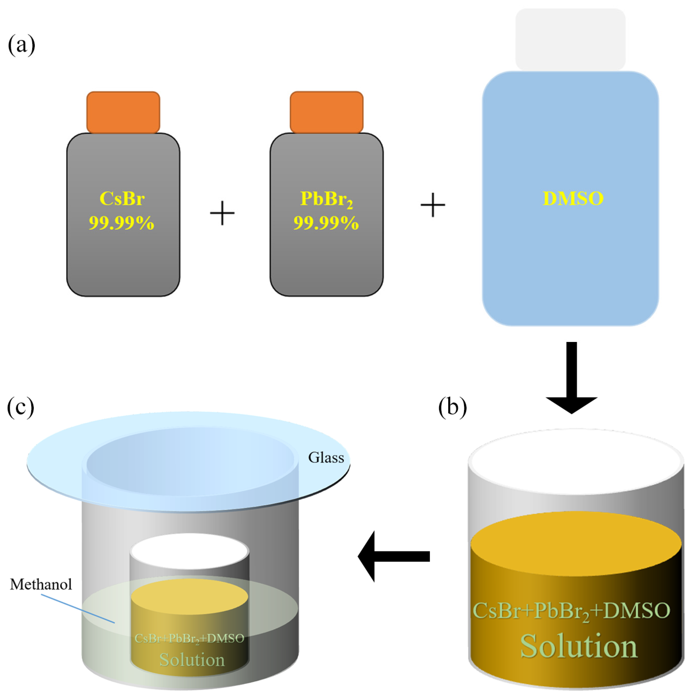
Figure 2.
(a) The room temperature XRD pattern of the CsPbBr3 single crystal; (b) the temperature-dependent XRD patterns of the CsPbBr3 single crystal.
Figure 2.
(a) The room temperature XRD pattern of the CsPbBr3 single crystal; (b) the temperature-dependent XRD patterns of the CsPbBr3 single crystal.
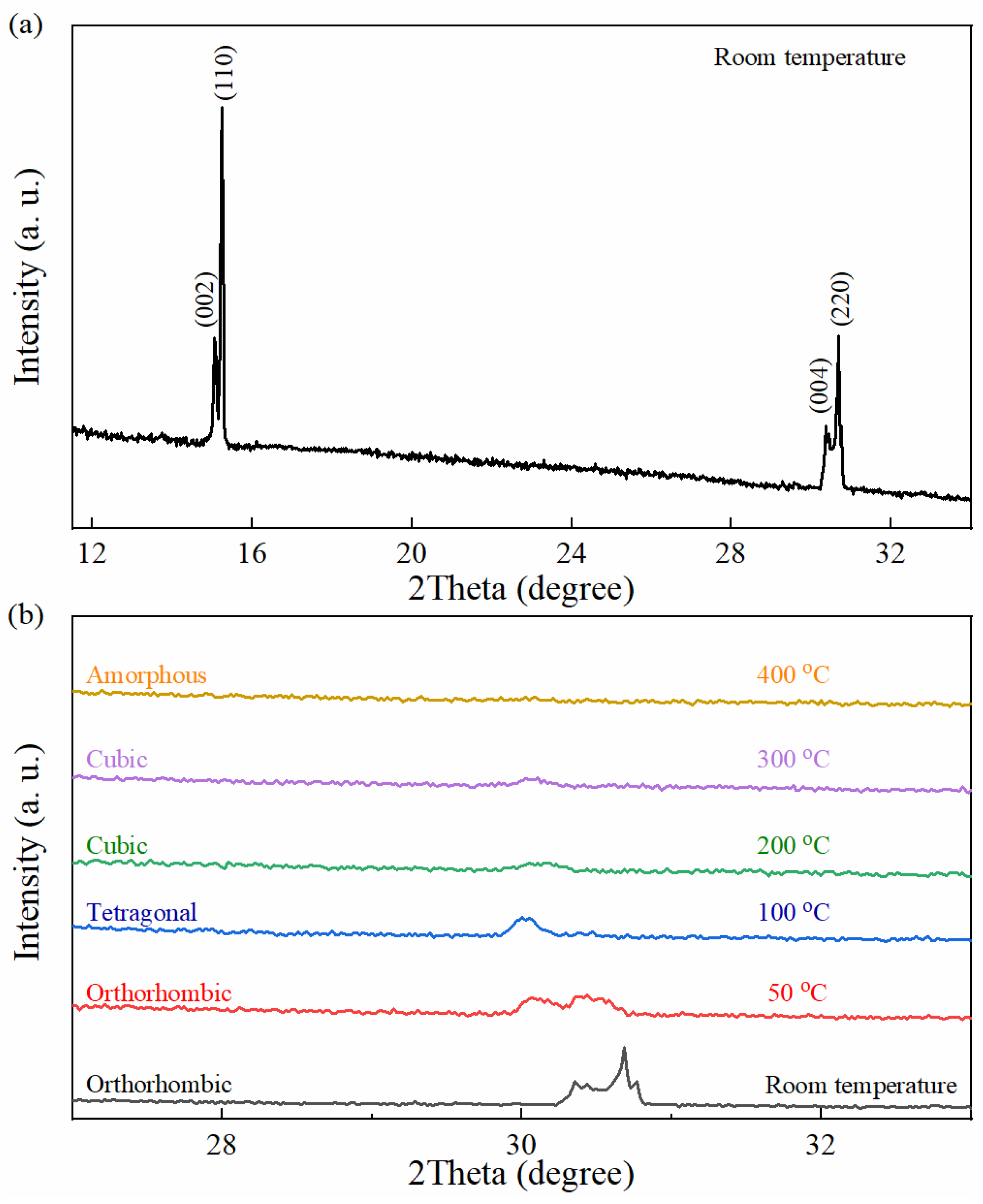
Figure 3.
The (a) PL spectrum and (b) time-resolved PL transient decay trace of the CsPbBr3 single crystal; the (c) transmittance and (d) absorption spectra of the CsPbBr3 single crystal; (e) the room temperature Raman spectrum of the CsPbBr3 single crystal excited by a 785 nm laser, and inset is the Raman spectrum measured using a 532 nm green laser; (f) the EDS spectrum of the CsPbBr3 single crystal.

Figure 4.
(a–d). The SEM images of the CsPbBr3 single crystal’s surface at different regions.
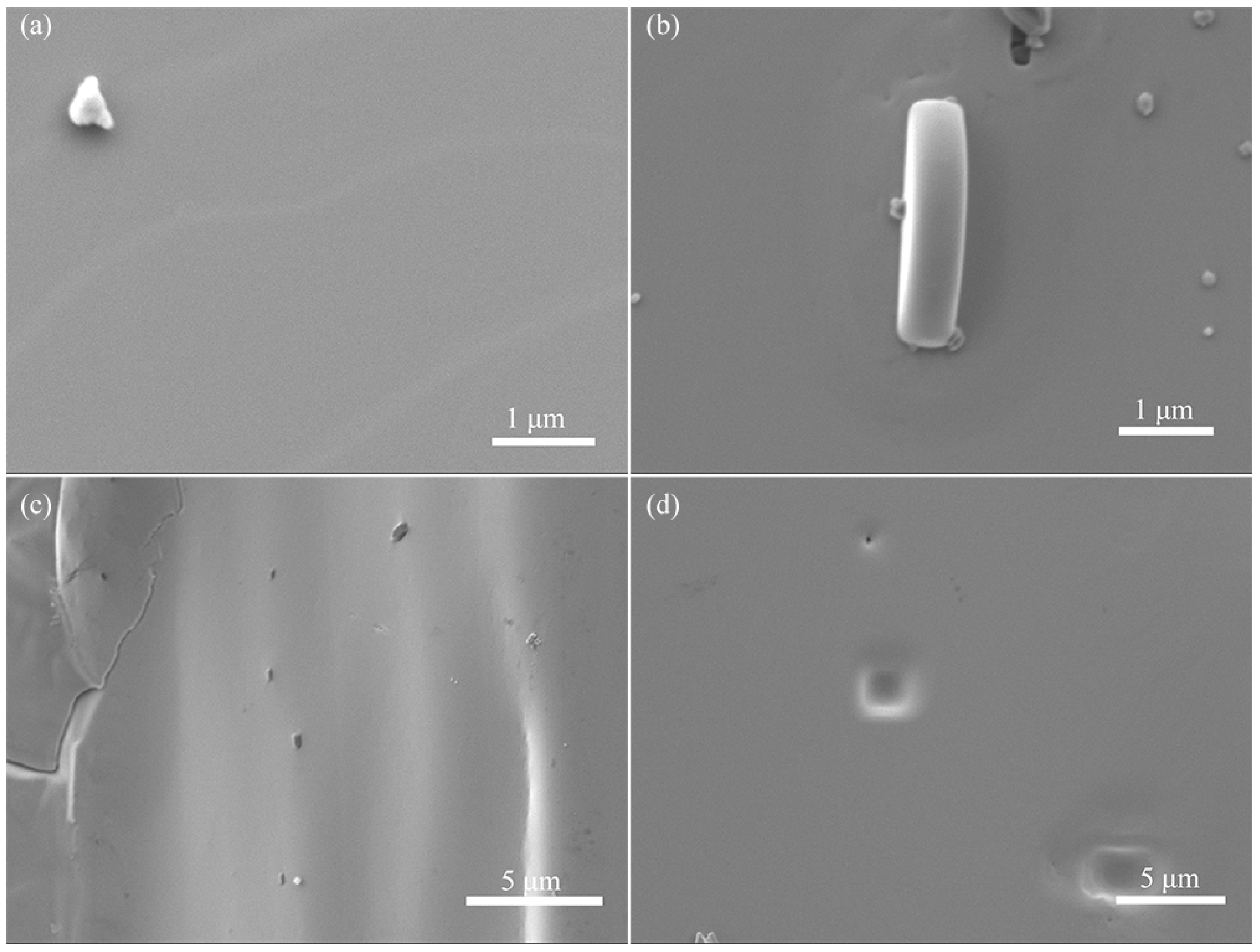
Figure 5.
(a) A regular pit shape selected for EDS mapping; (b–d) the EDS mapping of the pit’s Cs, Pb, and Br elements.
Figure 5.
(a) A regular pit shape selected for EDS mapping; (b–d) the EDS mapping of the pit’s Cs, Pb, and Br elements.

Figure 6.
(a) The I-V curve of the CsPbBr3 MSM photodetector under dark conditions; (b) the I-V curve of the CsPbBr3 MSM photodetector under dark conditions and illuminated under a 525 nm LED with different light intensities; (c) the bias voltage-dependent photocurrents of the CsPbBr3 MSM photodetector as a function of the light intensity; (d) the I-T curves of the CsPbBr3 MSM photodetector under the on–off switched illumination of 525 nm LED light with different light intensities; (e) the normalized single-cycled I-T curves of the CsPbBr3 MSM photodetector under the on–off switched illumination of 525 nm LED light with different light intensities; (f) the rise time and decay time as a function of the light intensity.
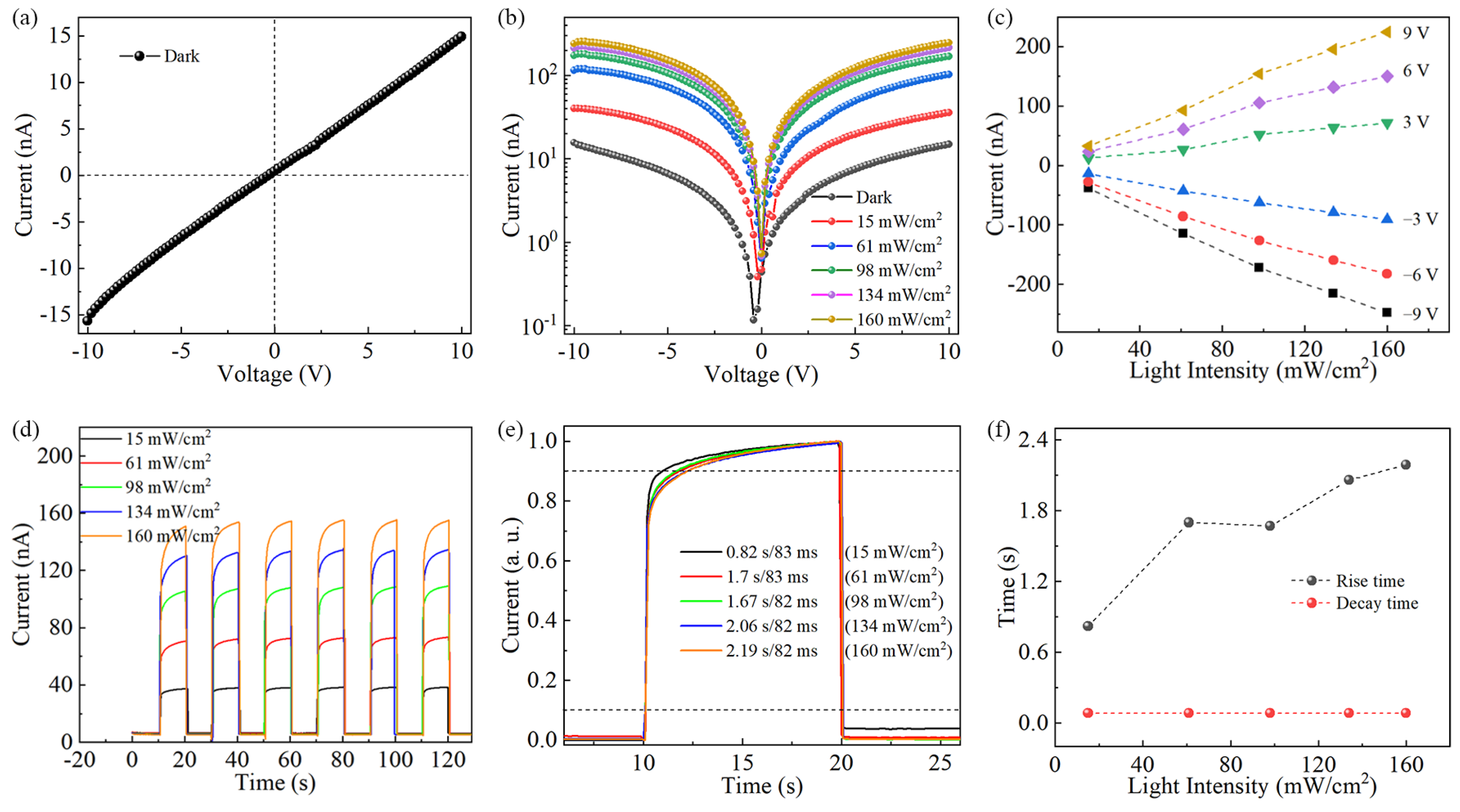
Figure 7.
The long-term I-T curves of the CsPbBr3 MSM photodetector under continuous illumination from a 525 nm green light with different light intensities.
Figure 7.
The long-term I-T curves of the CsPbBr3 MSM photodetector under continuous illumination from a 525 nm green light with different light intensities.

Disclaimer/Publisher’s Note: The statements, opinions and data contained in all publications are solely those of the individual author(s) and contributor(s) and not of MDPI and/or the editor(s). MDPI and/or the editor(s) disclaim responsibility for any injury to people or property resulting from any ideas, methods, instructions or products referred to in the content. |
© 2024 by the author. Licensee MDPI, Basel, Switzerland. This article is an open access article distributed under the terms and conditions of the Creative Commons Attribution (CC BY) license (https://creativecommons.org/licenses/by/4.0/).
Share and Cite
MDPI and ACS Style
Su, L. Growth of a Sub-Centimeter-Sized CsPbBr3 Bulk Single Crystal Using an Anti-Solvent Precipitation Method. Symmetry 2024, 16, 332. https://doi.org/10.3390/sym16030332
AMA Style
Su L. Growth of a Sub-Centimeter-Sized CsPbBr3 Bulk Single Crystal Using an Anti-Solvent Precipitation Method. Symmetry. 2024; 16(3):332. https://doi.org/10.3390/sym16030332
Chicago/Turabian StyleSu, Longxing. 2024. "Growth of a Sub-Centimeter-Sized CsPbBr3 Bulk Single Crystal Using an Anti-Solvent Precipitation Method" Symmetry 16, no. 3: 332. https://doi.org/10.3390/sym16030332
Note that from the first issue of 2016, this journal uses article numbers instead of page numbers. See further details here.