Review

Block Copolymer Nanostructures for Technology

Center for Nanoscale Materials, Argonne National Laboratory, 9700 South Cass Avenue, Argonne, IL 60439, USA
*
Author to whom correspondence should be addressed.
Polymers 2010, 2(4), 470-489; https://doi.org/10.3390/polym2040470
Submission received: 24 August 2010 / Revised: 25 September 2010 / Accepted: 15 October 2010 / Published: 20 October 2010
(This article belongs to the Special Issue Nano-Structures of Block Copolymers)

Abstract

:
Nanostructures generated from block copolymer self-assembly enable a variety of potential technological applications. In this article we review recent work and the current status of two major emerging applications of block copolymer (BCP) nanostructures: lithography for microelectronics and photovoltaics. We review the progress in BCP lithography in relation to the requirements of the semiconductor technology roadmap. For photovoltaic applications, we review the current status of the quest to generate ideal nanostructures using BCPs and directions for future research.

1. Introduction: Applications Using Block Copolymer Nanostructures

Block copolymers (BCPs), where dissimilar polymer blocks are joined by covalent bonds, draw tremendous interest for their potential applications. This is especially true for thin films of BCPs, which can be deposited inexpensively on a wide variety of substrates using solution processing techniques. The dissimilar blocks can separate into distinct domains with controllable dimensions and functionalities. The degree of long-range order and orientation of these domains can be controlled by a variety of factors, such as the interaction of the BCP molecules with the substrate, the film thickness, and the post-deposition annealing procedures [1,2]. Most studies on BCPs have focused on coil-coil diblock copolymers, where each block is a fully flexible polymer chain. Structures generated by these BCPs are well understood. For virtually all coil-coil BCPs, the various equilibrium morphologies can be completely described by a phase diagram such as that depicted in Figure 1a [3]. The self-assembled domain shapes can be tuned by adjusting the relative volume fraction of each block (f), Flory-Huggins interaction parameter χ, and the degree of polymerization N. In a typical BCP, the dimension of the domains range from 10 nm to 100 nm and can be controlled by changing the overall molecular weight of the macromolecule. BCP structures described in the phase diagram are schematically shown in Figure 1b [1]. This set of properties enables BCPs to be used as a general route for patterning a variety of materials into periodic structures. Transferring the self-assembled BCP pattern into the supporting substrate constitutes the most common example [4,5], while templating of magnetic materials [6], nanoparticles [7,8,9,10,11], and continuous thin metal films [12] have all been reported.
Figure 1. (a) Typical phase diagram of a coil-coil diblock copolymer. f: Volume fraction of one block. χ: Flory-Huggins interaction parameter. N: degree of polymerization. L: lamellae, H: hexagonally packed cylinders, Q230: double-gyroid phase, Q229: body-centered spheres, CPS: closed-packed spheres, DIS: disordered. Reprinted with permission from Reference [3]. Copyright 2006 American Chemical Society. (b) Structures of the different phases described in (a). fA is the volume fraction of block A. Reprinted from Materials Today, Vol. 13, I. Botiz and S.B. Darling, Optoelectronics using block copolymers [25]. Copyright 2010 with permission from Elsevier.
Polymers 02 00470 g001
Among the plethora of potential applications for BCPs, two topical technologies will be addressed here: microelectronic manufacturing and photovoltaic cells. The former is already approaching commercialization, whereas the latter is just beginning to show its promise. Potential for these specific applications derives primarily from the fact that BCPs are amenable to solution-based processing methods and the nanostructures they generate can be applied inexpensively and quickly over a large area. This property leads to high throughput and is fundamentally important for both cases. At present, photolithography presents a bottleneck for throughput in the microelectronics manufacturing process, and the success of any competing patterning technology would need to have a similar throughput; not all lithography techniques are suitable [13]. In this respect, BCP-based lithography holds an advantage compared to other high-resolution patterning technologies such as electron beam lithography. For wide-scale global photovoltaic applications, the cost of generating electricity from any solar cell technology needs to be equal to or less than the cost of using conventional electricity sources such as fossil fuels, and current solar panels based on silicon are too expensive and too slow to produce. Polymer-based photovoltaic cells present an inexpensive and more scalable alternative, presuming efficiency and stability requirements can be met [14].
The most important near-term application of BCPs is their use in the microelectronics industry. An impressive array of research has shown that BCPs can enhance the current capabilities of optical lithography. The dominant technology for producing fine patterns, optical lithography is fundamentally constrained by the wavelength of the light source. The microelectronics industry, the main driver of making patterns with dimensions far below the optical diffraction limit, has not reduced the wavelength of the illumination source of lithography tools to less than 193 nm since 2001, due to the difficulty of finding a suitable material for the optical elements in the lithography tools below this wavelength. In this context, templates based on block copolymers, which are high controllable, uniform and inexpensive to generate, present an attractive option to extend the semiconductor technology roadmap [15]. The magnetic recording industry has a similar impetus to make small, dense and regular patterns in magnetic materials to increase information storage density [16,17,18]. Pioneering work by Nealey et al. [19,20] and Ross et al. [21,22,23] shows the potential to generate such structures to enhance the capabilities of production-level lithography methods, by means of density multiplication.
Beyond generating fine patterns, BCPs may also be useful for photovoltaic applications. The solution-processible property of polymers is exemplified by large-area organic light-emitting diodes (OLEDs). The same property should enable large-area organic photovoltaic (OPV) cells to be produced inexpensively, although OPVs still suffer from considerable drawbacks, chiefly their low energy conversion efficiency (currently 8.13% at best [24]). In a typical OPV cell, two organic materials are present in the active layer (Figure 2), an electron donor (D) and an electron acceptor (A). The energy levels between the donor and acceptor material are offset as depicted in Figure 3 [25]. When light is absorbed in the active material, it generates bound electron-hole pairs (excitons), which are then separated at the donor-acceptor interface, leading to electric current. However, the photo-generated excitons do not diffuse further than about 10 nm before recombining. Moreover, charge carrier mobility is generally low in polymers, only on the order of 0.1 cm2/V∙s at best [26,27], and many separated charge carriers generated by solar illumination recombine before diffusing to the electrodes. Consequently, to convert light efficiently into mobile carriers, the D-A interface needs to be close to the location where the excitons are generated. At the same time, there should be a direct pathway for the separated carriers to reach the electrodes. Together, these requirements lead to the idealized design depicted in Figure 4b. The most efficient OPV cells demonstrated to date do not employ the structure shown in Figure 4b. Rather, they contain a disordered blend of the donor and acceptor materials that are phase-separated on a broadly distributed length scale. Not all photo-generated excitons are effectively separated, and the pathway to transport the separated carriers to the electrodes is convoluted and not continuous (Figure 4a). It has been proposed that employing the ideal structure in Figure 4b should improve the conversion efficiency.
Figure 2. Structure of a bilayer organic photovoltaic cell. The material used for the anode is frequently a transparent conducting oxide (TCO) on glass. Exciton separation is encouraged by using a hole-transporting layer (HTL), which serves also as an electron-blocking layer (EBL). This layer allows holes to flow to the anode but not the electrons.
Polymers 02 00470 g002
Figure 3. Schematic depiction of energy conversion in an organic photovoltaic cell. Absorption of light leads to the generation of excitons. The offset between the donor and acceptor energy levels (LUMO and HOMO) causes the excitons to separate. Reprinted from Materials Today, Vol. 13, I. Botiz and S.B. Darling, Optoelectronics using block copolymers [25]. Copyright 2010, with permission from Elsevier.
Polymers 02 00470 g003
BCPs provide a promising way to generate a structure similar to that in Figure 4b, while allowing solution-processibility at the same time. Most proposals call for using a diblock copolymer with a donor block and an acceptor block. When processed in films, the donor and the acceptor blocks form separate domains, leading to structures approaching the idealized vision. Structure-based enhancement of OPV properties has been recently demonstrated [28], although the structure was formed using nanoimprint lithography, in which case the area of the PV cell is limited by the size of the stamp and achieving a characteristic length scale of the domains comparable to the exciton diffusion distance remains a challenge. Self-assembled structures using BCPs may be more easily fabricated, thereby enabling unprecedented studies of relationships between nanostructure and photophysical properties while also being potentially amenable to roll-to-roll, truly large-scale processing.
Figure 4. (a) Commonly depicted morphology of a bulk heterojunction OPV cell with disordered and discontinuous charge transport networks. Blue: acceptor domains. Red: donor domains. (b) Commonly proposed ideal morphology for an OPV cell. Blue: acceptor domains. Red: donor domains. The width of each domain is comparable to the exciton diffusion length and the active layer thickness is sufficient to absorb the incident sunlight.
Polymers 02 00470 g004
In this review, we examine BCP-based nanostructures in the context of these two important applications: lithography for the microelectronics industry and solar energy conversion. Specifically, we examine the achievements and remaining challenges associated with BCPs in making high resolution patterns for the microelectronic industry. We review as well the applications of BCPs in photovoltaics, the current status of polymer assembly, the achieved energy conversion efficiency, and future directions of research. As related reviews exist in each of these areas, here we focus only on some key recent developments.

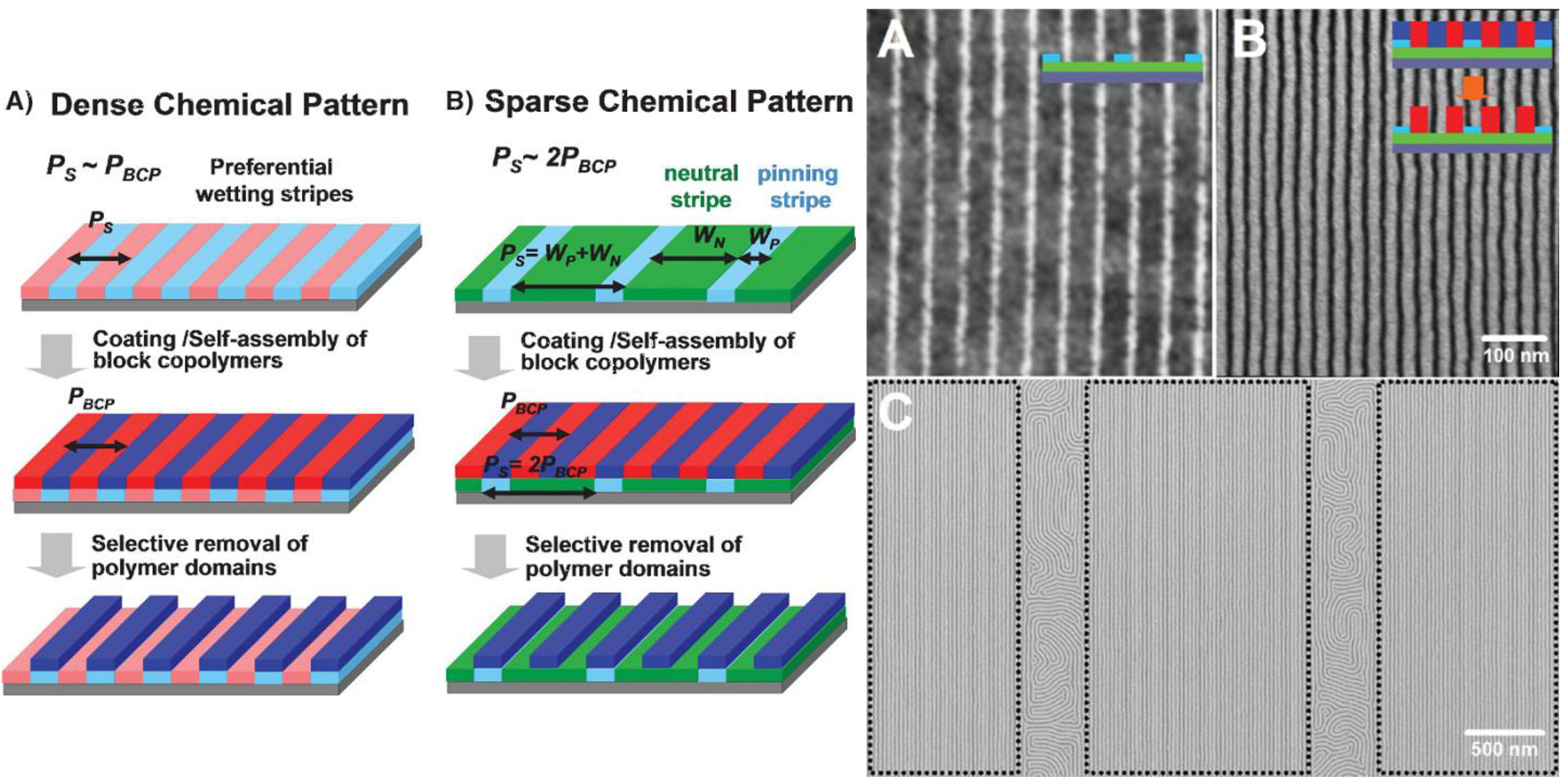
2. Current Status of Density Multiplication Using Guided Assembly of Block Copolymers

Optical lithography has been enormously successful in making fine patterns. Over a span of four decades, this technology has met the microelectronic industry’s demand for resolution, uniformity, throughput, multi-layer registry and cost. The reduction of the illumination source’s wavelength has largely enforced Moore’s law for over 40 years. However, there are fundamental difficulties with further reducing the wavelength of the illumination source. Instead, working with an illumination wavelength of 193 nm, lithography engineers in the semiconductor industry employ sophisticated techniques, such as phase-shifting masks [29], immersion lithography [30,31], and increasingly, double-exposure methods [32] to meet the resolution requirements of the semiconductor technology roadmap.
BCPs can further advance optical lithography by ways of density multiplication. This is achieved by making BCP self-assemble on a pre-patterned substrate, as first demonstrated by Rockford et al. [33]. The patterns provide either topographical or chemical constraints that guide the assembly of the BCP domains and can be of much larger dimensions than the domains of the BCP. In general, they need to be an integer multiple of the period of the BCP structure, or commensurate, to generate defect-free patterns.
Nealey’s group has done extensive work in assembling BCPs on surfaces with chemically modified patterns, showing the possibility of replicating faithfully the underlying patterns [34]. Using chemical contrast between SiO2 and hydroxyl-terminated polystyrene, ordered poly(styrene-block-methyl methacrylate) (PS-b-PMMA) domains can be formed, with long-range ordering and a four-fold density multiplication [9]. Work from Cheng et al. [35] introduced the concept of inducing density multiplication by using a neutral surface to both BCP blocks, with constraints provided by chemical modification (Figure 5) [35]. Guided assembly of BCPs is sufficiently flexible to generate fairly complicated patterns that occur frequently in integrated circuits (Figure 6) [20,36], and beyond the periodic BCP patterns predicted by the phase diagram in Figure 1b. A substantial body of work has shown the possibility to constrain and order BCPs, especially PS-b-PMMA, using topographical features. However, to generate a truly periodic pattern over a large area using density multiplication, the guiding pattern needs to have the same orientation as the BCP domains (i.e., posts to guide out-of-plane cylinders, trenches to guide lamellae or in-plane cylinders). This requires the thickness of the BCP layer to be appropriate for the desired patterns, and precise thickness control is critical [37]. Nevertheless, high density multiplying factor can be achieved, as exemplified by Tada et al., where the density can be increased up to nine times [16] using pre-patterned and etched surfaces. By exploiting the effect of commensurability, recent work by Yang et al. [38] demonstrates the possibility of generating complex patterns in poly(styrene-block-dimethylsiloxane) (PS-b-PDMS) using only a sparse guiding pattern.
It has been consistently shown that guided self-assembly of BCPs is robust with respect to the imperfections in the underlying pattern. As an example, work by Tada et al. [17] clearly shows that order in the BCP film can be immune to defects in substrate topography, and that the commensurability of the guiding pattern has the strongest effect on the final BCP lateral order. BCP domains are also immune to non-idealities in the lithographic process, such as line-edge roughness (LER) in the topography [39] and even broken lines [35].
Even without using a guiding substrate, BCP domains can be ordered over a fairly large area [40,41]. Most experimental characterization of BCP structures relies on AFM imaging, a technique suitable for only relatively small area. Methods more applicable to large area examination such as Moiré patterns, GISAXS measurements, and SEM image-based orientation correlation have been demonstrated by Park et al. [42], and show that lateral order over 10 μm is possible.
The range of ordering can be greatly enhanced by the pattern of the underlying substrate [43,44,45] without interrupting the polymer lattice. Park et al. used a textured sapphire surface in combination with solvent annealing to generate perfect ordering of PS-b-PEO over an area of 4 cm2 [46]. Recent work by Jung et al. [47] also shows that, in a lithography-guided assembly, the uniformity in the lateral ordering can be extended over an area of several cm2.
Figure 5. Density multiplication and directed assembly using chemical patterns. E-beam lithography defines sparse pinning stripes. (Left) Comparison of schemes for directing BCP self-assembly. Scheme B) was used to induce density multiplication. (Right) A) shows the sparse e-beam resist lines defining the pinning stripes. B: resulting PS-b-PMMA pattern showing density multiplication. Reprinted with permission from Reference [35]. Copyright 2008, Wiley-VCH.
Polymers 02 00470 g005
Figure 6. Common lithographic patterns for microelectronics and realization of some of the geometries using block copolymer self-assembly. Reprinted with permission from Reference [36]. Copyright 2007 American Chemical Society.
Polymers 02 00470 g006

3. Some Challenges and Potential Limitations of BCP Lithography

3.1. Pattern Transfer

Patterns generated using any lithography technique are usually transferred to the underlying materials using etching processes. For very small features, dry etching processes such as reactive ion etching (RIE) or ion milling are the only methods capable of transferring them faithfully. Since the polymer blocks in most BCPs are based on carbon, the etch selectivity between the blocks is generally poor in technologically relevant RIE gases. In the most commonly studied BCP for lithography, PS-b-PMMA, the etch rate of PMMA blocks is only about twice that of PS for most RIE gases [48]. A BCP film used for lithography is typically thinner than 50 nm because of the critical dependence of the film morphology on the thickness, and is therefore too thin to withstand the etching process. Only a few polymer blocks have shown promising etch resistance, and most pattern transfer processes following BCP lithography necessitate a hard mask. Polymer blocks containing metals such as polyferrocenylsilanes (PFS) [49,50,51,52] or silicon such as PDMS [53,54,55] have enhanced resistance to plasma etching, and therefore a large etch contrast relative to organic blocks. However, since iron degrades transistor performance, its presence in semiconductor processing is generally undesirable, especially for front-end processes where the high-resolution capability of BCP lithography is most relevant.

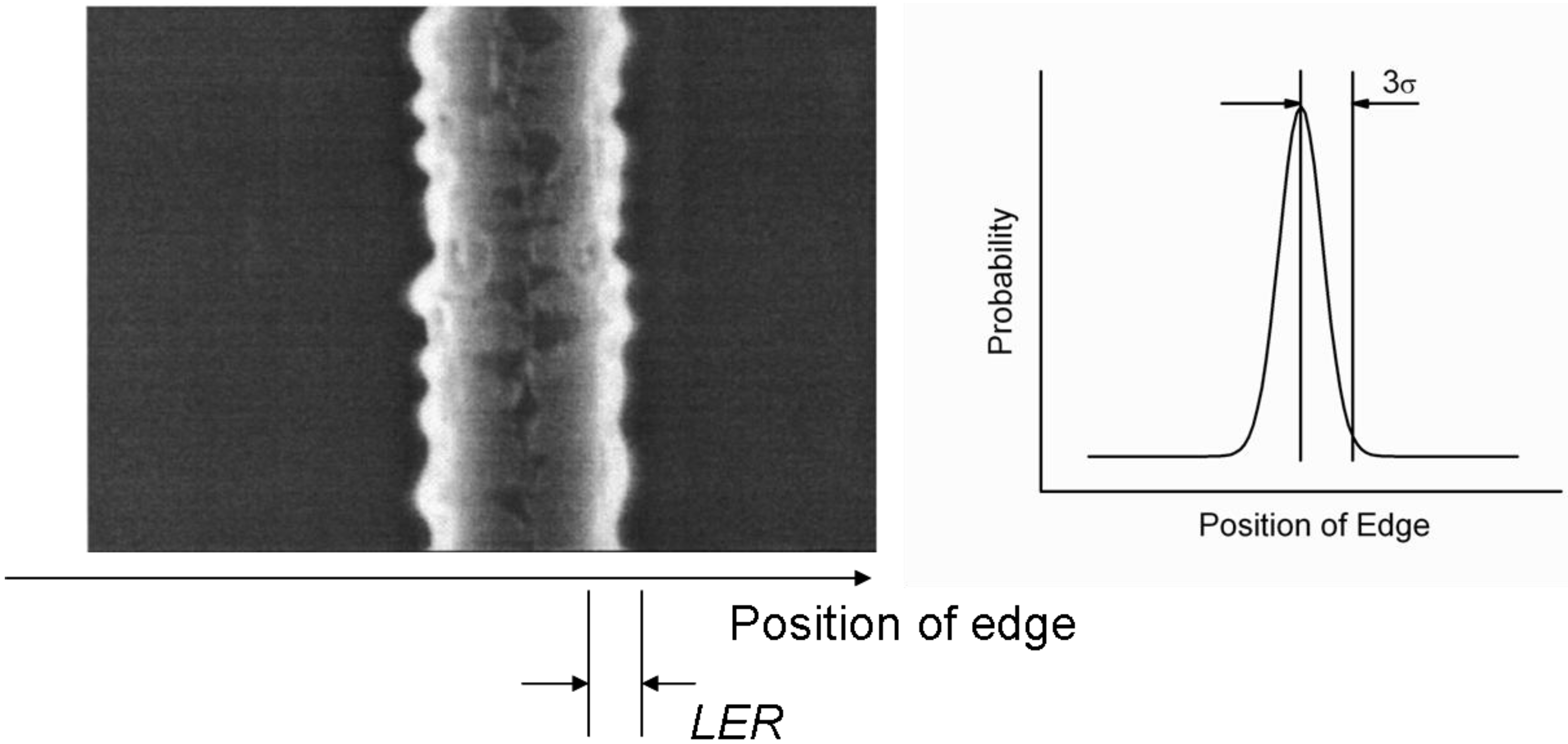
3.2. Line-Edge Roughness

As mentioned in the Introduction, optical lithography has been successfully applied for microelectronics manufacturing because it satisfies many stringent requirements of the industry. Achieving high resolution is only one of the many requirements. For future technology nodes, the industry also needs better quality in the lithographic pattern, quantified namely by the line-edge roughness (LER) of a printed line in the photoresist (Figure 7) [56]. This roughness, if transferred into the smallest printed feature, which corresponds usually to the gate length of a transistor, can change the performance of the device significantly and in a complex manner. For an integrated circuit containing more than one billion such transistors, the results are mostly negative. Some consequences are: increased transistor leakage [57] (large stand-by power consumption), spread in threshold voltage [58] (decreased distinction between the digital 1s and 0s), and reduced read/write margin in a memory cell [59]. As a result, the requirements on LER are stringent, being 3σ < 1.4 nm for technology nodes more advanced than 22 nm [13].
Guided BCP assembly can reduce LER of the guiding pattern [23], although the studies performed to date began with exaggerated roughness, and it is not clear whether BCPs can improve on the currently achievable LER using optical lithography. In fact, the BCP lithography community has yet to demonstrate a solution that meets the industry’s requirement on LER. Intrinsic roughness of each BCP domain is the limiting factor, which arises from a non-vanishing interface width between two dissimilar domains (Figure 8). Simulation studies [60] suggest that increasing the Flory-Huggins parameter χ is the most direct way to reduce LER, since the interface width between the blocks is proportional to χ −1/2 [61]. Highly dissimilar blocks such as PS and PDMS (χ = 0.26) should improve considerably the edge sharpness of the domains [62], although there is a dearth of confirming reports. The LER also depends on the degree of polymerization N of each block, with larger N leading to smoother lines [63]. However, this is at odds with achieving high spatial resolution using small domain sizes, which would require low-molecular weight blocks. The optimization of LER is only beginning, and experimental results on quantification and reduction of the LER in BCP patterns are unfortunately still lacking. Recent measurement using soft x-ray diffraction [64] seems to provide a general pathway in characterizing this important parameter, although the reported quantity, 3σ~4.9 nm, is large for industrial lithographic purposes.
Figure 7. Definition of line edge roughness (LER). A normal distribution (right) of the line edge position is compiled from an SEM image (left), and LER is defined as 3 × the standard deviation σ. SEM image was reprinted with permission from Reference [56]. Copyright 1999, American Vacuum Society.
Polymers 02 00470 g007
Figure 8. Illustration of ξ, the interface width between two polymer domains. f: volume fraction of each polymer block. Block A and B are randomly mixed inside the interface region.
Polymers 02 00470 g008

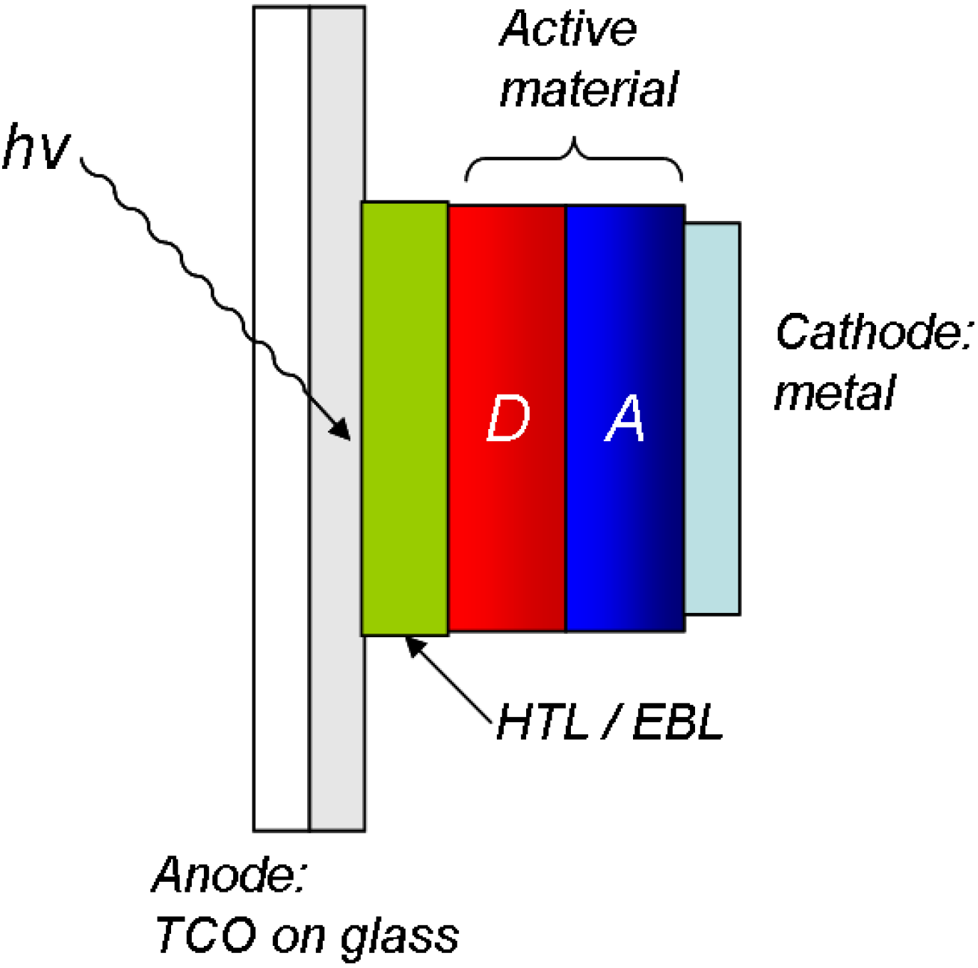
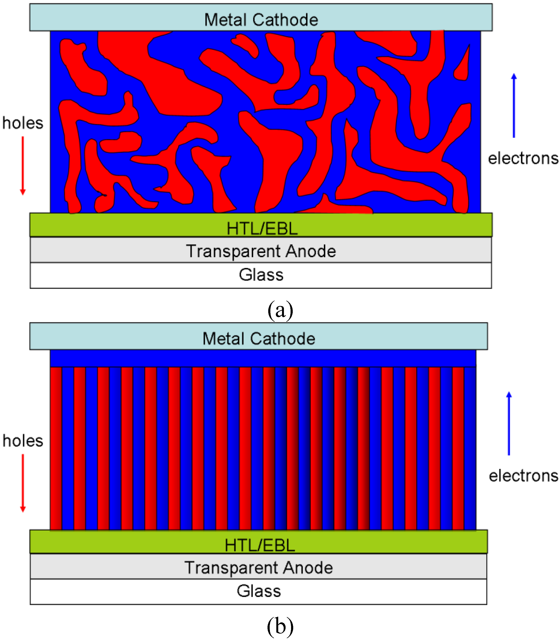
4. Requirements on the Nanostructure of Conjugated BCPs for Photovoltaic Purposes

Another emerging technological application of BCPs is their use in photovoltaic cells. The justification for applying BCPs to photovoltaics was explained in the Introduction, and much of the work was reviewed recently [25,65,66]. The polymers used for photovoltaic applications usually have a conjugated backbone on which the molecular orbitals are delocalized. This leads to an energy gap that matches parts of the solar spectrum, generally towards the bluer wavelengths for commonly studied materials. The rigid, conjugated backbone leads to different phase-separation behavior from the more frequently studied coil-coil BCPs. Conjugated blocks are often described as “rods” since they are rigid compared to more flexible coil blocks. Rod-coil BCPs form various kinds of lamellar phases [67] depending on the relative fraction of the rod. These phases are better described using the theory for liquid crystals, especially in the limit where the coil block constitutes only a small volume fraction. Olsen et al. [68,69] used a variety of techniques, including x-ray diffraction and optical transmission, to map out the phase diagram of a poly(phenylenevinylene-block-isoprene) PPV-b-PI rod-coil polymer.
For photovoltaic applications, the domain sizes need to match approximately the exciton diffusion length (~10 nm). Since the rod blocks are substantially dissimilar from the coil blocks, due to the stiffness of the rods, conjugated BCPs can easily separate into small (<10 nm) domains [67]. Because the conjugated blocks are rigid, it is not necessary to have a large block to form lamellar domains with width smaller than 10 nm. This is in contrast to coil-coil BCPs where a larger minimum degree of polymerization N is required to produce phase separation. Thus, for making the idealized OPV structure illustrated in Figure 4b, rod-coil BCPs can satisfy the requirements in dimension and structure. The spacing between the conjugated blocks, defined by the coil block, is also important, since this determines the dimensions of the other phase. This parameter can also be controlled, and it was shown by Tao et al. [70] that adding rod homopolymer to the BCP can change the spacing between the lamellar domains.
Detailed requirements on the conjugated BCP structure for PV purposes are, however, not limited to the size and orientation of the domains. Numerical simulation by Shah [71] shows that the anisotropic mobility in the polymer and a non-vanishing interface width between the donor/acceptor domains can both strongly influence the conversion efficiency (Figure 9) [71]. The interface between the rod phase and the coil phase can be sharp, but only at high rod fractions [72], and there is a paucity of measurements on the interface quality. Additionally, the ideal OPV structure depicted in Figure 4b can be realized only if the lamellae of the rod blocks align normally to the substrate. For a film that is thick enough to absorb a significant amount of light, this means that the lamellae of length comparable to the film thickness need to align normally to the substrate. In thick films of rod-coil BCPs, this is not always the case. Studies by Olsen et al. [73,74] on PPV-b-PI show that the orientation of the lamellae depends strongly on the affinity of the blocks to the substrate surface, and that the mutual alignment of the ”grains” of lamellae becomes poor at large film thicknesses (Figure 10) [74]. This is analogous to coil-coil BCPs, where the orientation of (for example) cylindrical domains is influenced strongly by the substrate surface and the film thickness. In the context of making efficient OPV cells, the orientation of the lamellae is critical. Using a brush layer that presents a neutral surface to both blocks may help, although it would have to be a good conductor at the same time. Other ordering techniques, such as using magnetic fields [75] may also be adequate.
Figure 9. Calculated short-circuit current density Jsc (mA/cm2) in an OPV cell vs. the interface width ξ (nm) between the donor and acceptor domain. The assumed structure contains donor and acceptor domains perpendicular to the plane of electrode. Reprinted with permission from Reference [71]. Copyright 2010 American Chemical Society.
Polymers 02 00470 g009
Figure 10. (Left) Cross-sectional TEM image of a rod-coil BCP film of PPV-b-PI. (Right) Schematic of morphology of a rod-coil BCP film as a function of film thickness. Reproduced with permission from Reference [74]. The Royal Society of Chemistry. Hyperlink: http://dx.doi.org/10.1039/B809092K.
Polymers 02 00470 g010

5. Current Progress Using Donor-Acceptor BCPs

The highest-efficiency OPV cell reported to date is a homogeneous blend of electron-donating and -accepting materials without an ordered, continuous pathway for charge extraction. It does not guarantee uniform D/A interfaces for exciton separation throughout the active layer volume either. Phase separation of a copolymer consisting of a donor block and an acceptor block may be a straightforward way to generate an ideal OPV morphology. Reported energy conversion efficiencies using this approach have not been high: Hazdiioannou’s group has several reports on synthesizing BCPs containing PPV and C60, with the latter grafted onto polystyrene [76]. A small photovoltaic effect under monochromatic illumination was demonstrated [77]. Similar work using a poly(3-hexylthiophene) (P3HT) donor block and C60-grafted PMMA [78] shows improved photoluminescence quenching compared to a simple blend of P3HT and phenyl-C61-butyric acid methyl ester (PCBM), indicating better exciton dissociation, although photovoltaic cells made from such material demonstrated only a modest photovoltaic effect. Recent work by Tao et al. [79] using P3HT as the donor and perylene as the acceptor, and by King et al. [80] using PvTPA-perylene, also demonstrate phase separation of the blocks, although the PV effect is decidedly modest in both cases. Zhang et al. [72] synthesized a P3HT-b-perylene diimide acrylate (P3HT-b-PPDA) block copolymer, taking advantage of the high carrier mobility in both phases. The films show complete PL quenching and the PV device shows a respectable conversion of efficiency of 0.49%, although no clear relationship was established between the structure of the film and the efficiency, since the device was fabricated on an as-spun thin film that did not show the same structure as a post-annealed film. A recent report validates this approach, however, by showing a significant increase in efficiency in an inverted device structure, using poly(3-hexylthiophene-block-4-vinyl pyridine) P3HT-b-P4VP copolymer, with PCBM acceptor grafted to the P4VP blocks [81].
While the donor-acceptor diblock copolymer methodology can enable fabrication of the ideal OPV structure, the covalent link between these two blocks may also lead to rapid charge carrier recombination. Several recent reports have examined the use of a spacer or “bridge” block between the donor and the acceptor to improve PV device performance. The demonstration by Sun [70] using PPV-based blocks shows that this approach can significantly improve the open-circuit voltage, although the photocurrent is low. Nevertheless, photoluminescence quenching is observed [82]. A similar attempt was made using polycarbazole (PCz) donors and perylenetetracarboxydiimide (PDI) acceptor with a saturated spacer [83], but a conversion efficiency of only 0.004% was demonstrated. Phase separation in a P3HT-b-PS-b-(PS/C60) triblock copolymer, with ungrafted PS chains as spacer, has also been reported [84], although no device performance was presented.
Another approach to fabricate the structure in Figure 4b would be a multi-step process that employs a rod-coil BCP containing only the donor (rod) phase, and a coil block that can be removed after phase separation. The coil block can be etched and the space refilled with the acceptor material. Botiz et al.[85] and Boudouris et al.[86] both demonstrated the possibility of generating structures in poly(3-hexylthiophene-block-lactide) (P3HT-b-PLA) by the removal of the PLA domains, with the former work also showing subsequent re-filling using fullerene acceptors and concomitant PL quenching. The wet procedures used to etch the PLA blocks introduce the problem of pattern collapse [87], which commonly occurs in the fabrication of high-aspect ratio nanostructures. A three-dimensional structure, such as that generated using the gyroid phase [88] as in Figure 1b, may provide the structural rigidity that allows the pattern to withstand the capillary forces encountered during the fabrication procedures, although the pathway for charge carrier transport is less direct.
So far, donor-acceptor BCPs appear to have the most positive impact on OPV devices when they are used as a “compatibilizer”, or surfactant to facilitate the blending of the donor and acceptor materials. The addition of BCP to PV devices containing P3HT and fullerenes improves the initial energy conversion efficiency of bulk heterojunction devices [89], and also significantly enhances their thermal stability [90,91,92]. Under prolonged thermal annealing, the addition of BCP prevents the macroscopic aggregation of P3HT and fullerenes [91,92]. This preserves the large exciton dissociation interface in a bulk heterojunction structure that is responsible for the high energy conversion efficiency. In a blend of polythiophene and polyquinoline, previously shown to have significant PL quenching [93], the improvement on morphology is also demonstrated [94], where the addition of the copolymer strongly reduces macroscopic phase separation.

6. Summary and Future Directions

There is enough knowledge on block copolymer synthesis and assembly to warrant serious consideration for important technological applications. For lithography, BCPs can provide uniform and small feature size, long-range order, robust etch resistance, and can generate diverse patterns. For photovoltaic applications, BCP self-assembly is a promising way to create, over a large area, nanoscopically ordered structure of functional materials with dimensions suitable for efficient extraction of photo-generated carriers.
Overcoming the remaining challenges in BCP lithography for industrial purposes requires engineering on the molecular level. Very dissimilar blocks that have large Flory-Huggins parameter would facilitate phase segregation for small molecules (enhancing resolution) and improve on the LER. By incorporating inorganic components, these blocks would also conceivably have larger etch contrast. Indeed, recent research on BCP lithography using polystyrene-block-polyethyleneoxide (PS-b-PEO) [95,96,97] shows the possibility of making dense sub-10 nm features, dimensions that are difficult to produce even for electron-beam lithography. Methods such as multi-layer BCPs [47], and inorganic polymer blocks containing polyhedral oligomeric silsesquioxane (POSS) [98] have also clearly demonstrated sub-10 nm feature sizes.
As to improving pattern transfer, polymer blocks containing inorganic blocks, such as PDMS, or the recently-reported POSS, can significantly enhance the etch contrast. Other issues concerning pattern transfer include the detailed three-dimensional geometry of the pattern. In photolithographically generated photoresist features, the side-wall profile strongly influences the final dimensions and geometry of the transferred pattern, and it is generally desired to have straight side walls that are perpendicular to the substrate plane. In diblock copolymer lithography, the side-wall angle is not independently controllable from the shape of the domains. In-plane cylinders have curved walls and would not do well for transferring the patterns vertically. Although out-of-plane cylinders and lamellar domains have vertical side walls, using these phases exclusively would place additional restriction the design of the polymer.
Beyond the challenging synthetic chemistry needed to make BCPs with functional blocks suitable for PV applications, many issues need to be resolved before BCPs can be a viable route for producing useful PV cells. Controlling the film morphology, such that the polymer domains orient perpendicularly to the substrate plane, stands out as a basic problem to be solved. This is analogous to the case of coil-coil BCPs used in lithography, where the domain orientation can be controlled by manipulating the boundary conditions of the BCP film. The interface sharpness between the blocks is also a fundamental obstacle, since it may limit the exciton separation efficiency. This is also a fundamental problem for BCP lithography.
Many of the challenges in improving the optoelectronic properties of BCPs are the same as those in organic optoelectronic devices in general. Organic PV materials usually absorb higher energy photons because of a large HOMO-LUMO gap. Since the optimal band-gap energy for all PV materials is about 1.4 eV [99], lowering the HOMO-LUMO gap is generally desired. Reducing the optical gap would also imply stronger optical absorption from a thinner film, and controlling the morphology of a thinner film using boundary conditions may be easier. Moreover, carrier mobility is generally low in organic semiconductors, leading to small exciton diffusion length. Improving carrier mobility would relax many requirements on the BCP geometry, especially the size of the domains. Nevertheless, despite these challenges, the fundamental advantage of BCPs—the possibility for inexpensive large-scale deployment remains a valid and compelling motivation for further research.

Acknowledgements

Use of the Center for Nanoscale Materials was supported by the U.S. Department of Energy, Office of Science, Office of Basic Energy Sciences, under Contract No. DE-AC02-06CH11357.

References

  1. Darling, S.B. Directing the self-assembly of block copolymers. Progr. Polym. Sci. 2007, 32, 1152–1204. [Google Scholar] [CrossRef]
  2. Kim, H.C.; Park, S.M.; Hinsberg, W.D. Block copolymer based nanostructures: Materials, processes, and applications to electronics. Chem. Rev. 2010, 110, 146–177. [Google Scholar] [CrossRef] [PubMed]
  3. Cochran, E.W.; Garcia-Cervera, C.J.; Fredrickson, G.H. Stability of the gyroid phase in diblock copolymers at strong segregation. Macromolecules 2006, 39, 2449–2451. [Google Scholar] [CrossRef]
  4. Guarini, K.W.; Black, C.T.; Zhang, Y.; Kim, H.; Sikorski, E.M.; Babich, I.V. Process integration of self-assembled polymer templates into silicon nanofabrication. J. Vac. Sci. Technol. B 2002, 20, 2788–2792. [Google Scholar] [CrossRef]
  5. Black, C.T.; Ruiz, R.; Breyta, G.; Cheng, J.Y.; Colburn, M.E.; Guarini, K.W.; Kim, H.C.; Zhang, Y. Polymer self assembly in semiconductor microelectronics. IBM J. Res. Dev. 2007, 51, 605–633. [Google Scholar] [CrossRef]
  6. Hamley, I.W. Nanostructure fabrication using block copolymers. Nano Technol. 2003, 14, R39–R54. [Google Scholar]
  7. Aizawa, M.; Buriak, J.M. Block copolymer templated chemistry for the formation of metallic nanoparticle arrays on semiconductor surfaces. Chem. Mater. 2007, 19, 5090–5101. [Google Scholar] [CrossRef]
  8. Shenhar, R.; Norsten, T.B.; Rotello, V.M. Polymer-mediated nanoparticle assembly: Structural control and applications. Adv. Mater. 2005, 17, 657–669. [Google Scholar] [CrossRef]
  9. Darling, S.B. Mechanism for hierarchical self-assembly of nanoparticles on scaffolds derived from block copolymers. Surf. Sci. 2007, 601, 2555–2561. [Google Scholar] [CrossRef]
  10. Darling, S.B.; Hoffmann, A. Tuning metal surface diffusion on diblock copolymer films. J. Vac. Sci. Technol. A 2007, 25, 1048–1051. [Google Scholar] [CrossRef]
  11. Lopes, W.A.; Jaeger, H.M. Hierarchical self-assembly of metal nanostructures on diblock copolymer scaffolds. Nature 2001, 414, 735–738. [Google Scholar] [CrossRef] [PubMed]
  12. Park, S.; Kim, B.; Cirpan, A.; Russell, T.P. Preparation of metallic line patterns from functional block copolymers. Small 2009, 5, 1343–1348. [Google Scholar] [CrossRef] [PubMed]
  13. The International Technology Roadmap for Semiconductors. Available online: http://www.itrs.net (accessed on 18 October 2010).
  14. Krebs, F. Polymeric Solar Cells: Materials, Design, Manufacture, 1st ed.; DEStech Publications, Inc.: Lancaster, PA, USA, 2010; pp. 119–169. [Google Scholar]
  15. Craig, G.S.W.; Nealey, P.F. Directed assembly of block copolymers on lithographically defined surfaces. Proc. SPIE 2010, 7637, 76370L. [Google Scholar]
  16. Tada, Y.; Akasaka, S.; Takenaka, M.; Yoshida, H.; Ruiz, R.; Dobisz, E.; Hasegawa, H. Nine-fold density multiplication of hcp lattice pattern by directed self-assembly of block copolymer. Polymer 2009, 50, 4250–4256. [Google Scholar] [CrossRef]
  17. Tada, Y.; Akasaka, S.; Yoshida, H.; Hasegawa, H.; Dobisz, E.; Kercher, D.; Takenaka, M. Directed self-assembly of diblock copolymer thin films on chemically-patterned substrates for defect-free nano-patterning. Macromolecules 2008, 41, 9267–9276. [Google Scholar] [CrossRef]
  18. Tada, Y.; Akasaka, S.; Chen, F.; Yoshida, H.; Takenaka, M.; Hasegawa, H. Density multiplication by directed self-assembly of block copolymer binary blends. J. Photopolym. Sci. Technol. 2009, 22, 229–233. [Google Scholar] [CrossRef]
  19. Ruiz, R.; Kang, H.M.; Detcheverry, F.A.; Dobisz, E.; Kercher, D.S.; Albrecht, T.R.; de Pablo, J.J.; Nealey, P.F. Density multiplication and improved lithography by directed block copolymer assembly. Science 2008, 321, 936–939. [Google Scholar] [CrossRef] [PubMed]
  20. Liu, G.L.; Thomas, C.S.; Craig, G.S.W.; Nealey, P.F. Integration of density multiplication in the formation of device-oriented structures by directed assembly of block copolymer-homopolymer blends. Adv. Funct. Mater. 2010, 20, 1251–1257. [Google Scholar] [CrossRef]
  21. Cheng, J.Y.; Ross, C.A.; Chan, V.Z.H.; Thomas, E.L.; Lammertink, R.G.H.; Vancso, G.J. Formation of a cobalt magnetic dot array via block copolymer lithography. Adv. Mater. 2001, 13, 1174–1178. [Google Scholar] [CrossRef]
  22. Ross, C.A.; Smith, H.I.; Savas, T.; Schattenburg, M.; Farhoud, M.; Hwang, M.; Walsh, M.; Abraham, M.C.; Ram, R.J. Fabrication of patterned media for high density magnetic storage. J. Vac. Sci. Technol. B 1999, 17, 3168–3176. [Google Scholar] [CrossRef]
  23. Bita, I.; Yang, J.K.W.; Jung, Y.S.; Ross, C.A.; Thomas, E.L.; Berggren, K.K. Graphoepitaxy of self-assembled block copolymers on two-dimensional periodic patterned templates. Science 2008, 321, 939–943. [Google Scholar] [CrossRef] [PubMed]
  24. Solarmer Energy, Inc. Available online: http://www.solarmer.com (accessed on 18 October 2010).
  25. Botiz, I.; Darling, S.B. Optoelectronics using block copolymers. Mater. Today 2010, 13, 42–51. [Google Scholar] [CrossRef]
  26. Sirringhaus, H.; Brown, P.J.; Friend, R.H.; Nielsen, M.M.; Bechgaard, K.; Langeveld-Voss, B.M.W.; Spiering, A.J.H.; Janssen, R.A.J.; Meijer, E.W.; Herwig, P.; de Leeuw, D.M. Two-dimensional charge transport in self-organized, high-mobility conjugated polymers. Nature 1999, 401, 685–688. [Google Scholar] [CrossRef]
  27. Horowitz, G. Organic field-effect transistors. Adv. Mater. 1998, 10, 365–377. [Google Scholar] [CrossRef]
  28. He, X.M.; Gao, F.; Tu, G.L.; Hasko, D.; Huttner, S.; Steiner, U.; Greenham, N.C.; Friend, R.H.; Huck, W.T.S. Formation of nanopatterned polymer blends in photovoltaic devices. Nano Lett. 2010, 10, 1302–1307. [Google Scholar] [CrossRef] [PubMed]
  29. Levenson, M.D.; Viswanathan, N.S.; Simpson, R.A. Improving resolution in photolithography with a phase-shifting mask. IEEE Trans. Electron. Devices 1982, 29, 1828–1836. [Google Scholar] [CrossRef]
  30. Hinsberg, W.; Wallraff, G.; Larson, C.; Davis, B.; Deline, V.; Raoux, S.; Miller, D.; Houle, F.; Hoffnagle, J.; Sanchez, M.; Rettner, C.; Sundberg, L.; Medeiros, D.; Dammel, R.; Conley, W. Liquid immersion lithography––Evaluation of resist issues. In Liquid immersion lithography––Evaluation of Resist Issues; Sturtevant, J.L., Ed.; SPIE-International Society Optical Engineering: Bellingham, WA, USA, 2004; pp. 21–33. [Google Scholar]
  31. Lin, B.J. Immersion lithography and its impact on semiconductor manufacturing. In Immersion Lithography and its Impact on Semiconductor Manufacturing, 1st ed.; Smith, B.W., Ed.; SPIE-International Society Optical Engineering: Bellingham, WA, USA, 2004; pp. 46–67. [Google Scholar]
  32. Byers, J.; Lee, S.; Jeri, K.; Zimmerman, P.; Turr, N.J.; Willson, C.G. Double exposure materials: Simulation study of feasibility. J. Photopolym. Sci. Technol. 2007, 20, 707–717. [Google Scholar] [CrossRef]
  33. Rockford, L.; Liu, Y.; Mansky, P.; Russell, T.P.; Yoon, M.; Mochrie, S.G.J. Polymers on nanoperiodic, heterogeneous surfaces. Phys. Rev. Lett. 1999, 82, 2602–2605. [Google Scholar] [CrossRef]
  34. Kim, S.O.; Solak, H.H.; Stoykovich, M.P.; Ferrier, N.J.; de Pablo, J.J.; Nealey, P.F. Epitaxial self-assembly of block copolymers on lithographically defined nanopatterned substrates. Nature 2003, 424, 411–414. [Google Scholar] [CrossRef] [PubMed]
  35. Cheng, J.Y.; Rettner, C.T.; Sanders, D.P.; Kim, H.C.; Hinsberg, W.D. Dense self-assembly on sparse chemical patterns: Rectifying and multiplying lithographic patterns using block copolymers. Adv. Mater. 2008, 20, 3155–3158. [Google Scholar] [CrossRef]
  36. Stoykovich, M.P.; Kang, H.; Daoulas, K.C.; Liu, G.; Liu, C.C.; de Pablo, J.J.; Mueller, M.; Nealey, P.F. Directed self-assembly of block copolymers for nanolithography: Fabrication of isolated features and essential integrated circuit geometries. ACS Nano 2007, 1, 168–175. [Google Scholar] [CrossRef] [PubMed]
  37. Guarini, K.W.; Black, C.T.; Yeuing, S.H.I. Optimization of diblock copolymer thin film self assembly. Adv. Mater. 2002, 14, 1290–1294. [Google Scholar] [CrossRef]
  38. Yang, J.K.W.; Jung, Y.S.; Chang, J.B.; Mickiewicz, R.A.; Alexander-Katz, A.; Ross, C.A.; Berggren, K.K. Complex self-assembled patterns using sparse commensurate templates with locally varying motifs. Nat. Nano Technol. 2010, 5, 256–260. [Google Scholar] [CrossRef]
  39. Welander, A.M.; Nealey, P.F.; Cao, H.; Bristol, R. Impact of trench width roughness on the graphoepitaxial assembly of block copolymers. J. Vac. Sci. Technol. B 2008, 26, 2484–2488. [Google Scholar] [CrossRef]
  40. Kim, S.H.; Misner, M.J.; Russell, T.P. Solvent-induced ordering in thin film diblock copolymer/homopolymer mixtures. Adv. Mater. 2004, 16, 2119–2123. [Google Scholar] [CrossRef]
  41. Kim, S.H.; Misner, M.J.; Xu, T.; Kimura, M.; Russell, T.P. Highly oriented and ordered arrays from block copolymers via solvent evaporation. Adv. Mater. 2004, 16, 226–231. [Google Scholar] [CrossRef]
  42. Park, S.; Kim, B.; Xu, J.; Hofmann, T.; Ocko, B.M.; Russell, T.P. Lateral Ordering of cylindrical microdomains under solvent vapor. Macromolecules 2009, 42, 1278–1284. [Google Scholar] [CrossRef]
  43. Stein, G.E.; Kramer, E.J.; Li, X.; Wang, J. Single-crystal diffraction from two-dimensional block copolymer arrays. Phys. Rev. Lett. 2007, 98. [Google Scholar] [CrossRef] [PubMed]
  44. Segalman, R.A.; Yokoyama, H.; Kramer, E.J. Graphoepitaxy of spherical domain block copolymer films. Adv. Mater. 2001, 13, 1152–1155. [Google Scholar] [CrossRef]
  45. Fontana, S.M.; Dadmun, M.D.; Lowndes, D.H. Long-range order of cylinders in diblock copolymer thin films using graphoepitaxy. Thin Solid Films 2010, 518, 2783–2792. [Google Scholar] [CrossRef]
  46. Park, S.; Lee, D.H.; Xu, J.; Kim, B.; Hong, S.W.; Jeong, U.; Xu, T.; Russell, T.P. Macroscopic 10-Terabit-per-Square- Inch arrays from block copolymers with lateral order. Science 2009, 323, 1030–1033. [Google Scholar] [CrossRef] [PubMed]
  47. Jung, Y.S.; Chang, J.B.; Verploegen, E.; Berggren, K.K.; Ross, C.A. A path to ultranarrow patterns using self-assembled lithography. Nano Lett. 2010, 10, 1000–1005. [Google Scholar] [CrossRef] [PubMed]
  48. Ting, Y.H.; Park, S.M.; Liu, C.C.; Liu, X.S.; Himpsel, F.J.; Nealey, P.F.; Wendt, A.E. Plasma etch removal of poly(methyl methacrylate) in block copolymer lithography. J. Vac. Sci. Technol. B 2008, 26, 1684–1689. [Google Scholar] [CrossRef]
  49. Hempenius, M.A.; Lammertink, R.G.H.; Peter, M.; Vancso, G.J. Poly(ferrocenylsilanes) as etch barriers in nano and microlithographic applications. Macromol. Sym. 2003, 196, 45–56. [Google Scholar] [CrossRef]
  50. Chuang, V.P.; Gwyther, J.; Mickiewicz, R.A.; Manners, I.; Ross, C.A. Templated self-assembly of square symmetry arrays from an ABC triblock terpolymer. Nano Lett. 2009, 9, 4364–4369. [Google Scholar] [CrossRef] [PubMed]
  51. Ramanathan, M.; Nettleton, E.; Darling, S.B. Simple orientational control over cylindrical organic-inorganic block copolymer domains for etch mask applications. Thin Solid Films 2009, 517, 4474–4478. [Google Scholar] [CrossRef]
  52. Lammertink, R.G.H.; Hempenius, M.A.; van den Enk, J.E.; Chan, V.Z.H.; Thomas, E.L.; Vancso, G.J. Nanostructured thin films of organic-organometallic block copolymers: One-step lithography with poly(ferrocenylsilanes) by reactive ion etching. Adv. Mater. 2000, 12, 98–103. [Google Scholar] [CrossRef]
  53. Jung, Y.S.; Jung, W.; Ross, C.A. Nanofabricated concentric ring structures by templated self-assembly of a diblock copolymer. Nano Lett. 2008, 8, 2975–2981. [Google Scholar] [CrossRef] [PubMed]
  54. Chao, C.C.; Wang, T.C.; Ho, R.M.; Georgopanos, P.; Avgeropoulos, A.; Thomas, E.L. Robust block copolymer mask for nanopatterning polymer films. ACS Nano 2010, 4, 2088–2094. [Google Scholar] [CrossRef] [PubMed]
  55. Jung, Y.S.; Ross, C.A. Orientation-controlled self-assembled nanolithography using a polystyrene-polydimethylsiloxane block copolymer. Nano Lett. 2007, 7, 2046–2050. [Google Scholar] [CrossRef] [PubMed]
  56. Nelson, C.; Palmateer, S.C.; Forte, A.R.; Lyszczarz, T.M. Comparison of metrology methods for quantifying the line edge roughness of patterned features. J. Vac. Sci. Technol. B 1999, 17, 2488–2498. [Google Scholar] [CrossRef]
  57. Xiong, S.Y.; Bokor, J.; Xiang, Q.; Fisher, P.; Dudley, I.; Rao, P. Study of gate line edge roughness effects in 50 nm bulk MOSFET devices. In Study of Gate Line Edge Roughness Effects in 50 nm Bulk MOSFET Devices, 1st ed.; Herr, D.J.C., Ed.; SPIE––International Society Optical Engineering: Bellingham, WA, USA, 2002; pp. 733–741. [Google Scholar]
  58. Diaz, C.H.; Tao, H.J.; Ku, Y.C.; Yen, A.; Young, K. An experimentally validated analytical model for gate line-edge roughness (LER) effects on technology scaling. IEEE Electron. Device Lett. 2001, 22, 287–289. [Google Scholar] [CrossRef]
  59. Yu, S.M.; Zhao, Y.N.; Du, G.; Kang, J.F.; Han, R.Q.; Liu, X.Y. The impact of line edge roughness on the stability of a FinFET SRAM. Semiconduct. Sci. Technol. 2009, 24, 9. [Google Scholar]
  60. Srinivas, G.; Swope, W.C.; Pitera, J.W. Interfacial fluctuations of block copolymers: A coarse-grain molecular dynamics simulation study. J. Phys. Chem. B 2007, 111, 13734–13742. [Google Scholar] [CrossRef] [PubMed]
  61. Bates, F.S.; Fredrickson, G.H. Block copolymer thermodynamics––Theory and experiment. Ann. Rev. Phys. Chem. 1990, 41, 525–557. [Google Scholar] [CrossRef]
  62. Ross, C.A.; Jung, Y.S.; Chuang, V.P.; Ilievski, F.; Yang, J.K.W.; Bita, I.; Thomas, E.L.; Smith, H.I.; Berggren, K.K.; Vancso, G.J.; Cheng, J.Y. Si-containing block copolymers for self-assembled nanolithography. J. Vac. Sci. Technol. B 2008, 26, 2489–2494. [Google Scholar] [CrossRef]
  63. Bosse, A.W.; Lin, E.K.; Jones, R.L.; Karim, A. Interfacial fluctuations in an ideal block copolymer resist. Soft Matter 2009, 5, 4266–4271. [Google Scholar] [CrossRef]
  64. Stein, G.E.; Liddle, J.A.; Aquila, A.L.; Gullikson, E.M. Measuring the structure of epitaxially assembled block copolymer domains with soft X-ray diffraction. Macromolecules 2010, 43, 433–441. [Google Scholar] [CrossRef]
  65. Darling, S.B. Block copolymers for photovoltaics. Energ. Environ. Sci. 2009, 2, 1266–1273. [Google Scholar] [CrossRef]
  66. Segalman, R.A.; McCulloch, B.; Kirmayer, S.; Urban, J.J. Block copolymers for organic optoelectronics. Macromolecules 2009, 42, 9205–9216. [Google Scholar] [CrossRef]
  67. Lee, M.; Cho, B.K.; Zin, W.C. Supramolecular structures from rod-coil block copolymers. Chem. Rev. 2001, 101, 3869–3892. [Google Scholar] [CrossRef] [PubMed]
  68. Olsen, B.D.; Segalman, R.A. Structure and thermodynamics of weakly segregated rod-coil block copolymers. Macromolecules 2005, 38, 10127–10137. [Google Scholar] [CrossRef]
  69. Olsen, B.D.; Segalman, R.A. Nonlamellar phases in asymmetric rod-coil block copolymers at increased segregation strengths. Macromolecules 2007, 40, 6922–6929. [Google Scholar] [CrossRef]
  70. Sun, S.S.; Zhang, C.; Ledbetter, A.; Choi, S.; Seo, K.; Bonner, C.E.; Drees, M.; Sariciftci, N.S. Photovoltaic enhancement of organic solar cells by a bridged donor-acceptor block copolymer approach. Appl. Phys. Lett. 2007, 90, 3. [Google Scholar]
  71. Shah, M.; Ganesan, V. Correlations between morphologies and photovoltaic properties of rod-coil block copolymers. Macromolecules 2010, 43, 543–552. [Google Scholar] [CrossRef]
  72. Zhang, Q.L.; Cirpan, A.; Russell, T.P.; Emrick, T. Donor-acceptor poly(thiophene-block-perylene diimide) copolymers: Synthesis and solar cell fabrication. Macromolecules 2009, 42, 1079–1082. [Google Scholar] [CrossRef]
  73. Olsen, B.D.; Li, X.F.; Wang, J.; Segalman, R.A. Thin film structure of symmetric rod-coil block copolymers. Macromolecules 2007, 40, 3287–3295. [Google Scholar] [CrossRef]
  74. Olsen, B.D.; Li, X.F.; Wang, J.; Segalman, R.A. Near-surface and internal lamellar structure and orientation in thin films of rod-coil block copolymers. Soft Matter 2009, 5, 182–192. [Google Scholar] [CrossRef]
  75. Tao, Y.F.; Zohar, H.; Olsen, B.D.; Segalman, R.A. Hierarchical nanostructure control in rod-coil block copolymers with magnetic fields. Nano Lett. 2007, 7, 2742–2746. [Google Scholar] [CrossRef] [PubMed]
  76. Barrau, S.; Heiser, T.; Richard, F.; Brochon, C.; Ngov, C.; van de Wetering, K.; Hadziioannou, G.; Anokhin, D.V.; Ivanov, D.A. Self-assembling of novel fullerene-grafted donor-acceptor rod-coil block copolymers. Macromolecules 2008, 41, 2701–2710. [Google Scholar] [CrossRef]
  77. de Boer, B.; Stalmach, U.; van Hutten, P.F.; Melzer, C.; Krasnikov, V.V.; Hadziioannou, G. Supramolecular self-assembly and opto-electronic properties of semiconducting block copolymers. Polymer 2001, 42, 9097–9109. [Google Scholar] [CrossRef]
  78. Lee, J.U.; Cirpan, A.; Emrick, T.; Russell, T.P.; Jo, W.H. Synthesis and photophysical property of well-defined donor-acceptor diblock copolymer based on regioregular poly(3-hexylthiophene) and fullerene. J. Mater. Chem. 2009, 19, 1483–1489. [Google Scholar] [CrossRef]
  79. Tao, Y.F.; McCulloch, B.; Kim, S.; Segalman, R.A. The relationship between morphology and performance of donor-acceptor rod-coil block copolymer solar cells. Soft Matter 2009, 5, 4219–4230. [Google Scholar] [CrossRef]
  80. King, S.; Sommer, M.; Huettner, S.; Thelakkat, M.; Haque, S.A. Charge separation and recombination in self-organizing nanostructured donor-acceptor block copolymer films. J. Mater. Chem. 2009, 19, 5436–5441. [Google Scholar] [CrossRef]
  81. Sary, N.; Richard, F.; Brochon, C.; Leclerc, N.; Leveque, P.; Audinot, J.N.; Berson, S.; Heiser, T.; Hadziioannou, G.; Mezzenga, R. A new supramolecular route for using rod-coil block copolymers in photovoltaic applications. Adv. Mater. 2010, 22, 763–768. [Google Scholar] [CrossRef] [PubMed]
  82. Zhang, C.; Choi, S.; Haliburton, J.; Cleveland, T.; Li, R.; Sun, S.S.; Ledbetter, A.; Bonner, C.E. Design, synthesis, and characterization of a -donor-bridge-acceptor-bridge-type block copolymer via alkoxy- and sulfone-derivatized poly(phenylenevinylenes). Macromolecules 2006, 39, 4317–4326. [Google Scholar] [CrossRef]
  83. Yang, C. Donor/spacer/acceptor block copolymer containing poly(2,7-carbazole) and perylenetetracarboxydiimide subunits. Macromol. Chem. Phys. 2010, 211, 1446–1451. [Google Scholar] [CrossRef]
  84. Dante, M.; Yang, C.; Walker, B.; Wudl, F.; Nguyen, T.Q. Self-assembly and charge-transport properties of a polythiophene-fullerene triblock copolymer. Adv. Mater. 2010, 22, 1835–1839. [Google Scholar] [CrossRef] [PubMed]
  85. Botiz, I.; Darling, S.B. Self-assembly of poly(3-hexylthiophene)-block-polylactide block copolymer and subsequent incorporation of electron acceptor material. Macromolecules 2009, 42, 8211–8217. [Google Scholar] [CrossRef]
  86. Boudouris, B.W.; Frisbie, C.D.; Hillmyer, M.A. Nanoporous poly(3-alkylthiophene) thin films generated from block copolymer templates. Macromolecules 2008, 41, 67–75. [Google Scholar] [CrossRef]
  87. Botiz, I.; Martinson, A.B.F.; Darling, S.B. Minimizing lateral domain collapse in etched poly(3-hexylthiophene)-block-polylactide thin films for improved optoelectronic performance. Langmuir 2010, 26, 8756–8761. [Google Scholar] [CrossRef] [PubMed]
  88. Crossland, E.J.W.; Kamperman, M.; Nedelcu, M.; Ducati, C.; Wiesner, U.; Smilgies, D.M.; Toombes, G.E.S.; Hillmyer, M.A.; Ludwigs, S.; Steiner, U.; Snaith, H.J. A bicontinuous double gyroid hybrid solar cell. Nano Lett. 2009, 9, 2807–2812. [Google Scholar] [CrossRef] [PubMed]
  89. Yang, C.; Lee, J.K.; Heeger, A.J.; Wudl, F. Well-defined donor-acceptor rod-coil diblock copolymers based on P3HT containing C-60: the morphology and role as a surfactant in bulk-heterojunction solar cells. J. Mater. Chem. 2009, 19, 5416–5423. [Google Scholar] [CrossRef] [Green Version]
  90. Lee, J.U.; Jung, J.W.; Emrick, T.; Russell, T.P.; Jo, W.H. Synthesis of C60-end capped P3HT and its application for high performance of P3HT/PCBM bulk heterojunction solar cells. J. Mater. Chem. 2010, 20, 3287–3294. [Google Scholar] [CrossRef]
  91. Lee, J.U.; Jung, J.W.; Emrick, T.; Russell, T.P.; Jo, W.H. Morphology control of a polythiophene-fullerene bulk heterojunction for enhancement of the high-temperature stability of solar cell performance by a new donor-acceptor diblock copolymer. Nano Technol. 2010, 21, 9. [Google Scholar]
  92. Sivula, K.; Ball, Z.T.; Watanabe, N.; Frechet, J.M.J. Amphiphilic diblock copolymer compatibilizers and their effect on the morphology and performance of polythiophene: Fullerene solar cells. Adv. Mater. 2006, 18, 206–210. [Google Scholar] [CrossRef]
  93. Alam, M.M.; Jenekhe, S.A. Nanolayered heterojunctions of donor and acceptor conjugated polymers of interest in light emitting and photovoltaic devices: Photoinduced electron transfer at polythiophene/polyquinoline interfaces. J. Phys. Chem. B 2001, 105, 2479–2482. [Google Scholar] [CrossRef]
  94. Economopoulos, S.P.; Chochos, C.L.; Gregoriou, V.G.; Kallitsis, J.K.; Barrau, S.; Hadziioannou, G. Novel brush-type copolymers bearing thiophene backbone and side chain quinoline blocks. Synthesis and their use as a compatibilizer in thiophene-quinoline polymer blends. Macromolecules 2007, 40, 921–927. [Google Scholar] [CrossRef]
  95. Park, S.M.; Park, O.H.; Cheng, J.Y.; Rettner, C.T.; Kim, H.C. Patterning sub-10 nm line patterns from a block copolymer hybrid. Nano Technol. 2008, 19, 6. [Google Scholar]
  96. Freer, E.M.; Krupp, L.E.; Hinsberg, W.D.; Rice, P.M.; Hedrick, J.L.; Cha, J.N.; Miller, R.D.; Kim, H.C. Oriented mesoporous organosilicate thin films. Nano Lett. 2005, 5, 2014–2018. [Google Scholar] [CrossRef] [PubMed]
  97. Cheng, J.Y.; Pitera, J.; Park, O.H.; Flickner, M.; Ruiz, R.; Black, C.T.; Kim, H.C. Rapid directed self assembly of lamellar microdomains from a block copolymer containing hybrid. Appl. Phys. Lett. 2007, 91, 3. [Google Scholar]
  98. Hirai, T.; Leolukman, M.; Liu, C.C.; Han, E.; Kim, Y.J.; Ishida, Y.; Hayakawa, T.; Kakimoto, M.; Nealey, P.F.; Gopalan, P. One-step direct-patterning template utilizing self-assembly of poss-containing block copolymers. Adv. Mater. 2009, 21, 4334–4338. [Google Scholar] [CrossRef]
  99. Green, M.A. Solar Cells, Operating Principles, Technology and System Applications, 1st ed.; University of New South Wales: Sydney, Australia, 1998; pp. 88–89. [Google Scholar]

