Magnetron Sputtering for ZnO:Ga Scintillation Film Production and Its Application Research Status in Nuclear Detection

Department of Nuclear Science and Technology, School of Energy and Power Engineering, Xi’an Jiaotong University, Xi’an 710049, China
*
Author to whom correspondence should be addressed.
Crystals 2019, 9(5), 263; https://doi.org/10.3390/cryst9050263
Submission received: 24 April 2019
/
Revised: 13 May 2019
/
Accepted: 15 May 2019
/
Published: 20 May 2019
(This article belongs to the Special Issue Crystals, Films and Nanocomposite Scintillators)
Abstract
:As a wide band-gap and direct transition semiconductor material, ZnO has good scintillation performance and strong radiation resistance, but it also has a serious self-absorption phenomenon that affects its light output. After being doped with Ga, it can be used for the scintillator of ultra-fast scintillating detectors to detect X-ray, gamma, neutron, and charged particles with extremely fast response and high light output. Firstly, the basic properties, defects, and scintillation mechanism of ZnO crystals are introduced. Thereafter, magnetron sputtering, one of the most attractive production methods for producing ZnO:Ga film, is introduced including the principle of magnetron sputtering and its technical parameters’ influence on the performance of ZnO:Ga. Finally, ZnO:Ga film’s application research status is presented as a scintillation material in the field of radiation detection, and it is concluded that some problems need to be urgently solved for its wider application.
1. Introduction
Zinc oxide is a new type of direct and wide band-gap II–VI compound semiconductor material with a band-gap of 3.37 eV at room temperature [1], scintillation wavelength located near the ultraviolet (UV) region, and high transparency to visible light. Its exciton binding energy is as high as 60 meV, so it can be used for an intense near-band-edge exciton emission at room temperature or higher temperature [2]. Zinc oxide has a large displacement threshold energy because of its small unit-cell volume and wide band-gap, so it has stronger radiation resistance [3]. Zinc oxide can also be used in high-temperature environments under high pressure due to its extremely high melting point of 1975 °C, since ZnO decomposes near the melting temperature at ambient pressure [4,5]. Moreover, ZnO has a high density of 5.61 g/cm3, which is less than that of conventional heavy-metal oxide scintillators but greater than that of plastic scintillators [6], resulting in a relatively low gamma-ray stopping power [7], and its fluorescence decay lifetime near ultraviolet exciton emission is only several hundreds of picoseconds [8]. Accordingly, ZnO is attractive for detecting high-energy rays and particles, such as X-rays, γ-rays, and α-particles with ultrafast response time in the environment with high radiation and high temperature [9,10]. However, the thickness of a thin-film scintillator is usually required to be 1–3 μm [11], which has a very low luminous efficiency and low interaction probability, and it is not conducive to high-energy detection of X-rays and γ-rays [12,13].
However, the intrinsic ZnO materials have a strong self-absorption phenomenon [14]. In addition, ZnO intrinsic point defects are difficult to eliminate, and the processing conditions in the preparation of scintillation materials may also result in point defects, which affect the electrical and scintillation properties of ZnO [15,16]. An energy level diagram of ZnO intrinsic point defects is shown in Figure 1. At present, researchers are working on how to reduce the self-absorption effect and how to increase the light yield of ZnO scintillation materials [17]. Actually, proper doping may compensate the intrinsic defects in ZnO materials to a certain lower level, improving its crystalline quality and photoelectric properties [18]. Among the n-type doping of ZnO, studies on ZnO:Al (AZO) thin films are the most mature and popular [19]. Nevertheless, due to aluminum’s high activity, the Al2O3 phase is very easily formed during the growth of thin films [2]. As we know, the activity of Ga is much weaker than that of Al, so the Ga2O3 phase does not easily appear and a higher carrier concentration can be obtained. The atomic radius of Ga and Zn are similar and the bond length of Ga–O is 0.192 nm, which is very close to that of Zn–O (0.197 nm). Considering that the bond length of Al–O is 0.27 nm and the bond length of In–O is 0.21 nm, Ga is the best doping element of ZnO-n type [20]. Doping Ga can effectively reduce the lattice’s distortion due to the high concentration doping, thus the crystal quality of thin films can be improved [21].
Research on scintillating materials and scintillation properties has continued for more than a century since the beginning of the twentieth century. In 1903, with the naked eye William Crookes observed the scintillation phenomenon of a ZnS crystal screen caused by high-energy α-particles, which brought great attention to the study of scintillation materials [22]. At present, scintillating materials have a wide application in nuclear physics, high energy physics, nuclear medicine, geophysical investigation, and petroleum exploration [23,24]. Although the performance requirements of scintillating materials are different in various application areas, it is unanimously required that the scintillation materials should have high light output, fast response, and excellent physical and chemical properties [25,26]. In the 1970s, Lehmann [27] discovered that ZnO:Ga has extremely fast luminescence in the magnitude of nanoseconds when about 0.3% of Zn atoms in the ZnO powder was replaced with Ga atoms. Thereafter, Luckey [28] observed the scintillation performance of ZnO:Ga using α-particles, the measured decay time of fast component luminescence was 0.4 ± 0.15 ns and its light yield was considered to be much higher than that of a plastic organic scintillator. The ultrafast scintillation of ZnO:Ga has attracted a large amount of attention and studies [29,30,31]. Although the light yield of ZnO:Ga is lower than some traditional inorganic scintillation materials (such as NaI(Tl)), ZnO:Ga also has a lot of attractive advantages: fast decay time of 0.4 ns, short time resolution of up to 44 ps, high light yield of up to 15,000 photons/MeV, high density and non-deliquesce, so it is one of the best scintillation crystals with ultrafast responses [32]. Furthermore, the melting point of ZnO:Ga can reach 1975 °C, and it has stronger radiation resistance than GaN, GaAs, and other materials [33], thus ZnO:Ga can be used under the conditions of high temperature, high pressure, and strong radiation [5], revealing strong attractiveness in nuclear experiments.
The scintillation spectrum of ZnO generally consists of three bands: ultraviolet light, green light, and yellow light. Among them, the narrow ultraviolet luminescence band near the band edge is about 380 nm (3.30 eV), which is the fast component [34]. Ultraviolet luminescence is generally considered to be a free-exciton or band–band direct radiation recombination, and the lifetime of this emission is extremely short, ranging from several to several hundreds of picoseconds [35]. The relatively wide visible luminescence band appears in the region of 500–600 nm (2.3–2.75 eV), which is the slow component [34], while a broadened peak of a green band appears near 550 nm (2.52 eV), which extends to the yellow band and blue band on both sides [36], as shown in Figure 2. However, several proposed theories can explain the cause of luminescence in the visible light region at present, and there is no agreement on the luminescence mechanism yet [37,38], so how to explore the scintillation mechanism of ZnO and how to improve its light yield have become the research focus all over the world [3].
As mentioned above, ZnO:Ga has excellent scintillation properties, and it is attractive as a scintillation crystal for detecting high-energy rays and particles [9]. However, there are some challenges for ZnO:Ga, such as how to solve problems of low interaction probability and low luminous efficiency when thin film scintillators detect X-rays and γ-rays [12,13], how to reduce the self-absorption effect, how to increase its light yield, and how to discover the scintillation mechanism in the visible light region [3,17]. In order to solve the above challenges, the most critical procedure is to prepare large-size ZnO:Ga thin films with high quality and excellent performance, and the choice of preparation methods is also crucial for producing films. In this paper, the process of producing ZnO:Ga scintillation films by magnetron sputtering is introduced in detail. Magnetron sputtering is compared with other preparation methods, and the influence of sputtering parameters on the properties of ZnO:Ga during the preparation process are summarized. Finally, the application research status of ZnO:Ga scintillation materials in radiation detection is overviewed.
2. Magnetron Sputtering
Magnetron sputtering is one of the most mature and widely-used deposition technologies in industry, which has been extensively used for metal, semiconductors, and insulators [2].
2.1. Magnetron Sputtering Principle
Magnetron sputtering is based on glow discharge and its sputtering process is an energy and momentum exchange procedure for incident ions through a series of collisions [39]. During sputtering, inert gas such as argon is filled into a high-vacuum closed container, and electrons collide with argon atoms while being accelerated to fly onto the substrate in the electric field. If the electric field is strong enough, multiplication occurs with more electrons and argon ions are generated. Due to the acceleration in the electric field, argon ions bombard the target, leading to a large number of sputtered target atoms. Furthermore, neutral target atoms or molecules are deposited on the substrate to form thin films [40], as shown in Figure 3.
According to the difference of working power supplies, there are two types of sputtering: direct current (DC) sputtering and radio frequency (RF) sputtering [42]. It is worth mentioning that the magnetic field is added for magnetron sputtering on the basis of the two-pole sputtering, so the electrons move in a spiral trajectory in the orthogonal electromagnetic field and their paths are prolonged significantly [43], leading to the improvements of the working gas’ ionization rate and electrons’ effective energy, which is a good way to further improve the efficiency and quality of vacuum sputtering coating [44].
2.2. Comparison with Other Depositing Technologies
Compared with other commonly used deposition techniques, including physical methods of vacuum thermal evaporation and ion plating evaporation, chemical methods of chemical vapor deposition (CVD), the sol-gel method and atomic layer deposition (ALD) [45], magnetron sputtering has the following remarkable advantages:
- a.
- High deposition rate
High ion current density can be obtained in the magnetron sputtering system, so the etching rate of plasma on the target surface and the deposition rate of sputtered particles on the substrate are very high [46].
- b.
- High power efficiency
The introduction of magnetic field greatly increases the ionization rate of gas in the cavity, and reduces the impedance of plasma correspondingly. In a high-speed magnetron sputtering system, the discharge voltage which acts on the target makes the energy obtained by the ions produce maximum power density, and it is easy to obtain a large input power at a given voltage [47].
- c.
- Low energy sputtering
Since the voltage acted on the target is not high, the plasma in the cavity is bounded by the magnetic field on the target surface in the surrounding space, which effectively suppresses the bombardment effect of high-energy charged particles on the substrate. Therefore, the substrate loss due to the bombardment caused by charged particles is small [48].
- d.
- Low substrate temperature
In fact, the electron concentration in the region outside the range of the magnetic field is significantly reduced due to the free divergence of the electrons’ concentration, especially on the substrate surface. Accordingly, the increment of the substrate temperature is effectively avoided due to the low number of electrons bombarding the substrate surface [49].
However, magnetron sputtering also has some disadvantages:
- a.
- The equipment is complicated due to the requirements of high vacuum and inert gas [50].
- b.
- High-energy particles easily damage the surface of the film which has grown, resulting in an increment of defect concentration in films [50].
- c.
- In the commonly used magnetron sputtering system, the inhomogeneous magnetic field acting on the target inevitably leads to the inhomogeneous plasma convergence effect, which makes the etching rate of plasma aggregation area extremely large and further inevitably produces such uneven etching on the target, so the utilization rate of the target is generally only 30% [51].
- d.
- High-speed sputtering for strong magnetic materials at low temperature cannot be realized because a strong magnetic field cannot be introduced near the target surface [52].
For a detailed comparison, Table 1 lists the advantages and disadvantages of magnetron sputtering and other deposition methods for producing ZnO:Ga film.
The above methods are commonly used for producing ZnO:Ga films, each method has its own advantages and disadvantages. In this paper, the magnetron sputtering method is mainly introduced because it is the most mature and widely used technology, which does not mean that other methods are not good. In practical applications, a suitable method should be chosen to prepare ZnO:Ga film according to actual conditions and requirements.
3. ZnO:Ga Performance’s Dependence on Technical Conditions of Magnetron Sputtering
The production of ZnO:Ga film by magnetron sputtering is a process in which atoms or ions sputtered from the target react with oxidizing atmosphere (e.g., oxygen) to form ZnO. The Ga atoms occupy the positions of some Zn atoms or disperse in the intergranular region of the film, instead of reacting with oxygen to form Ga2O3 [58]. Furthermore, high oxygen concentration is conducive for the crystallization of ZnO on the substrate. Crystallization also benefits from heating substrate properly, adding radio frequency bias, activating the reactants, and providing the required energy for the reaction [59].
In the process of producing ZnO:Ga film by magnetron sputtering, the movement of charged particles in the plasma directly affects the growth of films, while the charged particles are controlled by sputtering parameters [60]. Figure 4 shows the relationship between film performances and magnetron sputtering parameters. This chapter will introduce the effects of experimental parameters on the properties of ZnO:Ga film, mainly including sputtering power, substrate temperature, sputtering atmosphere,. and annealing treatment.
3.1. Effect of Sputtering Power on Properties of ZnO:Ga Films
In the case of substrate temperature, sputtering atmosphere, and annealing temperature are fixed, the sputtering power level means the change of deposition rate, and it is one of the important factors affecting the structural, electrical, and optical properties of film [62]. The energy of sputtered particles deposited on the substrate increases with the increase of sputtering power at low power, so the density of the film layer and the adhesion between deposited film and substrate are improved [63]. In addition, when sputtering power increases, the ionization degree of sputtering gas increases, thus the sputtering rate is increased and the sputtering time is shortened. However, the sputtered high-energy particles tend to damage the grown films at high sputtering power, resulting in deformation of the crystal structure and change in the film’s conductivity [64].
The Drude model of electrical conduction was proposed in 1900 by Paul Drude [65,66] to explain the properties of electrons’ transport in materials. In this model, Drude [66] treats the free electrons as classical ideal gas, but the electrons collide with the stationary ions rather than electrons [67]. According to Ohm’s law, the current density j can be expressed in Equation (1) as shown below.
where σ is the conductivity, ρ is the resistivity, e is the electronic charge, n is the atomic density, and τ is the relaxation time.
where μ is the mobility of free carriers.
According to classical Drude theory, the infrared reflectance R is a function of the plasma vibration that is determined by the carrier concentration, as shown in Equation (5) [68]:
where ε0 is the permittivity of vacuum, c0 is the velocity of light in vacuum, N is the carrier concentration, and t is the thickness of films [69]. According to Equation (5), the reflectance R increases as the product of carrier concentration and carrier mobility increase.
The studies found that the Drude model can be successfully applied to ZnO:Ga films to explain its electrons’ transport properties. The Drude formula contains a frequency-dependent damping term in order to get a good fit in the visible spectral region [70]. Fujiwara [71] has determined the dielectric functions of ZnO:Ga with different carrier concentrations by spectroscopic ellipsometry. The dielectric functions have been obtained from ellipsometry analyses using the Drude and Tauc–Lorentz models. The optical response of free electrons in the Transparent conductive oxides can be expressed successfully by the simple Drude model [72,73]. Moreover, from the analysis of free-carrier absorption using the Drude model, carrier concentration, mobility, and conductivity can be deduced without the requirement of forming metal electrodes on samples [74].
It is reported by Ma [75] that the crystallinity increases first and then decreases with the increase of sputtering power. The grain size is calculated by the Scherrer equation [76,77], as shown in Equation (6):
where K is the Scherrer constant, λ is the X-ray wavelength, β denotes the full-width at half maximum (FWHM) of diffraction peak, and θ is the diffraction angle. When the sputtering power increases from 100 W to 140 W, the mobility and carrier concentration of the film increase, which leads to the decrease of the film’s resistivity and increase in conductivity [75]. When the sputtering power is higher than 140 W, the electrical properties begin to deteriorate. The average transmittance of all films in the visible region is over 90%, and there is a steep ultraviolet fundamental cut-off absorption edge [75], as shown in Figure 5. With the increase of carrier concentration, the movement of the absorption edge to blue light band is called the Burstein–Moss shift [78,79], which is because the Fermi level moves into the conduction band when the carrier concentration increases. According to the Tauc-plot equation [80], the optical band-gap width Eg of films can be calculated by Equation (7).
where α is the optical absorption coefficient, A is the proportionality constant, Eg is optical band-gap, and hv denotes photon energy [81]. The calculated results have the largest optical band-gap when the sputtering power is 140 W, which is because the optical band-gap of the film is approximately proportional to N2/3 (N is the carrier concentration). In other words, the band-gap broadens and blue shift of the absorption edge occurs when carrier concentration increases [75]. Table 2 shows the lattice and performance parameters of ZnO:Ga films produced at different sputtering power.
3.2. Effect of Substrate Temperature on Properties of ZnO:Ga Films
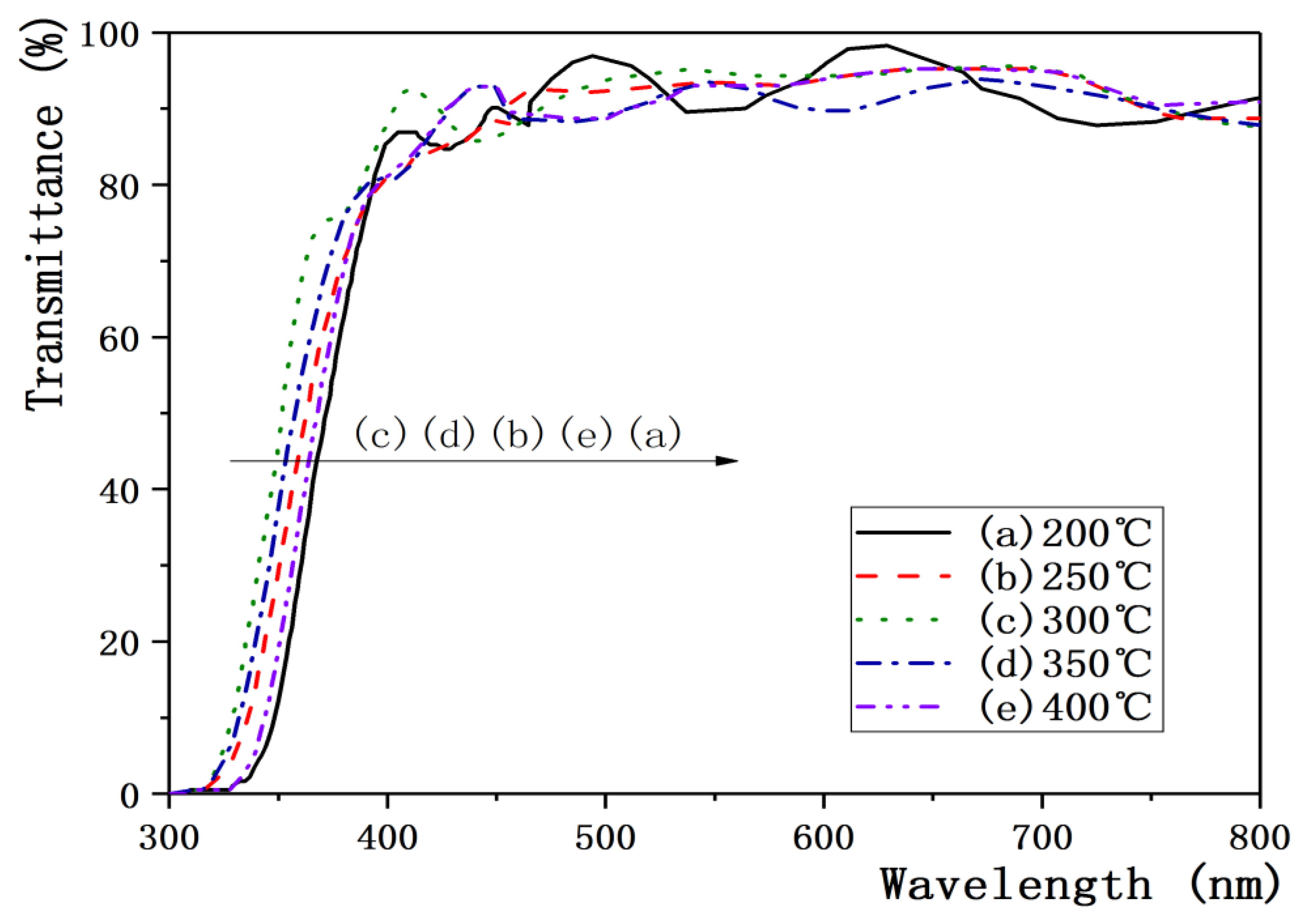
Substrates and targets are the material basis for preparing thin films by sputtering, and they are the primary factors to be considered for magnetron sputtering [82]. Substrate temperature directly affects the crystalline phase and crystal structure of the deposited films, so substrate temperature is critical for the photoelectrical properties of film [75,82]. When the substrate temperature is low, which means that the particles sputtered onto the substrate have less kinetic energy and the mobility of surface atoms is low, low-density film, rough surface, and porous amorphous structure are easily formed [75]. However, higher substrate temperature will reduce the amount of oxygen adsorbed near substrate and the particles sputtered onto substrate do not react completely due to the oxygen deficiency, resulting in many defects in the formed films [83]. Therefore, when ZnO:Ga films are produced by magnetron sputtering, the optimized substrate temperature can reduce the various defects in film and improve the film’s crystalline quality and photoelectric properties [84]. On the other hand, appropriate substrate temperature plays an important role in impure donor atoms’ movement into the lattice position [75].
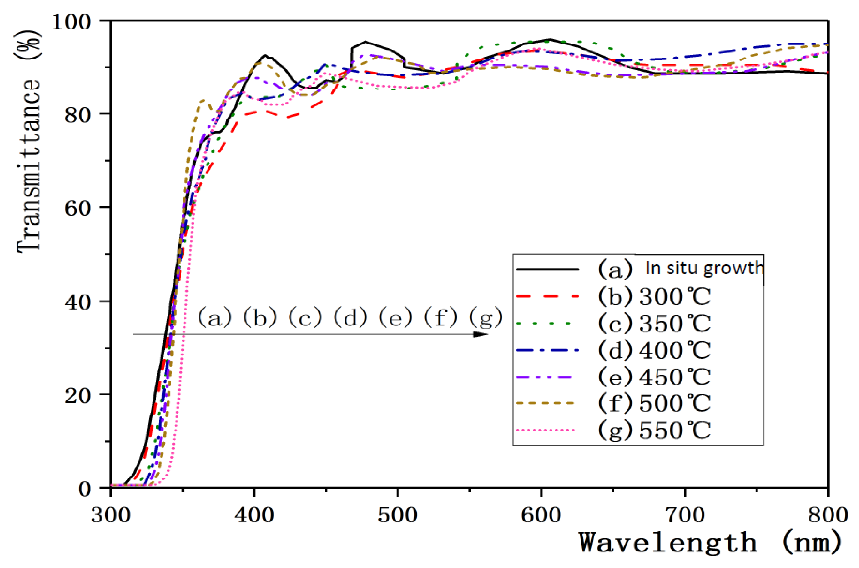
Miyaka [85] reported that the increase of substrate temperature is helpful for Zn’s replacement by Ga and the improvement of crystal quality. Higher substrate temperature helps the desorption of adsorbed oxygen in grain boundaries, which can effectively prevent the formation of Ga2O3 in the grain gap and provide more free electrons, thus the carrier concentration is improved [86]. However, as the substrate temperature continues to rise, all the electric properties begin to downgrade [87]. Chang found that more scattering centers have been formed for films deposited at higher substrate temperature [78], from which it is deduced that the ion impurity scattering is the dominant factor for the decrease of conductivity by calculating the mean free path of electrons, and that all films have high transmittance, low absorption, and a sharp fundamental cut-off absorption edge in the visible spectral range [87,88]; the transmission spectra is shown in Figure 6. Table 3 shows the lattice and performance parameters of ZnO:Ga films produced at different substrate temperature.
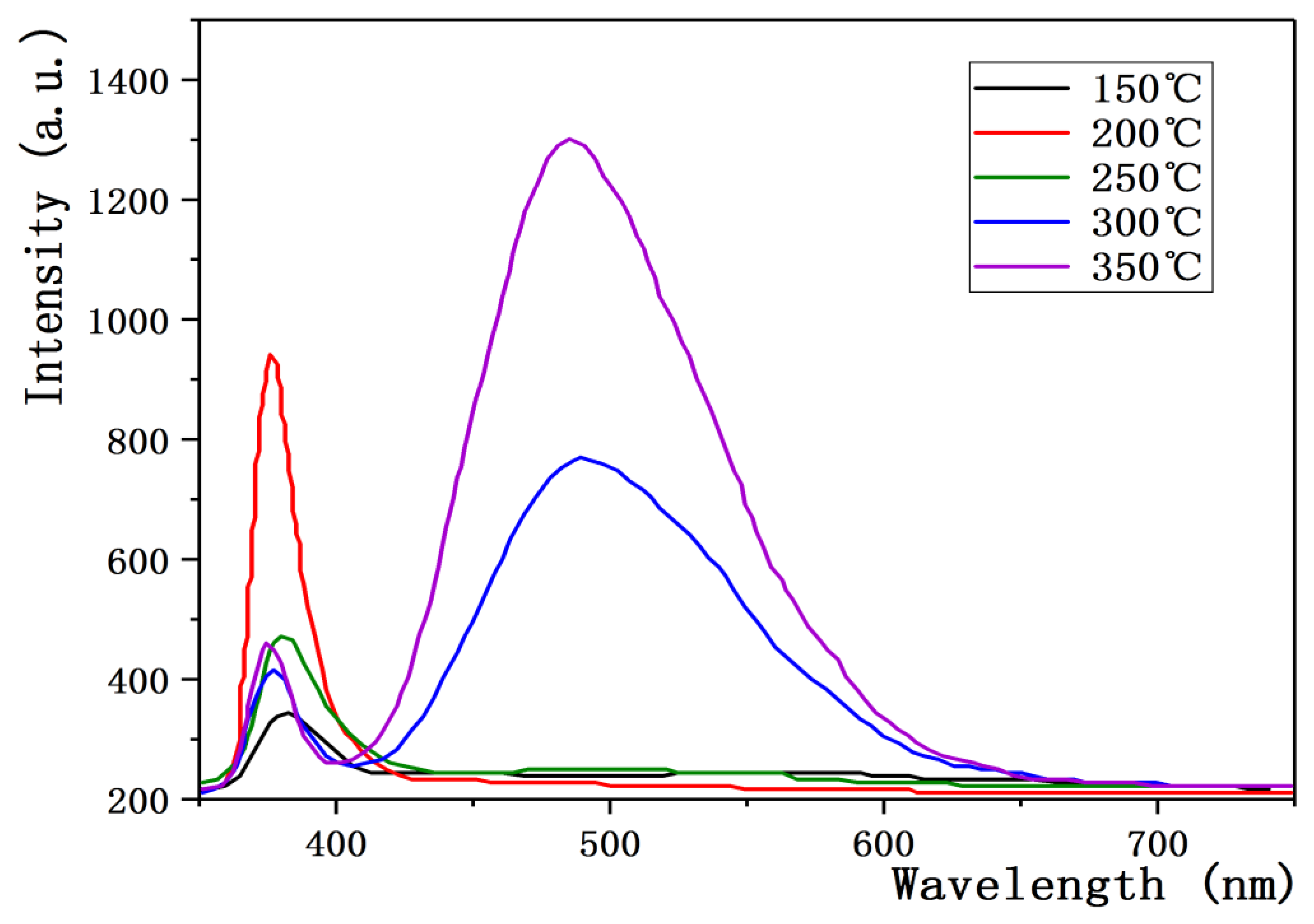
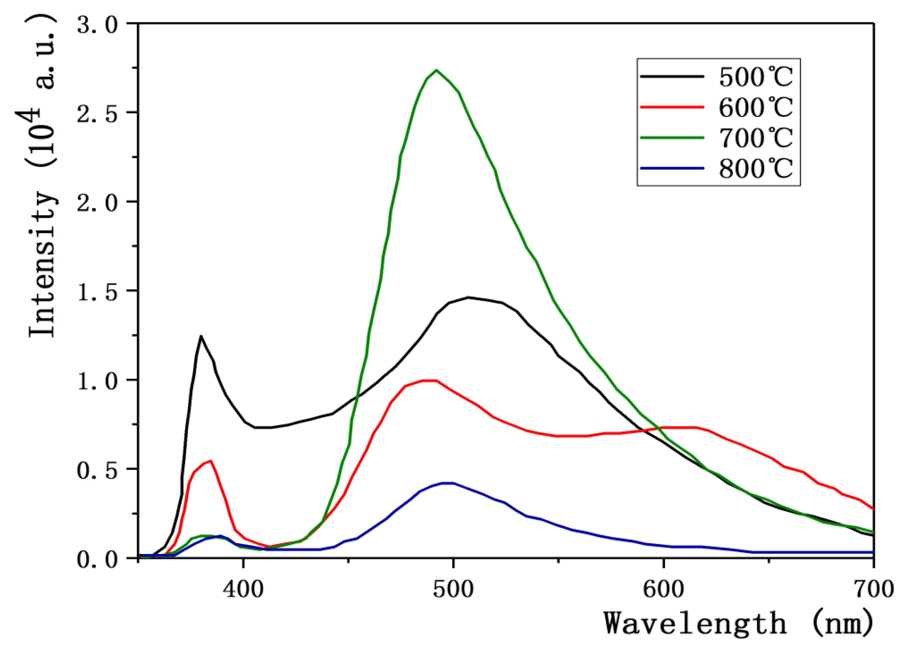
With the increase of substrate temperature, the luminescence intensity of violet and blue light components in the photoluminescence spectrum of ZnO:Ga scintillation films increase gradually. At the same time, the intensity of the green light peak also enhances a little bit [89]. In semiconductors, lattice point defects can act as very efficient traps for electrons, holes, and excitons, and strongly influence transport and optical properties of materials [90]. The residual gases Ar and O2 in the process of magnetron sputtering can cause radiation-induced chemical etching of materials. Contamination and etching effects are sensitive to temperature [91]. Therefore, the difference in ultraviolet photoluminescence spectra of ZnO films at different substrate temperatures mainly reflects the difference in lattice defect density caused by residual gases such as Ar and O2 [92]. The increase of the blue peak intensity may be attributed to the gradual increase of Zn atoms in the ZnO:Ga films. However, the explanations for the origin of the green peak have always been controversial [93]. When the substrate temperature rises, the desorbed oxygen in the films will be ejected because of high temperature, the zinc and oxygen in the films will become more disproportionate, so the density of oxygen vacancies increases remarkably, which leads to significant enhancement of the photoluminescence peak in the visible light region [94]. The photoluminescence spectrum given in Figure 7 is consistent with the above description.
3.3. Effect of Sputtering Atmosphere on Properties of ZnO:Ga Films
It was found that green peak luminescence probably corresponds to intrinsic point defects, such as oxygen vacancies, zinc vacancies, oxygen interstitial and zinc interstitial defects [96,97], so the defects have a great influence on the luminescence properties. In the process of magnetron sputtering, both oxygen’s partial pressure and annealing treatment affect the stoichiometric ratio of ZnO:Ga films, so these two factors are very important for the concentration of oxygen defects and zinc defects in the films [98]. Accordingly, the sputtering pressure is one of the important parameters for magnetron sputtering [99,100]. In the production of ZnO:Ga thin film, the gas mixture of argon and oxygen or the pure argon is commonly used [101]. Therefore, working gas pressure and fractions can be adjusted by controlling the flow rates of argon and oxygen separately [102].
If the ratio of O2 to Ar is fixed, when the sputtering pressure is low, the oxygen partial pressure is also relatively low [75,103], the mean free path of electrons in the plasma region increases, the probability that electrons collide with Ar atoms decreases, and self-sustaining discharge cannot be formed, resulting in ignition difficulty and glow discharge instability [103]. When the sputtering pressure is high, it means the probability that sputtered particles collide with the Ar particles (Ar+ and neutral Ar atoms) in plasma increases for higher oxygen partial pressure, resulting in the decrease of films’ density, adhesion, and crystallinity [104]. In general, if the working pressure increases within a reasonable range, it does not only facilitate glow, but also improves the film deposition rate to a certain extent. However, the excessive increase of working pressure may cause an increase of impurities in the cavity, which is harmful for the purity of films [75].
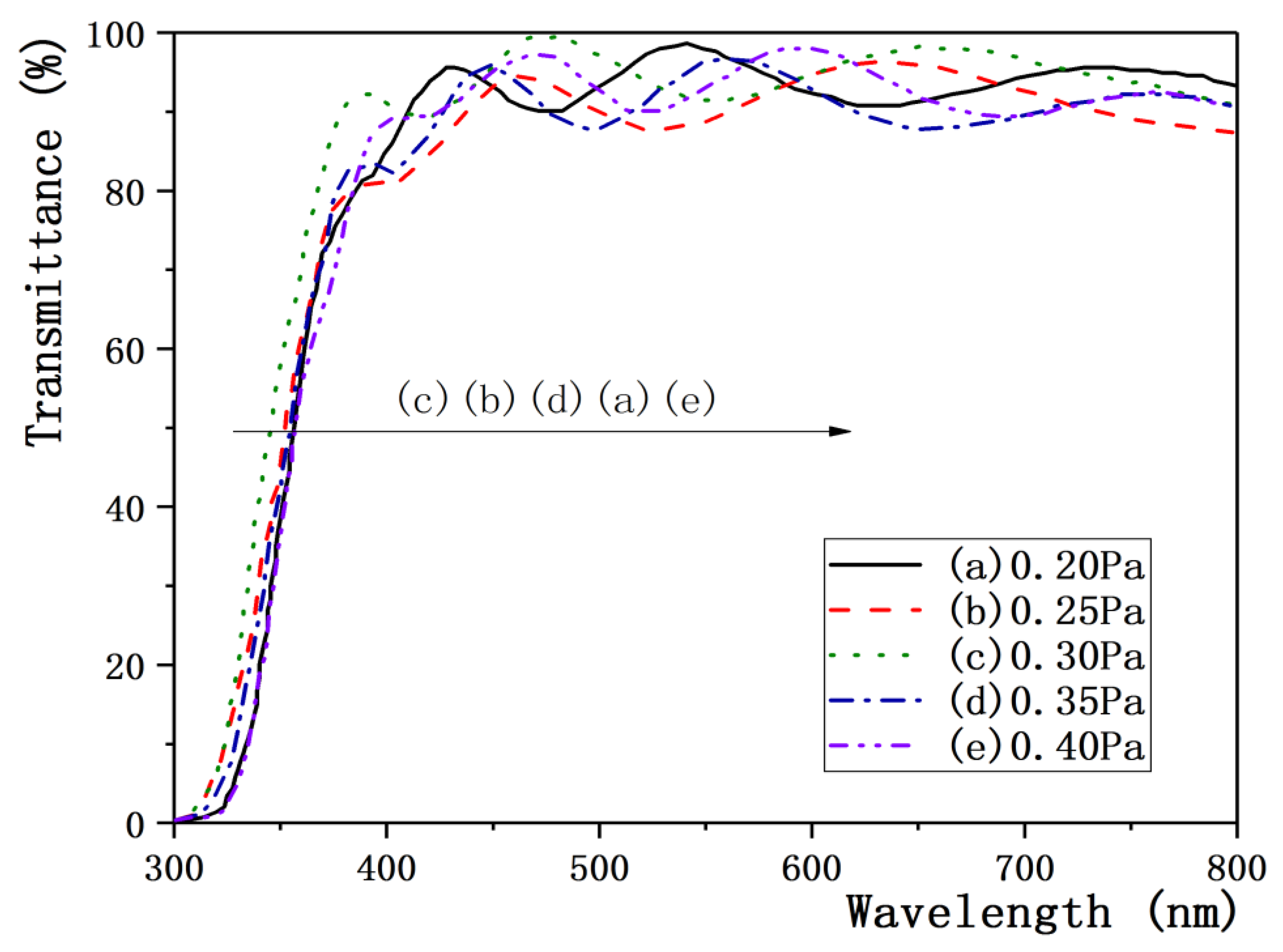
When the sputtering pressure is 1.0 Pa [75], the surface of the films is smooth, the grain stacking is compact and uniform, and there is no obvious grain boundary. When the sputtering pressure increases from 0.5 Pa to 1.0 Pa, all electric properties of the films are improved [75,100]. As the pressure continues to rise, the sputtered particles continue to be oxidized, and oxygen in the grain boundary gap is excessive, which leads to the formation of Ga2O3 and the deterioration of electrical properties [103,105]. The average transmittance is independent of the sputtering pressure, and it can reach 90% or even higher in the visible region, as shown in Figure 8 [75]. Table 4 shows the lattice parameters and performance parameters of ZnO:Ga films produced at different sputtering pressure.
If the sputtering pressure is fixed, when the oxygen partial pressure is low, the compound formed by the reaction of metal with oxygen deviates from the normal stoichiometric ratio. At this time, the doped atoms directly enter the film by sputtering, replacing the position of Zn. The less oxygen content, the more zinc is replaced by doped atoms, and the electrical and optical properties of the film are improved accordingly [106]. However, if the oxygen content is too low, there is not enough oxygen to oxidize the sputtered metal particles, which reduces the electro-optical properties of the film [63,75]. Table 5 shows the lattice parameters and performance parameters of ZnO:Ga films produced at different oxygen partial pressures, and the transmission spectra of ZnO:Ga films is shown in Figure 9.
The intensity of luminescence peak of ZnO:Ga scintillation films varies with the O2/Ar ratio, the chemical ratio of Zn to O in ZnO:Ga films depends on oxygen content, and the concentration of various intrinsic defects in the films is also affected by oxygen content [107]. Therefore, the emission spectrum of ZnO:Ga films is related to the ratio of Ar to O2 and the defects concentration. Lin [96] reported that the relationship between intrinsic defects and oxygen partial pressure in ZnO:Ga thin film can be expressed by the chemical-like reaction equation below.
where [VO×] and [VZn×] are the concentration of neutral oxygen vacancies and zinc vacancies, respectively, [Zni], [Oi], and [OZn] are, respectively, the concentration of zinc interstitial, oxygen interstitial, and oxygen dislocation. It can be seen, respectively, from Equations (8) and (9) that the VO concentration in ZnO films is inversely proportional to oxygen partial pressure PO21/2, and the VZn concentration is proportional to oxygen partial pressure PO21/2. When the O2/Ar ratio is small, the oxygen partial pressure is small, which makes the VO concentration in the films high and the VZn concentration low; when the O2/Ar ratio increases, the VO concentration decreases, while the VZn concentration increases [96].
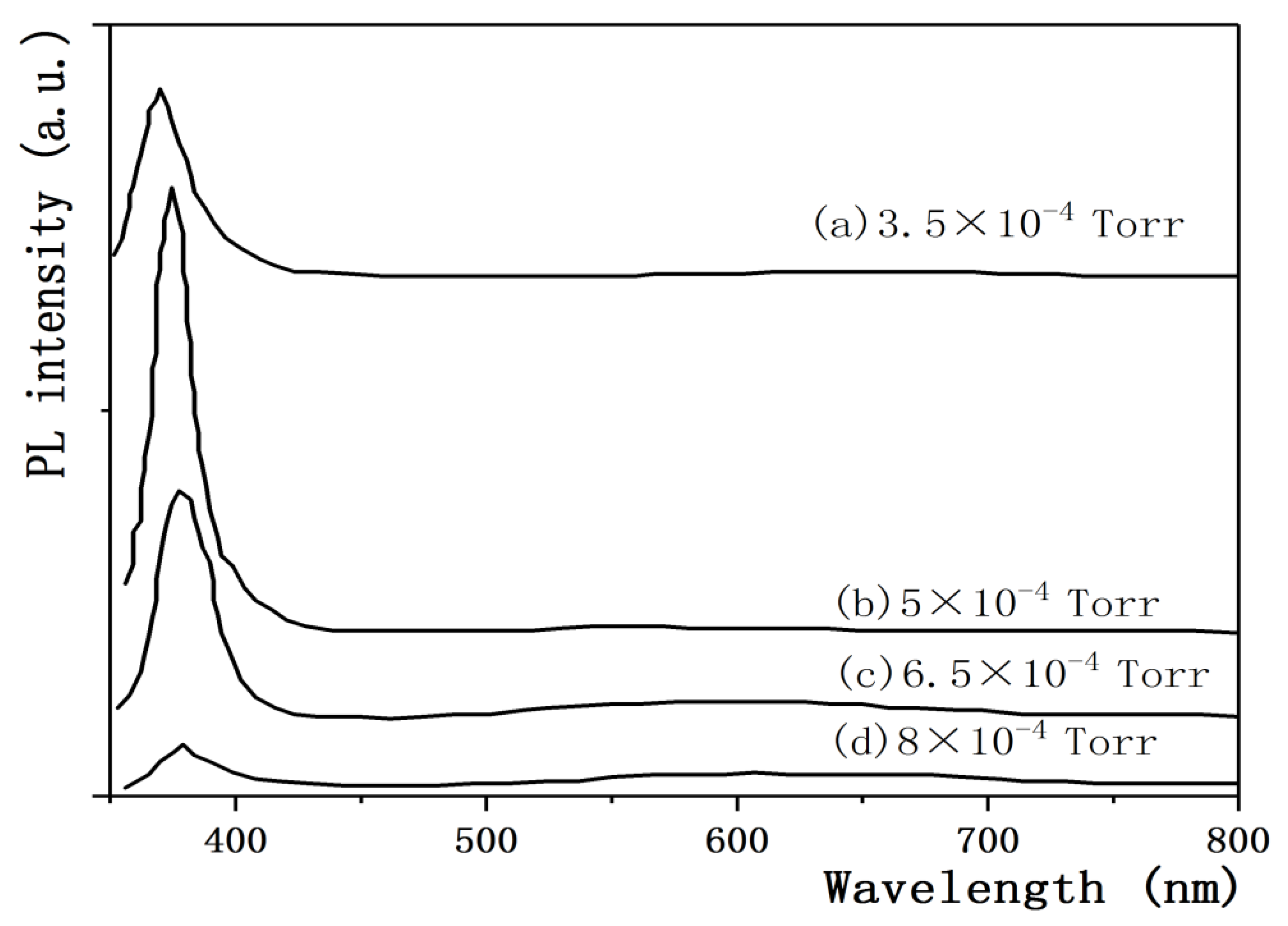
Researchers believe that the emission intensity of violet light and green light first increase and then decrease with the enhancement of oxygen partial pressure [96,108]. This is because there are a lot of defects and impurities in the films with poor crystalline quality to cause exciton quenching and a low exciton density for insufficient O2 or excessive O2 [109]. The ZnO:Ga thin films produced at a low oxygen flow rate contain more oxygen vacancy defects [108]. When the oxygen flow rate increases, the VO defects reduce and the VZn defects increase, resulting in transition inhibition between donor and acceptor, so that the green peaks of films disappear. On the other hand, the transition from the bottom of the conduction band to the acceptor level will be enhanced, resulting in a strong blue emission band [104], which is why emission intensity of the blue band in ZnO:Ga scintillation films increases. The oxygen partial pressure value of the photoluminescence spectrum given in Figure 10 is different from the above oxygen partial pressure value, but the trend in change is consistent with the above description.
3.4. Effect of Annealing Temperature on Properties of ZnO:Ga Films
The annealing treatment in the preparation process of films is an important method to reconstruct the structure, surface, and physical properties of films [111]. Its principle is to use thermal energy to eliminate defects due to the internal stress generated in the production process, which reforms the arrangement of atoms and recrystallizes the material, even becoming a single crystal with the disappearance of all defects [112]. The effects of annealing treatment on the films are as follows: (1) annealing treatment can crystallize the amorphous structure in the films [113]; (2) annealing treatment can eliminate the defects in the crystal lattice, change the surface morphology of films, and accelerate the diffusion and transfer of impurity atoms in the films; and (3) annealing treatment can release the residual stress of film materials and desorb atoms or molecules in the films, leading to improvements of the films’ properties [113].
Annealing treatment has a great influence on the crystalline quality and photoelectric and scintillation properties of the films [75,113,114]. Lower annealing temperature is helpful for the formation of micro-grains, the adjustment of film structure, and the elimination of defects in films, thus the crystal quality of the films is improved [115,116]. However, high annealing temperature will cause atoms’ polymerization in films, which will increase the size of clusters, the surface roughness and the scattering of thin films, resulting in the decrease of the crystalline quality of films [117]. The resistivity is inversely proportional to the product of mobility µ and carrier concentration n [118], and the increase of film mobility is coherent with the improvement of film crystallization quality [115]. Xing [119] found that when ZnO:Ga film is annealed in a vacuum, the concentration of Zn decreases but the concentration of O increases with the increase in annealing temperature. The increase in annealing temperature releases the residual stress in ZnO:Ga films to make the film smoother and denser, which reduces the visible light absorption and scattering [119]. However, the increase in oxygen concentration is beneficial to the formation of Ga2O3 and leads to the increase of electron traps in the films [75,119]. The transmission spectra of ZnO:Ga films is shown in Figure 11, and Table 6 shows the performance parameters of ZnO:Ga films produced at different annealing temperature.
Since the heat treatment conditions directly affect the types and concentration of defects in ZnO:Ga, the photoluminescence spectrum of ZnO:Ga films is related to the change in defects with annealing temperature [96]. Lower annealing temperature does not change the defect distribution in the films [112], but the intensity of ultraviolet emission band increases and no visible light emission can be detected [120]. When the annealing temperature increases to a higher temperature range, the blue peak shifts obviously towards the long wavelength, and the green luminescence peak begins to appear, although it is very weak compared to the strong ultraviolet emission [121]. It was considered that thin films annealed under an unstable state would cause more defects and lead to the fluctuation between UV and visible emission [122]. As the annealing temperature continues to rise, the UV emission begins to weaken and the green emission keeps increasing [121]. For higher carrier concentration, the auger effect will be produced to quench the luminescence, this is called concentration quenching [123]. The annealing temperature value of the photoluminescence spectrum given in Figure 12 is different from the above annealing temperature value, but the trend in change is consistent with the above description. Annealing is a recrystallization process in a proper temperature range, which helps to reduce defects, especially in an oxygen atmosphere. Annealing treatment helps to enhance the light radiation based on band-edge transition due to the reduction of VO defects in ZnO:Ga films and the more complete crystallization of the films [121]. As for the annealing conditions, the annealing atmosphere is also an important factor as well as temperature. The effects of annealing temperature mentioned above on ZnO:Ga films are almost always annealed in oxygen or air.
3.5. Summary
In general, sputtering parameters have a great influence on the crystalline quality and film properties. The sputtering power level means the change of deposition rate, which affects crystal structure and properties of the films [62]. Substrate temperature will lead to the change of grain size, which affects the surface morphology and properties, therefore, appropriate substrate temperature is very necessary for crystal growth [82]. The type and concentration of defects in the films are influenced by the preparation method and process conditions [124,125]. The defects of films strongly depend on the sputtering pressure, the O2/Ar ratio, and annealing temperature [98]. Besides the four sputtering parameters mentioned above, the doping concentration of Ga, the distance between target and substrate, and the composition of the target also affect the crystal quality and photoelectric and scintillation properties of ZnO:Ga thin films [75,77,126]. In fact, because the scintillation properties of ZnO:Ga thin films are strongly related to their crystalline quality [127], sputtering parameters should be optimized to reduce impurities and defects and to enhance the scintillation performance of thin films for better crystal quality of ZnO:Ga thin films.
4. The Application Research Status of ZnO:Ga in Nuclear Detection
The fluorescence decay lifetime of near-ultraviolet exciton emissions of ZnO at room temperature is only a few hundred picoseconds [8], and its strong radiation resistance makes it very attractive for the detection of high-energy particles, such as X-ray, γ-ray, and α-particle [3]. John Wilkinson [128] reported that excitonic transition in wide-gap semiconductors exhibits a sub-nanosecond radiation lifetime, especially the radiation lifetime of ZnO, which ranges from 400 ps to 900 ps. In this section, the application research status of ZnO:Ga prepared by magnetron sputtering and other production methods in nuclear radiation detection is summarized and discussed.
The sub-nanosecond decay time is difficult to precisely measure, in particular for the case of scintillation because the decay to be recorded is very fast. Typical fluorescence from commonly used organic fluorophores lasts only some hundred picoseconds to some tens of nanoseconds [129]. Time-correlated single-photon counting (TCSPC) is possible to extend the date collection over multiple cycles of excitation and emission. The method is based on the repetitive, precisely timed registration of single photons e.g., a fluorescence signal [130,131]. As a single photon sensitive detector, a photomultiplier tube (PMT), micro channel plate (MCP), single-photon avalanche diode (SPAD) or hybrid PMT can be used.
Zhang and Zheng [132] tested the fluorescence characteristics of a ZnO:Ga scintillator using a 500 fs and 248 nm ultra-short pulse ultraviolet laser system. They established a fluorescence transmission optical path to solve scattering laser interference and efficient collection of fluorescence. The fluorescence spectrum with wavelength ranging from 380 nm to 410 nm and a center wavelength of 392 nm was measured, its FWHM and rising time were 153.51 ps and 104.93 ps, respectively, which means that a femtosecond ultraviolet laser system should be used for their measurement [132]. In addition, Ma, OuYang, and Zhang et al. [133,134,135,136,137] conducted much research on the application of ZnO:Ga scintillation crystals prepared by magnetron sputtering in pulsed radiation detection, as shown in Table 7.
As mentioned above, the magnetron sputtering method is one of the most mature and widely used depositing technologies in industry [2]. However, except magnetron sputtering, other growth methods are also commonly used for the practical production and application of ZnO:Ga crystals. Koyama [138] used spark plasma sintering (SPS) to prepare 30% mol-doped ZnO:Ga phosphors at an atmospheric pressure of 8 Pa. The results show that the lifetime of a PL emission peak at 383 nm is about 20 ns, which means that ZnO:Ga phosphor material can be used as a new fluorescent material for fast neutron detectors. Cates [139] calculated the timing resolution using an analytical model and his measurements show that the achievable ZnO:Ga timing resolution is 52.5 ± 10 ps FWHM. It is believed that such a scintillator with extremely fast decay time is of great importance in many research areas that require ultrafast scintillators. In addition, Xu [140] and Zhang [141] studied the application of ZnO:Ga scintillation crystals prepared by a hydrothermal method in pulsed radiation detection, as shown in Table 8.
5. Summary
Zinc oxideis a wide band-gap semiconductor compound with broad application prospects, but the intrinsic defects and strong self-absorption effect in ZnO affect its photoelectric and scintillation properties [14,15]. At present, the research hotspots in the world are how to solve the problems of low interaction probability and low luminous efficiency when thin film scintillators detect X-rays and γ-rays [12,13], how to understand the scintillation mechanism, and how to improve the light yield of ZnO-based scintillating materials [3,17].
Adding an appropriate amount of Ga to ZnO is helpful to compensate for its intrinsic defects to a certain degree, and it also helps to reduce the loss of energy transfer and self-absorption effect, and to improve its crystallization, luminescent efficiency, and scintillation properties [5,142]. Magnetron sputtering method has many advantages: high deposition rate, high power efficiency, low substrate temperature, minor damage to the substrate, etc. [60]. However, high-energy particles can easily damage the film surface and increase the defect concentration [64]. The ZnO:Ga has an extremely fast time response, high light yield, strong irradiation resistance, and low deliquescence. Its scintillation performance can basically meet the demand for ultrafast scintillation crystals [32]. In fact, the scintillation properties of ZnO:Ga thin films are highly dependent on the crystalline quality [127], and the crystalline quality strongly depends on the sputtering parameters. Therefore, how to improve poor repeatability, how to understand the scintillation mechanism of ZnO:Ga, and how to optimize the performance of ZnO:Ga scintillation films have become bottlenecks [143]. It is hopeful that, as a new inorganic scintillation crystal, ZnO:Ga will have a very broad application prospect in nuclear radiation detection [32].
Funding
This work is supported by the “Strategic Priority Research Program” of the Chinese Academy of Sciences (Grant No. XDA10000000) and the Fundamental Research Funds for the Central Universities (Grant No. xjj2017109).
Conflicts of Interest
The authors declare no conflict of interest.
References
- Ozgur, U.; Alivov, Y.I.; Liu, C.; Teke, A.; Reshchikov, M.A.; Dogan, S.; Avrutin, V.; Cho, S.J.; Morkoc, H. A comprehensive review of ZnO materials and devices. J. Appl. Phys. 2005, 98, 041301. [Google Scholar] [CrossRef]
- Ye, Z.Z.; Lv, J.G.; Zhang, Y.Z.; He, H.P. ZnO: Doping and Application; Zhejiang University Press: Hangzhou, China, 2009. (In Chinese) [Google Scholar]
- Koike, K.; Aoki, T.; Fujimoto, R.; Sasa, S.; Yano, M.; Gonda, S.; Ishigami, R.; Kume, K. Radiation hardness of single-crystalline zinc oxide films. Phys. Status Solid(c) 2012, 9, 1577–1579. [Google Scholar] [CrossRef]
- Hausladen, P.A.; Neal, J.S.; Mihalczo, J.T. An alpha particle detector for a portable neutron generator for the Nuclear Materials Identification System (NMIS). Nucl. Instrum. Meth. Phys. Res. B 2005, 241, 835–838. [Google Scholar] [CrossRef]
- Klimm, D.; Ganschow, S.; Schulz, D.; Fornari, R. The growth of ZnO crystals from the melt. J. Cryst. Growth 2008, 310, 3009–3013. [Google Scholar] [CrossRef] [Green Version]
- Simpson, P.J.; Tjpssem, R.; Hunt, A.W.; Lynn, K.G.; Munne, V. Superfast timing performance from ZnO scintillators. Nucl. Instrum. Method Phys. Res. A 2003, 505, 82–84. [Google Scholar] [CrossRef]
- Mayo, D.C.; Nolen, J.R.; Cook, A.; Mu, R.R.; Haglund, R.F. Zinc oxide nanowire gamma ray detector with high spatiotemporal resolution. Proc. SPIE Synth. Photonics Nanoscale Mater. 2016, 9737. [Google Scholar] [CrossRef]
- Jacobsson, J.; Viarbitskaya, S.; Mukhtar, E.; Edvinsson, T. A size dependent discontinuous decay rate for the exciton emission in ZnO quantum dots. Phys. Chem. Chem. Phys. 2014, 16, 13849–13857. [Google Scholar] [CrossRef] [PubMed]
- Sinha, S.; Kwong, J.; Langeveld, W.; Ryge, P. Characterization of ZnO, BaF2 and PbWO4 scintillator detectors for cargo inspection using transmitted X-ray spectroscopy. IEEE Trans. Nucl. Sci. 2013, 60, 1016–1023. [Google Scholar] [CrossRef]
- Fujimoto, Y.; Yanagida, T.; Miyamoto, M.; Chani, V.I. Scintillation and dosimetric properties of Cu-doped zinc oxide thin films. e-J. Surf. Sci. Nanotechnol. 2014, 12, 275–278. [Google Scholar] [CrossRef]
- Melcher, C.L. Perspectives on the future development of new scintillators. Nucl. Instrum. Method Phys. Res. A 2005, 537, 6–14. [Google Scholar] [CrossRef]
- Li, Q.L.; Liu, X.L.; Hu, Y.H.; Li, F.R.; Liu, S.; Wu, Q.; Sun, Z.X.; Zhang, J.N.; Huang, S.M.; Zhang, Z.J.; et al. Development of ZnO-based nanorod arrays as scintillator layer for ultrafast and high-spatial-resolution X-ray imaging system. Opt. Express 2018, 26, 31290–31298. [Google Scholar] [CrossRef]
- Hormozan, Y.; Sychugov, I.; Linnros, J. High-resolution X-ray imaging using a structured scintillator. Med. Phys. 2016, 43, 696–701. [Google Scholar] [CrossRef] [PubMed]
- Clementi, C.; Rosi, F.; Romani, A.; Vivani, R.; Brunetti, B.G.; Miliani, C. Photoluminescence properties of zinc oxide in paints: A study of the effect of self-absorption and passivation. Appl. Spectrosc. 2012, 66, 1233–1241. [Google Scholar] [CrossRef] [PubMed]
- Ahn, C.H.; Kim, Y.Y.; Kim, D.C.; Mohanta, S.K.; Cho, H.K. A comparative analysis of deep level emission in ZnO layers deposited by various methods. J. Appl. Phys. 2009, 105, 013502. [Google Scholar] [CrossRef]
- Vempati, S.; Mitra, J.; Dawson, P. One-step synthesis of ZnO nanosheets:a blue-white fluorophore. Nanoscale Res. Lett. 2012, 7, 470. [Google Scholar] [CrossRef]
- Derenzo, S.E.; Weber, M.J.; Courchesne, E.B.; Klintenberg, M.K. The quest for the ideal inorganic scintillator. Nucl. Instrum. Method Phys. Res. A 2003, 505, 111–117. [Google Scholar] [CrossRef]
- Ye, J.; Gu, S.L.; Zhu, S.M. Fermi-level band filling and band-gap renormalization in Ga-doped ZnO. Appl. Phys. Lett. 2005, 86, 192111–192113. [Google Scholar] [CrossRef]
- Yoshioka, S.; Oba, F.; Huang, R.; Tanaka, I.; Mizoguchi, T.; Yamamoto, T. Atomic structures of supersaturated ZnO-Al2O3 solid solutions. J. Appl. Phys. 2008, 103, 140. [Google Scholar] [CrossRef]
- Sun, D.; Tan, C.L.; Tian, X.H.; Huang, Y.W. Comparative study on ZnO monolayer doped with Al, Ga and in atoms as transparent electrodes. Materials 2017, 10, 703. [Google Scholar] [CrossRef]
- Ungula, J.; Dejene, F.B.; Swart, H.C. Effects of different Ga doping concentration on structural and optical properties of Ga-doped ZnO nanoparticles by precipitation reflux method. In Proceedings of the 61st Annual Conference of the South African Institute of Physics, Johannesburg, South Africa, 4–8 July 2016. [Google Scholar]
- Ryan, M.T.; Poston, J.W. A half Century of Health Physics: 50th Anniversary of the Health Physics Society; Lippincott Williams & Wilkins: Philadelphia, PA, USA, 2005. [Google Scholar]
- Wilkinson, F. Emission Tomography: The fundamentals of PET and SPECT; Chapter 13; Elsevier: Amsterdam, The Netherlands, 2004; pp. 229–254. [Google Scholar]
- Batischev, A.G.; Aleksandrin, S.Y.; Gurov, Y.B.; Koldashov, S.V.; Lapushkin, S.V.; Mayorov, A.G. Multilayer scintillation detector for nuclear physics monitoring of space weather. Phys. Procedia 2015, 74, 132–138. [Google Scholar] [CrossRef]
- Nikl, M.; Yoshikawa, A.; Vedda, A.; Fukuda, T. Development of novel scintillator crystals. J. Cryst. Growth 2006, 292, 416–421. [Google Scholar] [CrossRef]
- Van Eijk, C.W.E. Inorganic-scintillator development. Nucl. Instrum. Method Phys. Res. A 2001, 460, 1–14. [Google Scholar] [CrossRef]
- Lehmann, W. Edge emission of n-type conducting ZnO and CdS. Solid Stat. Electron. 1966, 9, 1107–1110. [Google Scholar] [CrossRef]
- Luckey, D. A fast inorganic Scintillator. Nucl. Instrum. Method 1968, 62, 119–120. [Google Scholar] [CrossRef]
- Bourrent-Courchesne, E.D.; Derenzo, S.E.; Weber, M.J. Development of ZnO:Ga as an ultra-fast scintillator. Nucl. Instrum. Method Phys. Res. A 2009, 601, 358–363. [Google Scholar] [CrossRef] [Green Version]
- Neal, J.S.; Giles, N.C.; Yang, X.; Wall, R.A.; Ucer, K.B.; Williams, R.T.; Wisniewski, D.J.; Boatner, L.A.; Rengarajan, V.; Nause, J.; Nemeth, B. Evaluation of melt-grown, ZnO single crystals for use as alpha-particle detectors. IEEE Trans. Nucl. Sci. 2008, 55, 1397–1403. [Google Scholar] [CrossRef]
- Moses, W.W. Current trends in scintillator detectors and materials. Nucl. Instrum. Methods Phys. Res. Sect. A 2002, 487, 123–128. [Google Scholar] [CrossRef] [Green Version]
- Neal, J.S.; Boatner, L.A.; Giles, N.C.; Halliburton, L.E.; Derenzo, S.E.; Bourret-Courchesne, E.D. Comparative investigation of the performance of ZnO-based scintillators for use as α-particle detectors. Nucl. Instrum. Method Phys. Res. A 2006, 568, 803–809. [Google Scholar] [CrossRef]
- Look, D.C.; Reynolds, D.C.; Hemsky, J.W.; Jones, R.L.; Sizelove, J.R. Production and annealing of electron irradiation damage in ZnO. Appl. Phys. Lett. 1999, 75, 811–813. [Google Scholar] [CrossRef] [Green Version]
- Bergman, L.; McHale, J.L. Handbook of Luminescent Semiconductor Materials; CRC Press: Boca Raton, FL, USA, 2012. [Google Scholar]
- Bagnall, D.M.; Chen, Y.F.; Zhu, Z.; Yao, T.; Koyama, S.; Shen, M.Y.; Goto, T. Optically pumped lasing of ZnO at room temperature. Appl. Phys. Lett. 1997, 70, 2230–2232. [Google Scholar] [CrossRef]
- Khan, Z.R.; Khan, M.S.; Zulfequar, M.; Khan, M.S. Optical and structural properties of ZnO thin films fabricated by Sol-Gel method. Mater. Sci. Appl. 2011, 2, 340–345. [Google Scholar] [CrossRef]
- Hsieh, P.T.; Chen, Y.C.; Kao, K.S.; Wang, C.M. Luminescence mechanism of ZnO thin film investigated by XPS measurement. Appl. Phys. A 2008, 90, 317–321. [Google Scholar] [CrossRef]
- Manzano, C.V.; Alegre, D.; Caballero-Calero, O.; Alen, B.; Martin-Gonzalez, M.S. Synthesis and luminescence properties of electrodeposited ZnO films. J. Appl. Phys. 2011, 110, 043538. [Google Scholar] [CrossRef] [Green Version]
- Han, B.M.; Chang, S.; Kim, S.Y. Chopping effect on the crystallinity of ZnO films prepared by a r.f. planar magnetron sputtering method. Thin Solid Films 1999, 338, 265–268. [Google Scholar] [CrossRef]
- Constantin, D.G.; Apreutesei, M.; Arvinte, R.; Marin, A.; Andrei, O.C.; Munteanu, D. Magnetron sputtering technique used for coatings deposition; technologies and applications. In Proceedings of the Conference on Materials Science and Engineering-BRAMAT, Brasov, Romania, 24–26 February 2011. [Google Scholar]
- Mejia, M.I.; Restrepo, G.; Marin, J.M.; Sanjines, R.; Pulgarin, R.; Mielczarski, E.; Mielczarski, J.; Kiwi, J. Magnetron sputtered Ag surfaces. New evidence of the nature of the Ag ions intervening in bacterial inactivation. ACS Appl. Mater. Interfaces 2010, 2, 230–235. [Google Scholar] [CrossRef] [PubMed]
- Pflug, A.; Siemers, M.; Schwanke, C.; Kurnia, B.F.; Sittinger, V.; Szyszka, B. Simulation of plasma potential and ion energies in magnetron sputtering. Mater. Technol. 2011, 26, 10–14. [Google Scholar] [CrossRef]
- Wang, J.; Wei, W.; Zhang, B.; Liu, W.; Tang, K.; Fan, L.; Pei, X.; Hong, Y.; Xu, Y.; Wang, Y.S. Simulation of the trajectory of electrons in a magnetron sputtering system of TIN with CST particle studio. In Proceedings of the Conference: IPAC14, Dresden, Germany, 15–20 June 2014; pp. 2341–2343. [Google Scholar]
- Aijaz, A. Design and Characterization of a Synchronous Co-Axial Double Magnetron Sputtering System; Linkoping University: Linkoping, Sweden, 2009. [Google Scholar]
- Jilani, A.; Abdel-wahab, M.S.; Hammad, A.H. Advance deposition techniques for thin film and coating. In Modern Technologies for Creating the Thin-Film Systems and Coatings; InTech: London, UK, 2017. [Google Scholar] [CrossRef]
- Alami, J.; Sarakinos, K.; Mark, G.; Wutting, M. On the deposition rate in a high power pulsed magnetron sputtering discharge. Appl. Phys. Lett. 2006, 89, 154104. [Google Scholar] [CrossRef] [Green Version]
- Anders, A.; Andersson, J.; Ehiasarian, A. High power impulse magnetron sputtering: Current-voltage-time characteristics indicate the onset of sustained self-sputtering. J. Appl. Phys. 2007, 102, 113303. [Google Scholar] [CrossRef] [Green Version]
- Mattox, D.M. Handbook of Physical Vapor Deposition(PVD) Processing: Film Formation, Adhesion, Surface Preparation and Contamination Control. Available online: https://www.sciencedirect.com/book/9780815514220/handbook-of-physical-vapor-deposition-pvd-processing (accessed on 20 April 2019).
- Guttler, D. An Investigation of Target Poisoning during Reactive Magnetron Sputtering; Technichen Universitat Dresden: Saxony, Germany, 2008. [Google Scholar]
- Silva-Bermudez, P.; Ramirez, G.; Rodil, S.E. Corrosion Resistant Coatings for Dental Implants. Bio-Tribocorrosion in Biomaterials and Medical Implants; Woodhead Publishing: Sawston, Cambridge, UK, 2013; pp. 250–308. [Google Scholar]
- Feist, C.; Plankensteiner, A.; Winkler, J. Studying target erosion in planar sputtering magnetrons using a discrete model for energetic electrons. In Proceedings of the Conference: COMSOL 2013, Rotterdam, The Netherlands, 23–25 October 2013. [Google Scholar]
- Nakano, T. Study of Particle Transport in High Pressure Sputter Deposition Process; Seikei University: Musashino, Japan, 2001. [Google Scholar]
- Vaha-Nissi, M.; Hirvikorpi, T.; Mustonen, T.; Karppinen, M.; Harlin, A. Thin film deposition techniques—Steps towards more sustainable packages. In Proceedings of the 2010 TAPPI International Conference on Nanotechnology for the Forest Product Industry, Espoo, Finland, 27–29 September 2010. [Google Scholar]
- Douglass, D. Thin-Film Coatings: Thin-Film Manufacturing Considerations for Semiconductor Lasers; Laser Focus World: Nashua, NH, USA, 2018. [Google Scholar]
- Ohshima, E.; Ogino, H.; Niikura, I.; Maeda, K.; Sato, M.; Ito, M.; Fukuda, T. Growth of the 2-in-size bulk ZnO single crystals by the hydrothermal method. J. Cryst. Growth 2004, 260, 166–170. [Google Scholar] [CrossRef]
- Sekiguchi, T.; Miyashita, S.; Obara, K.; Shishido, T. Hydrothermal growth of ZnO single crystal and their optical characterization. J. Cryst. Growth 2000, 214, 72–76. [Google Scholar] [CrossRef]
- Kim, H.; Horwitz, J.S.; Pique, A.; Gilmore, C. Electrical and optical properties of indium tin oxide thin films grown by pulsed laser deposition. Appl. Phys. A 1999, 69, 447–450. [Google Scholar] [CrossRef]
- Gabas, M.; Diaz-Carrasco, P.; Agullo-Rueda, F.; Fernandez, P.H. High quality ZnO and Ga:ZnO thin films grown onto crystalline Si(1 0 0)by RF magnetron sputtering. Sol. Energy Mater. Sol. Cells 2011, 95, 2327–2334. [Google Scholar] [CrossRef]
- Yao, H.C.; Chiu, M.C.; Wu, W.T.; Shieu, F.S. Influence of radio frequency bias on the characteristics of TiO2 thin films prepared by DC sputtering. J. Electrochem. Soc. 2006, 153, 237–243. [Google Scholar] [CrossRef]
- Thorsen, A.C.; Manasevit, H.M. Heteroepitaxial GaAs on aluminum oxide: Electrical properties of undoped films. J. Appl. Phys. 1971, 42, 2519. [Google Scholar] [CrossRef]
- Wasa, K.; Kitabatake, M.; Adachi, H. Thin Film Materials Technology: Sputtering of Compound Materials; Willian Andrew Publishing: Norwich, UK, 2004. [Google Scholar]
- Chan, K.Y.; Teo, B.S. Sputtering power and deposition pressure effects on the electrical and structural properties of copper thin films. J. Mater. Sci. 2005, 40, 5971–5981. [Google Scholar] [CrossRef]
- Wang, W.W.; Diao, X.G.; Wang, Z.; Yang, M.L. Preparation and characterization of high-performance direct current magnetron sputtered ZnO:Al films. Thin Solid Films 2005, 491, 54–60. [Google Scholar] [CrossRef]
- Ma, Q.B.; Ye, Z.S.; He, H.P.; Wang, J.R. Preparation and characterization of transparent conductive ZnO:Ga films by DC reactive magnetron sputtering. Mater. Charact. 2008, 59, 124–128. [Google Scholar] [CrossRef]
- Drude, P. Zur Elektronentheorie der Metalle. Annalen der physik 1900, 306, 566–613. [Google Scholar] [CrossRef] [Green Version]
- Drude, P. Zur Elektronentheorie der Metalle:II.Teil.Galvanomagnetische und thermomagnetische Effecte. Annalen der physik 1900, 308, 369–402. [Google Scholar] [CrossRef]
- Purcell, E.M.; Morin, D.J. Electricity and Magnatism; McGraw-Hill: New York, NY, USA, 1965; pp. 117–122. [Google Scholar]
- Frank, G.; Kauer, E.; Kostlin, H. Transparent heat-reflecting coatings based on highly doped semiconductors. Thin Solid Films 1981, 77, 107–118. [Google Scholar] [CrossRef]
- Wu, W.F.; Chiou, B.S. Deposition of indium tin oxide films on polycarbonate substrate by radio-frequency magnetron sputtering. Thin Solid Films 1997, 298, 221–227. [Google Scholar] [CrossRef]
- Qiao, Z.H.; Agashe, C.; Mergel, D. Dielectric modeling of transmittance spectra of thin ZnO:Al films. Thin Solid Films 2006, 496, 520–525. [Google Scholar] [CrossRef]
- Fujiwara, H.; Kondo, M. Effects of carrier concentration on the dielectric function of ZnO:Ga and In2O3:Sn studied by spectroscopic ellipsometry: Analysis of free-carrier and band-edge absorption. Phys. Rev. B 2005, 71, 075109. [Google Scholar] [CrossRef]
- Sernelius, B.E.; Berggren, K.F.; Jin, Z.C.; Hamberg, I.I.; Grangvist, C.G. Band-gap tailoring of ZnO by means of heavy Al doping. Phys. Rev. B 1988, 37, 10244. [Google Scholar] [CrossRef]
- Jin, Z.C.; Hamberg, I.; Granqvist, C.G. Optical properties of sputter-deposited ZnO:Al thin films. J. Appl. Phys. 1988, 64, 5117. [Google Scholar] [CrossRef]
- Peter, K.; Willeke, G.; Prasad, K.; Shah, A. Free-carrier absorption in microcrystalline silicon thin films prepared by very-high frequency glow discharge. Philos. Mag. B 1994, 69, 197. [Google Scholar] [CrossRef]
- Ma, Q.B. Preparation and Characterization of Transparent High Conductivity Near Infrared Reflective ZnO:Ga Thin Films; Zhejiang University: Hangzhou, China, 2007. (In Chinese) [Google Scholar]
- Cullity, B.D. Elements of X-ray Diffraction, 2nd ed.; Addison Wesley: Reading, MA, USA, 1978. [Google Scholar]
- Gomez, H.; Maldonado, A.; Olvera, M.L.; Acosta, D. Gallium-doped ZnO thin films deposited by chemical spray. Acosta Sol. Energy Mater. Sol. Cells 2005, 87, 107–116. [Google Scholar] [CrossRef]
- Chang, J.F.; Hon, M.H. The effect of deposition temperature on the properties of Al-doped zinc oxide thin films. Thin Solid Films 2001, 386, 79–86. [Google Scholar] [CrossRef]
- Salameh, B.; Alsmadi, A.M.; Akkad, F.E. Physicochemistry of point defects in fluorine doped zinc tin oxide thin films. Thin Solid Films 2017, 626, 76–84. [Google Scholar] [CrossRef]
- Tauc, J. Optical properties and electronic structure of amorphous Ge and Si. Mater. Res. Bull. 1968, 3, 37–46. [Google Scholar] [CrossRef]
- Amala, R.A.; Ernest, S. Structural, morphological, optical and compositional characterization of spray deposited Ga doped ZnO thin film for Dye-Sensitized Solar Cell application. Super Micro 2014, 75, 398–408. [Google Scholar] [CrossRef]
- Huang, P.C.; Huang, C.H.; Lin, M.Y.; Chou, C.Y. The effect of sputtering parameters on the film properties of molybdenum back contact for CIGS solar cells. Int. J. Photoenergy 2013, 2013. [Google Scholar] [CrossRef]
- Jacobs, C.B.; Maksov, A.B.; Muckley, E.S.; Collins, L. UV-activated ZnO films on a flexible substrate for room temperature O2 and H2O sensing. Sci. Rep. 2017, 7, 6053. [Google Scholar] [CrossRef] [PubMed]
- Lee, S.H.; Cheon, D.H.; Kim, W.J.; Ham, M.H. Ga-doped ZnO films deposited with varying sputtering powers and substrate temperatures by pulsed DC magnetron sputtering and their property improvement potentials. Appl. Surf. Sci. 2012, 258, 6537–6544. [Google Scholar] [CrossRef]
- Miyake, A.; Yamada, T.; Makino, H. Structural, electrical and optical properties of Ga-doped ZnO films on cyclo-olefin polymer substrates. Thin Solid Films 2009, 517, 3130–3133. [Google Scholar] [CrossRef]
- Fu, E.G.; Zhuang, D.M.; Zhang, G.; Yang, W.F.; Zhao, M. Substrate temperature dependence of the properties of ZAO thin films deposited by magnetron sputtering. Appl. Surf. Sci. 2003, 217, 88–94. [Google Scholar] [CrossRef]
- Kim, K.H.; Park, K.C.; Ma, D.Y. Structural, electrical and optical properties of aluminum doped zinc oxide films prepared by radio frequency magnetron sputtering. J. Appl. Phys. 1997, 81, 7764. [Google Scholar] [CrossRef]
- Hong, R.J.; Jiang, X.; Szyszka, B.; Sittinger, V.; Pflug, A. Studies on ZnO:Al thin films deposited by in-line reactive mid-frequency magnetron sputtering. Appl. Surf. Sci. 2003, 207, 341–350. [Google Scholar] [CrossRef]
- Xu, X.L.; Ma, S.Y.; Chen, Y.; Zhang, G.H. Structure and luminescence properties of ZnO films prepared by RF magnetron sputtering. Spectrosc. Spectr. Anal. 2008, 28, 2028–2032. [Google Scholar]
- Tongay, S.; Suh, J.; Ataca, C.; Fan, W. Defects activated photoluminescence in two-dimensional semiconductors: Interplay between bound, charged, and free excitons. Sci. Rep. 2013, 3, 2657. [Google Scholar] [CrossRef]
- Myhajlenko, S. Luminescence of Solids; Springer Science+Business Media: New York, NY, USA, 1988. [Google Scholar]
- Carozo, V.; Wang, Y.X.; Fujisawa, K.; Carvalho, B.R. Optical identification of sulfur vacancies: Bound excitons at the edges of monolayer tungsten disulfide. Sci. Adv. 2017, 3, 1602813. [Google Scholar] [CrossRef]
- Ramamoorthy, K.; Sanjeeviraja, C.; Jayachandran, M.; Sankaranarayanan, K.; Misra, P.; Kukreja, L.M. Development of a novel high optical quality ZnO thin films by PLD for III–V opto-electronic devices. Curr. Appl. Phys. 2006, 6, 103–108. [Google Scholar] [CrossRef]
- Vanheusden, K.; Warren, W.L.; Seager, C.H.; Tallant, D.R. Mechanisms behind green photoluminescence in ZnO phosphor powders. J. Appl. Phys. 1996, 79, 7983. [Google Scholar] [CrossRef]
- Saha, D.; Das, A.K.; Ajimsha, R.S.; Misra, P. Effect of disorder on carrier transport in ZnO thin films grown by atomic layer deposition at different temperatures. J. Appl. Phys. 2013, 114, 043703. [Google Scholar] [CrossRef]
- Lin, B.X.; Fu, Z.X.; Jia, Y.B. Green luminescent center in undoped zinc oxide films deposited on silicon substrates. Appl. Phys. Lett. 2001, 79, 943. [Google Scholar] [CrossRef]
- Fabbri, F.; Vilani, M.; Catellani, A.; Calzolari, A. Zn vacancy induced green luminescence on non-polar surfaces in ZnO nanostructures. Sci. Rep. 2014, 4, 5158. [Google Scholar] [CrossRef] [PubMed] [Green Version]
- Yuste, M.; Galindo, R.E.; Caretti, I.; Torres, R. Influence of the oxygen partial pressure and post-deposition annealing on the structure and optical properties of ZnO films grown by dc magnetron sputtering at room temperature. J. Phys. D: Appl. Phys. 2012, 45, 025303. [Google Scholar] [CrossRef]
- Igasaki, Y.; Kanma, H. Argon gas pressure dependence of the properties of transparent conducting ZnO:Al films deposited on glass substrates. Appl. Surf. Sci. 2001, 169–170, 508–511. [Google Scholar] [CrossRef]
- Assunção, V.; Fortunato, E.; Marques, A.; Aguas, H. Influence of the deposition pressure on the properties of transparent and conductive ZnO:Ga thin-film produced by r.f. sputtering at room temperature. Thin Solid Films 2003, 427, 401–405. [Google Scholar] [CrossRef]
- Sam, Z. Organic Nanostructured Thin Film Devices and Coatings for Clean Energy; CRC Press: Boca Raton, FL, USA, 2010. [Google Scholar]
- Fairose, S.; Ernest, S.; Daniel, S. Effect of oxygen sputter pressure on the structural, morphological and optical properties of ZnO thin films for gas sensing application. Sens. Imaging 2018, 19, 1. [Google Scholar] [CrossRef]
- Ma, Q.B.; Zhu, L.P.; Ye, Z.S.; He, H.P.; Wang, J.R.; Hu, S.H.; Zhao, B.H. Influence of sputtering pressure on the properties of ZnO:Ga films prepared by DC reactive magnetron sputtering. China J. Semicond. 2007, 28, 285–288. (In Chinese) [Google Scholar]
- Song, D.Y.; Aberle, A.G.; Xia, J. Optimisation of ZnO:Al films by change of sputter gas pressure for solar cell application. Appl. Surf. Sci. 2002, 195, 291–296. [Google Scholar] [CrossRef]
- Castro, M.V.; Tavares, C.J. Dependence of Ga-doped ZnO thin film properties on different sputtering process parameters: Substrate temperature, sputtering pressure and bias voltage. Thin Solid Films 2015, 586, 13–21. [Google Scholar] [CrossRef] [Green Version]
- Gies, A.; Pecquenard, B.; Benayad, A.; Martinez, H. Effect of total gas and oxygen partial pressure during deposition on the properties of sputtered V2O5 thin films. Solid State Ion. 2005, 176, 1627–1634. [Google Scholar] [CrossRef]
- Hussain, S.; Khan, Y.; Khranovskyy, V.; Muhammad, R. Effect of oxygen content on the structural and optical properties of ZnO films grown by atmospheric pressure MOCVD. Proc. Natl. Sci. Mater. Int. USA 2013, 23, 44–50. [Google Scholar] [CrossRef] [Green Version]
- Ahn, C.H.; Kim, Y.Y.; Kang, S.W.; Kong, B.H. Dependency of oxygen partial pressure on the characteristics of ZnO films grown by radio frequency magnetron sputtering. J. Mater. Sci. Mater. Electron. 2008, 19, 744–748. [Google Scholar] [CrossRef]
- Xu, X.L.; Lau, S.P.; Chen, J.S.; Chen, G.Y. Polycrystalline ZnO thin films on Si(1 0 0) deposited by filtered cathodic vacuum arc. J. Cryst. Growth 2001, 223, 201–205. [Google Scholar] [CrossRef]
- Wang, Y.G.; Lau, S.P.; Lee, H.W.; Yu, S.F. Comprehensive study of ZnO films prepared by filtered cathodic vacuum arc at room temperature. J. Appl. Phys. 2003, 94, 1597. [Google Scholar] [CrossRef]
- Wang, Y.; Lee, S.; Vilmercati, P.; Lee, H.N. Atomically flat reconstructed rutile TiO2(0 0 1) surfaces for oxide film growth. Appl. Phys. Lett. 2016, 108, 091604. [Google Scholar] [CrossRef]
- Xu, J.P.; Shi, S.B.; Li, L.; Song, Z.X. Effects of annealing temperature on structural and optical properties of ZnO thin films. Chin. Phys. Lett. 2010, 27, 047803. [Google Scholar]
- Ahn, B.D.; Oh, S.H.; Lee, C.H.; Kim, G.H. Influence of thermal annealing ambient on Ga-doped ZnO thin films. J. Cryst. Growth 2007, 309, 128–133. [Google Scholar] [CrossRef]
- Hsieh, P.T.; Chen, Y.C.; Kao, K.S.; Wang, C.M. Structural and luminescent characteristics of non-stoichiometric ZnO films by various sputtering and annealing temperatures. Phys. B 2008, 403, 178–183. [Google Scholar] [CrossRef]
- Ma, Q.B.; Ye, Z.Z.; He, H.P.; Zhu, L.P. Influence of annealing temperature on the properties of transparent conductive and near-infrared reflective ZnO:Ga films. Scr. Mater. 2008, 58, 21–24. [Google Scholar] [CrossRef]
- Heo, S.B.; Jeon, J.H.; Gong, T.K.; Moon, H.J. Influence of a Ni interlayer on the optical and electrical properties of trilayer GZO/Ni/GZO films. Ceram. Int. 2015, 48, 157–163. [Google Scholar] [CrossRef]
- Mahdhi, H.; Ayadi, Z.B.; Gauffier, J.L.; Djessas, K. Influence of sputtering power on the properties of thin layers of GZO for photovoltaic applications. J. Mater. Sci. Mater. Electron. 2015, 26, 3336–3343. [Google Scholar] [CrossRef]
- Gotz, W.; Kern, R.S.; Chen, C.H.; Liu, H. Hall-effect characterization of III—V nitride semiconductors for high efficiency light emitting diodes. Mater. Sci. Eng. B 1999, 59, 211–217. [Google Scholar] [CrossRef]
- Xing, G.Z.; Yao, B.; Cong, C.X.; Yang, T. Effect of annealing on conductivity behavior of undoped zinc oxide prepared by RF magnetron sputtering. J. Alloys Compd. 2008, 457, 36–41. [Google Scholar] [CrossRef]
- Hsieh, P.T.; Chen, Y.C.; Wang, C.M.; Tsai, Y.Z. Structural and photoluminescence characteristics of ZnO films by room temperature sputtering and rapid thermal annealing process. Appl. Phys. A 2006, 84, 345–349. [Google Scholar] [CrossRef]
- Ungula, J.; Dejene, B.F.; Swart, H.C. Effect of annealing on the structural, morphological and optical properties of Ga-doped ZnO nanoparticles by reflux precipitation method. Results Phys. 2017, 7, 2022. [Google Scholar] [CrossRef]
- Wang, Y.G.; Lau, S.P.; Lee, H.W.; Yu, S.F. Photoluminescence study of ZnO films prepared by thermal oxidation of Zn metallic films in air. J. Appl. Phys. 2003, 94, 354–358. [Google Scholar] [CrossRef]
- Hiller, D.; Lopez-Vidrier, J.; Gutsch, S.; Zacharias, M. Defect-induced luminescence quenching vs. charge carrier generation of phosphorus incorporated in silicon nanocrystals as function of size. Sci. Rep. 2017, 7, 863. [Google Scholar] [CrossRef]
- Zhang, Y.T.; Du, G.T.; Liu, D.L.; Wang, X.Q. Crystal growth of undoped ZnO films on Si substrates under different sputtering conditions. J. Cryst. Growth 2002, 243, 439–443. [Google Scholar] [CrossRef]
- Kohan, A.F.; Ceder, G.; Morgan, D. First-principles study of native point defects in ZnO. Phys. Rev. B 2000, 61, 15019–15027. [Google Scholar] [CrossRef]
- Ma, Q.B.; Ye, Z.Z.; He, H.P.; Hu, S.H. Structural, electrical, and optical properties of transparent conductive ZnO:Ga films prepared by DC reactive magnetron sputtering. J. Cryst. Growth 2007, 304, 64–68. [Google Scholar] [CrossRef]
- Negi, S.; Rana, M.P.S.; Gautam, S.K.; Singh, R.G. Structural and optical modification of Ga-doped zinc oxide thin films induced by thermal annealing. Indian J. Pure Appl. Phys. 2016, 54, 236–240. [Google Scholar]
- John, W.; Ucer, K.B.; Williams, R.T. Picosecond excitonic luminescence in ZnO and other wide-gap semiconductors. Radiat. Meas. 2004, 38, 501–505. [Google Scholar]
- Wahl, M. Time-Correlated Single Photon Counting. Available online: https://www.picoquant.com/images/uploads/page/files/7253/technote_tcspc.pdf (accessed on 20 April 2019).
- Lakowicz, J.R. Principles of Fluorescence Spectroscopy, 3rd ed.; Springer Science+Business Media: New York, NY, USA, 2006. [Google Scholar]
- Conner, O.D.V.O.; Phillips, D. Time-Correlated Single Photon Counting; Academic Press: London, UK, 1984. [Google Scholar]
- Zhang, Y.S.; Zheng, G.X. 500 fs UV laser system and its application to fluorescence test of thin film scintillators. Opt. Precis. Eng. 2011, 19, 475–481. (In Chinese) [Google Scholar] [CrossRef]
- Ma, Y.L.; Ouyang, X.P.; Zhang, J.W.; Zhang, Z.B. Properties study of ZnO:Ga crystal on pulsed radiation detections. Chin. Phys. C 2010, 34, 354–358. [Google Scholar]
- Ma, Y.L.; Ouyang, X.P.; Zhang, Z.B.; Zhang, J.W. Response of ZnO:Ga crystal to proton beam. Atomic Energy Sci&Tech 2009, 43, 848–850. (In Chinese) [Google Scholar]
- Ma, Y.L.; Ouyang, X.P.; Chen, L.; Zhang, Z.B.; Zhang, J.W.; Quan, L.; Luo, J.H.; Zhou, H.S.; Guo, Y.J. Time and energy response of ZnO:Ga crystal to hard X-ray. High Power Laser Part. Beams 2008, 20, 2088–2090. (In Chinese) [Google Scholar]
- Ma, Y.L.; Ouyang, X.P.; Zhang, Z.B.; Zhang, J.W. Study on Response of ZnO:Ga Crystal to Single Heavy Charged Particle. Atom. Energy Sci. Technol. 2009, 43, 170–173. (In Chinese) [Google Scholar]
- Zhang, Q.M.; Yan, J.; Deng, B.J.; Zhang, J.W.; Lv, J.G.; Wen, X.; Gao, K.Q. An ultrafast X-ray scintillating detector made of ZnO(Ga). J. Instrum. 2017, 12, 12033. [Google Scholar] [CrossRef]
- Koyama, S.; Nanto, H.; Kinoshita, A.; Fujiwara, A. Neutron scintillator using Ga-doped ZnO phosphor with high detection efficiency. In Proceedings of the 2008 IEEE Nuclear Science Symposium Conference, Dresden, Germany, 19–25 October 2008. [Google Scholar]
- Cates, J.W.; Hayward, J.P.; Zhang, X. Measurement of achievable timing resolution with ZnO:Ga films. IEEE Trans. Nucl. Sci. 2013, 60, 3127–3133. [Google Scholar] [CrossRef]
- Xu, M.X.; Chen, L.; Yao, Z.M.; Ren, S.Q. Transient radiation imaging based on a ZnO:Ga single-crystal image converter. Sci. Rep. 2018, 8, 4178. [Google Scholar] [CrossRef]
- Zhang, Y.Q.; Wang, J.L.; Ren, M.D. Study of Hydrothermal Growth Process and Properties of ZnO:Ga Crystal. Superhard Mater. Eng. 2016, 28, 57–62. (In Chinese) [Google Scholar]
- Cheong, K.Y.; Muti, N.; Ramanan, S.R. Electrical and optical studies of ZnO:Ga thin films fabricated via the sol-gel technique. Thin Solid Films 2002, 410, 142–146. [Google Scholar] [CrossRef]
- Shin, S.W.; Sim, K.U.; Moon, J.H.; Kim, J.H. The effect of processing parameters on properties of Ga-doped ZnO thin films by RF magnetron sputtering. Curr. Appl. Phys. 2010, 11, 274–277. [Google Scholar] [CrossRef]
Figure 1.
The energy levels diagram of lattice defects in intrinsic ZnO semiconductors [16].
Figure 1.
The energy levels diagram of lattice defects in intrinsic ZnO semiconductors [16].

Figure 2.
The photoluminescence spectrum of ZnO thin films at room temperature [36].
Figure 2.
The photoluminescence spectrum of ZnO thin films at room temperature [36].

Figure 3.
Schematic diagram of the magnetron sputtering principle [41].
Figure 3.
Schematic diagram of the magnetron sputtering principle [41].


Figure 5.
Transmission spectra of ZnO:Ga films prepared at different sputtering power [75].
Figure 5.
Transmission spectra of ZnO:Ga films prepared at different sputtering power [75].

Figure 6.
Transmission spectra of ZnO:Ga films prepared at different substrate temperature [75].
Figure 6.
Transmission spectra of ZnO:Ga films prepared at different substrate temperature [75].

Figure 7.
The photoluminescence spectra of ZnO thin films grown at different substrate temperatures [95].
Figure 7.
The photoluminescence spectra of ZnO thin films grown at different substrate temperatures [95].

Figure 8.
Transmission spectra of ZnO:Ga films prepared at different sputtering pressures [75].
Figure 8.
Transmission spectra of ZnO:Ga films prepared at different sputtering pressures [75].

Figure 9.
Transmission spectra of ZnO:Ga films prepared at different oxygen partial pressures [75].
Figure 9.
Transmission spectra of ZnO:Ga films prepared at different oxygen partial pressures [75].

Figure 10.
The photoluminescence spectra of ZnO thin films grown at different oxygen partial pressures [110].
Figure 10.
The photoluminescence spectra of ZnO thin films grown at different oxygen partial pressures [110].

Figure 11.
Transmission spectra of ZnO:Ga films prepared at different annealing temperatures [75].
Figure 11.
Transmission spectra of ZnO:Ga films prepared at different annealing temperatures [75].

Figure 12.
The photoluminescence spectra of ZnO thin films grown at different annealing temperatures [112].
Figure 12.
The photoluminescence spectra of ZnO thin films grown at different annealing temperatures [112].


| Depositing Methods | Vacuum Thermal Evaporation | Ion Plating Evaporation | Magnetron Sputtering | Chemical Vapor Deposition | Sol-Gel Method | Atomic Layer Deposition |
|---|---|---|---|---|---|---|
| Materials | metals or low melting point materials | metals and dielectrics | metals and dielectrics | dielectric materials | materials with melting point above 500 °C | metals, dielectrics and polymer |
| Uniformity | poor | excellent | good | excellent | good | very good |
| Grain Size (nm) | 10–100 | 10–100 | –10 | 1–100 | 0.5–500 | <1 nm |
| Deposition Rate (nm/s) | 1.67–1167 | 1.67–833.5 | 0.167–8.335 | 1–10 | very slow | 0.1 |
| Deposition Quality | poor | excellent | good | excellent | poor | good |
| Porosity | high | no porosity, but many defects | lower, but more gaseous impurities | lower | higher | low |
| Substrate Temperature (°C) | 50–100 | 50–200 | –200 | 150–2000 | 300–800 | 50–500 |
| Adhesion | poor | excellent | good | good | good | good |
Table 2.
The performances of ZnO:Ga films produced at different sputtering power [75].
Table 2.
The performances of ZnO:Ga films produced at different sputtering power [75].
| Sputtering Power(W) | 100 | 120 | 140 | 160 | 180 |
|---|---|---|---|---|---|
| FWHM (°) | 0.41 | 0.37 | 0.35 | 0.42 | 0.47 |
| Grain size (nm) | 23.9 | 26.4 | 27.4 | 22.9 | 20 |
| Resistivity (× 10−4Ω·cm) | 8.0 | 4.52 | 3.0 | 4.42 | 6.8 |
| Mobility (cm2/V·s) | 6.82 | 7.85 | 8.32 | 6.77 | 5.98 |
| Carrier concentration (× 1021cm−3) | 1.16 | 1.78 | 2.53 | 2.12 | 1.56 |
| Optical band-gap (eV) | 3.595 | 3.65 | 3.76 | 3.71 | 3.62 |
Table 3.
The performances of ZnO:Ga films produced at different substrate temperature [75].
Table 3.
The performances of ZnO:Ga films produced at different substrate temperature [75].
| Substrate Temperature (°C) | 200 | 250 | 300 | 350 | 400 |
|---|---|---|---|---|---|
| FWHM (°) | 0.43 | 0.38 | 0.36 | 0.37 | 0.426 |
| Grain size (nm) | 22.6 | 25.5 | 27.0 | 26.1 | 22.8 |
| Resistivity (× 10−4Ω·cm) | 13.0 | 6.34 | 3.0 | 4.0 | 8.1 |
| Mobility (cm2/V·s) | 3.8 | 5.48 | 8.32 | 6.95 | 4.38 |
| Carrier concentration (× 1021/cm3) | 1.28 | 1.82 | 2.5 | 2.22 | 1.78 |
Table 4.
The performances of ZnO:Ga films produced at different sputtering pressures [75].
Table 4.
The performances of ZnO:Ga films produced at different sputtering pressures [75].
| Sputtering Pressure (Pa) | 0.5 | 0.7 | 1.0 | 1.5 | 2.0 | 2.5 |
|---|---|---|---|---|---|---|
| FWHM (°) | 0.415 | 0.393 | 0.35 | 0.363 | 0.374 | 0.418 |
| Grain size (nm) | 23.4 | 24.7 | 27.4 | 26.7 | 25.9 | 23.2 |
| Resistivity (× 10−4Ω·cm) | 16.33 | 9.08 | 3.0 | 4.17 | 8.1 | 23.45 |
| Mobility (cm2/V·s) | 4.55 | 4.7 | 8.31 | 8.02 | 7.4 | 4.18 |
| Carrier concentration (× 1021 cm−3) | 0.85 | 1.46 | 2.5 | 1.875 | 1.06 | 0.28 |
Table 5.
The performances of ZnO:Ga films produced at different oxygen partial pressures [75].
Table 5.
The performances of ZnO:Ga films produced at different oxygen partial pressures [75].
| Oxygen Partial Pressure (Pa) | 0.2 | 0.25 | 0.3 | 0.35 | 0.4 |
|---|---|---|---|---|---|
| FWHM (°) | 0.485 | 0.362 | 0.35 | 0.371 | 0.49 |
| Grain size (nm) | 17.23 | 22.32 | 27.42 | 22.45 | 17.03 |
| Resistivity (× 10−4Ω·cm) | 9.45 | 6.46 | 3.01 | 8.33 | 12.14 |
| Mobility (cm2/V·s) | 5.01 | 6.12 | 8.33 | 5.57 | 4.85 |
| Carrier concentration (× 1021 cm−3) | 1.32 | 1.59 | 2.5 | 1.36 | 1.06 |
Table 6.
The performances of ZnO:Ga films produced at different annealing temperatures [75].
Table 6.
The performances of ZnO:Ga films produced at different annealing temperatures [75].
| Annealing Temperature (°C) | 300 | 350 | 400 | 450 | 500 | 550 |
|---|---|---|---|---|---|---|
| Resistivity (× 10-4Ω·cm) | 2.94 | 2.88 | 2.85 | 2.6 | 2.8 | 4.39 |
| Mobility (cm2/V·s) | 8.98 | 9.73 | 10.56 | 11.83 | 13.28 | 14.77 |
| Carrier concentration (× 1021 cm−3) | 2.41 | 2.28 | 2.13 | 2.09 | 1.74 | 1.0 |
| Optical band-gap (eV) | 3.74 | 3.74 | 3.726 | 3.72 | 3.66 | 3.59 |
Table 7.
The application of ZnO:Ga scintillation crystals prepared by magnetron sputtering in radiation detection.
Table 7.
The application of ZnO:Ga scintillation crystals prepared by magnetron sputtering in radiation detection.
| Crystal Size | Measurement | Performances | Application | |
|---|---|---|---|---|
| 1. [133] | diameter: 50 mm thickness: 50 µm | time response to femtosecond laser | rise time: 104.9 ps FWHM: 153.5 ps decay time: 0.097 nm | fast time response in femtosecond level detection |
| 2. [134] | thickness: 300 µm | pulsed proton | well reflected intensity characteristics of pulsed proton source | as a recoil proton detector to detect pulsed neutron |
| 3. [135] | diameter: 50 mm thickness: 50 µm | the time response and energy response to the pulsed hard X-ray | FWHM: 440 ps rise time: 315 ps energy response above 40 KeV was very flat | a new type of hard X-ray energy spectrum measuring material |
| 4. [136] | Φ50 µm × 50 µm | time response to single α-particle | rise time: 342 ps FWHM: 686 ps | the monitoring of α-particles |
| 5. [137] | thickness: ~ µm | X-ray | fluorescence lifetime: 173 ps, FWHM: 355.1 ps light yield: 14,740 photons/MeV | Ultra-fast X-ray scintillating detector |
Table 8.
The application of ZnO:Ga scintillation crystals prepared by a hydrothermal method in radiation detection.
Table 8.
The application of ZnO:Ga scintillation crystals prepared by a hydrothermal method in radiation detection.
| Reference [140] | Reference [141] | |
|---|---|---|
| Crystal size | Φ40 mm × 1 mm | 32.36 mm × 27.46 mm × 5.52 mm |
| Measurement | the spatial distribution of cathode electron emission in intense current diode | crystal growth rate and crystal quality |
| Performances | 63.94 arcsec FWHM, fast response speed, 5.5% Bi4E3O12 (BGO) luminescence intensity, 8% luminous non-uniformity | excellent crystalline quality, 11arcsec FWHM of +c[002] crystal plane, the transmittance began to decrease at 750 nm, |
| Application | high time resolution diagnosis of pulsed radiation field | in the visible and infrared regions at wavelength greater than 750 nm |
© 2019 by the authors. Licensee MDPI, Basel, Switzerland. This article is an open access article distributed under the terms and conditions of the Creative Commons Attribution (CC BY) license (http://creativecommons.org/licenses/by/4.0/).
Share and Cite
MDPI and ACS Style
Wen, X.; Zhang, Q.; Shao, Z. Magnetron Sputtering for ZnO:Ga Scintillation Film Production and Its Application Research Status in Nuclear Detection. Crystals 2019, 9, 263. https://doi.org/10.3390/cryst9050263
AMA Style
Wen X, Zhang Q, Shao Z. Magnetron Sputtering for ZnO:Ga Scintillation Film Production and Its Application Research Status in Nuclear Detection. Crystals. 2019; 9(5):263. https://doi.org/10.3390/cryst9050263
Chicago/Turabian StyleWen, Xin, Qingmin Zhang, and Zhuang Shao. 2019. "Magnetron Sputtering for ZnO:Ga Scintillation Film Production and Its Application Research Status in Nuclear Detection" Crystals 9, no. 5: 263. https://doi.org/10.3390/cryst9050263
Note that from the first issue of 2016, this journal uses article numbers instead of page numbers. See further details here.