Growth of Metal Halide Perovskite, from Nanocrystal to Micron-Scale Crystal: A Review


1
Low Dimensional Quantum Physics & Device Group, State Key Discipline Laboratory of Wide Band Gap Semiconductor Technology, School of Microelectronics, Xidian University, 2 South Taibai Road, Xi’an 710071, China
2
Department of Nanochemistry, Istituto Italiano di Tecnologia, via Morego 30, 16163 Genova, Italy
3
Graduate School of Life Science and Systems Engineering, Kyushu Institute of Technology, 2-4 Hibikino, Wakamatsu-ku, Kitakyushu 808-0196, Japan
*
Authors to whom correspondence should be addressed.
Crystals 2018, 8(5), 182; https://doi.org/10.3390/cryst8050182
Submission received: 27 March 2018
/
Revised: 17 April 2018
/
Accepted: 17 April 2018
/
Published: 24 April 2018
(This article belongs to the Special Issue Metal Halide Perovskite Crystals: Growth Techniques, Properties and Emerging Applications)
Abstract
:Metal halide perovskite both in the form of nanocrystal and thin films recently emerged as the most promising semiconductor material covering a huge range of potential applications from display technologies to photovoltaics. Colloidal inorganic and organic–inorganic hybrid metal halide perovskite nanocrystals (NCs) have received tremendous attention due to their high photoluminescence quantum yields, while large grain perovskite films possess fewer defects, and a long diffusion length providing high-power conversion efficiency in planar devices. In this review, we summarize the different synthesis routes of metal halide perovskite nanocrystals and the recent methodologies to fabricate high-quality micron scale crystals in the form of films for planar photovoltaics. For the colloidal synthesis of halide perovskite NCs, two methods including ligand-assisted reprecipitation and hot injection are mainly applied, and the doping of metal ions in NCs as well as anion exchange reactions are widely used to tune their optical properties. In addition, recent growth methods and underlying mechanism for high-quality micron size crystals are also investigated, which are summarized as solution-process methods (including the anti-solvent method, solvent vapor annealing technology, Ostwald ripening, additive engineering and geometrically-confined lateral crystal growth) and the physical method (vapor-assisted crystal growth).
1. Introduction
Metal halide perovskite is emerging as a promising semiconductor and efficient light-harvester in high-performance, low-cost and large-coverage photovoltaics [1,2,3]. The high optical coefficient makes it a good candidate as the thin absorber layer, and the long diffusion length of both electrons and holes leads to high short-circuit current density. On the one hand, halide perovskite nanocrystals (NCs) are used for photovoltaics, which have received tremendous attention due to their high photoluminescence quantum yields, reaching almost 100%. Moreover, nanocrystals have the advantage of optical tunability compared to their bulk. On the other hand, for planar perovskite devices, a verity of preparation methods for micron-scale crystals have been promoted including the one-step methylammonium lead iodide (MAPbI3) solution, two-step sequence spin-coating and vapor-coevaporation. However, the quality of the crystals and devices are not as good as one would expect as these methods usually leads to polynanocrystal films. Although these methods lead to more than 20% power-conversion efficiency in photovoltaics, recent studies have shown that impurities and defects lead to high carrier recombination, limiting further device performance. In addition, the small size of crystal grains results in obvious hysteresis phenomena, and also leads to a diffusion length of around 1 µm, which is not comparable with single crystals with a typical diffusion length of 100 µm [4,5,6]. In terms of environmentally friendly devices and materials, due to the containment of the toxic element lead in the metal halide perovskite, thin films are preferred in the real applications. Furthermore, because of the rapid degradation of light absorption with the decrease in thickness, the quality of grown perovskite crystals needs to be improved. Recent advances in the technique and methods have made it possible to grow high-quality metal halide perovskite cyrstals both at nano-scale and micron-scale. In this review, we focus on the synthesis of halide perovskite nanocrystals and their post-synthesis transformations as well as recent technology to fabricate high-quality large crystal films for planar photovoltaics.
2. The Fabrication of Lead Halide Perovskite Colloidal Nanocrystals
Lead halide perovskites (LHP) in the form of colloidal nanocrystals (NCs), such as organic–inorganic CH3NH3PbX3, (MAPbX3), CH(NH2)2PbX3 (FAPbX3) and all-inorganic CsPbX3 LHPs (X = Cl, Br, I) have been intensively investigated for various applications including light-emitting devices (LEDs) and photodetectors, due to their color-tunable and narrow-band emissions as well as easy synthesis, convenient solution-based processing, and low fabrication cost [7,8,9,10,11,12,13]. Various approaches have been proposed for the direct synthesis of metal and organometal halide perovskite colloidal NCs (e.g., CsPbX3, MAPbX3, FAPbX3, X− = Cl−, Br−, I−), among which the most common are the hot-injection and the ligand-assisted reprecipitation (LARP) approaches.
2.1. Colloidal Synthesis of MAPbX3 Nanocrystals (NCs)
Motivated by the rapid development of the lead halide perovskite (LHP) thin films as a light-harvesting material for solar-cell applications, first colloidal synthesis of MAPbBr3 NCs was carried out by the Pérez-Prieto et al. by sthe olvent-induced reprecipitation approach [15]. Nanocrystals were stabilized by using octylammonium bromide and octadecylammonium bromide as surfactants and were colloidally stable for up to 3 months. The absorption and photoluminescence (PL) peaks of these highly crystalline of MAPbBr3 NCs were at 527 and 530 nm, respectively with a photoluminescence quantum yield (PLQY) of ~20%. Later, Zhang et al. modified the aforementioned procedure and introduced the LARP approach for the synthesis of MAPbX3 NCs by replacing octylammonium bromide and octadecylammonium bromide with n-octylamine and oleic acid as a co-ligands system into the reprecipitation process [14]. As shown in Figure 1, this method is based on the reprecipitation of lead halide (PbX2, X = Cl, Br, I) and organic halide (CH3NH3X, X = Cl, Br, I) salts in the presence of ligands; for instance, lead halide and organic halide salts are dissolved in strongly polar solvents like dimethylformamide (DMF) and are subsequently added dropwise to a solution of a non-polar medium like toluene in the presence of ligands. The miscibility gap between polar and non-polar solvents solubility consequently triggers the recrystallization of lead halide perovskite NCs. The NCs obtained were brightly luminescent with absolute PLQYs up to 70% in the case of CH3NH3PbBr3 quantum dots (QDs), for which the transmission electron microscope (TEM) image and X-ray diffraction (XRD) results are shown in Figure 2a,b. The ligands’ role was further investigated and it was observed that in absence of the octylamine, precursors undergo fast crystallization that leads to larger NCs with very low PLQY and subsequently precipitated out of the solution.
The same approach was further extended to synthesize CH3NH3PbX3 QDs (X = Cl, I) through halide substitutions. Interestingly, they successfully demonstrated a series of colloidal CH3NH3PbX3 QDs with tunable compositions by simply adjusting the ratios of PbX2 salts in the precursor solution, see Figure 2c shows that the PL spectra can be finely tuned from 407 to 734 nm by varying the halide composition (X = Br, Cl, and I).
Later, hot injection-based synthesis of MAPbX3 (X = Br, I) was reported by Vybornyi et al. [16] As shown in Figure 1, this alternative synthesis route is basically an ionic metathesis approach that does not involve any polar solvent. Methylamine solution in THF was injected into a solution of PbX2 (X = Br, I) in Octadecene (ODE)-containing long-chain capping ligands (an octylamine (OAm)/oleic acid (OA) mixture). The proton needed to form CH3NH3+ is provided by OA whereas PbX2 serves as both the Pb2+ and X− source, releasing Pb-oleate as a byproduct. MAPbBr3 NPLs, NWs and nearly cubic shape MAPbI3 NCs were successfully obtained by varying the amounts of surfactants (OAm/OA). Resultant NCs have poor optical properties compared to the NCs synthesized by LARP. Basically, the main limitation of the LARP method and two-precursor hot-injection method (precursor 1: Cs-oleate, precursor 2: Lead halide salt complex) is that both methods employ PbX2 (X = Cl, Br, or I) salts as both lead and halide precursors. Therefore, in both of these cases, one is not allowed to precisely tune the amount of reaction species. In order to overcome the restrictions associated with the aforementioned synthetic procedures, recently Imran et al. introduced a new colloidal synthesis approach that can lead to either all-inorganic or organic–inorganic lead-based halide perovskite NCs [17]. The synthesis relies on the use of acyl halides as halide precursors that can be easily injected, at any temperature, into a solution of metal cations to trigger the nucleation and the growth of the halide NCs. Acyl halides, commonly used as versatile building blocks in organic chemistry reactions, are well known for their strong reactivity toward nucleophilic compounds (e.g., amines, alcohols, carboxylic acids) to form carboxylic acid derivatives (e.g., amides, esters, anhydrides) and releasing at the same time halide anions [18]. By simply adjusting the relative amount of cation precursors, ligands, solvents, benzoyl halides and the injection temperature, it was possible to synthesize either all-inorganic or organic-inorganic APbX3 (A = Cs, MA or FA and X = Cl, Br or I) NCs with excellent control over the size distribution, very high phase purity and excellent optical properties [17]. MAPbX3 NCs synthesized by this method have nearly cubic morphology and very high phase purity in all cases (see Figure 2d–i). Resultant NCs were characterized with narrow emission line width from 15 nm to 43 nm along with very high PLQY up to 92% in case of MAPbBr3 (see Figure 2j–l).
2.2. Colloidal Synthesis of CsPbX3 NCs
The formerly reported LARP strategy was further extended by Sun et al. for the preparation of fully inorganic LHP NCs [19]. The synthesis of CsPbX3 (X− = Cl−, Br−, I−) spherical quantum dots was performed at room temperature (i.e., 25 °C) by mixing a solution of precursors in good solvent (such as N,N-dimethylformamide, DMF; tetrahydrofuran, THF; and dimethyl sulfoxide, DMSO) into a poor solvent (such as toluene and hexane). The shape control of CsPbX3 NCs was also demonstrated such as nanocubes, one-dimensional nanorods, and two-dimensional nanoplatelets a few unit cells in thickness by choosing different organic acid and amine ligands (see Figure 3a,b). Another liquid phase method is to trigger the nucleation and growth of platelets at room temperature (RT) by the injection of acetone in a mixture of precursors [20].
Protesescu et al. first developed a polar solvent-free two step ionic metathesis approach for the colloidal synthesis of brightly luminescent CsPbX3 NCs [21]. As shown in Figure 1, typically the CsPbX3 NCs were obtained by reacting the Cs-oleate with lead halide in boiling ODE solvent at 140–200 °C in the presence of a binary ligand system composed of aliphatic carboxylic acids and primary amines as surfactants to stabilize the NCs. Owing to the ionic nature of the ternary compound, very fast nucleation and growth kinectics of the NCs (1–3 s) were witnessed by in situ PL measurement with a charged coupled device (CCD) array detector, and the overall reaction mechanism can be summarized in the following equation:
These CsPbX3 NCs possess bright luminescence with narrow emission-line width typically from 11–42 nm. The PL peak position can be engineered across the entire visible spectrum by simply adjusting the halide composition (Cl:Br or Br:I) or by altering the size of the NCs. Later, a three precursor-based modified hot-injection method was developed by the Manna group which overcame the limitation of using lead halide salts as a source of both lead and halide ions. Very briefly, CsPbX3 NCs were synthesized by dissolving metal cations (cesium carbonate and lead acetate) in octadecene by using oleylamine and oleic acid as a surfactants. Subsequently, the solution was heated up to the desired temperature (170–200 °C) and the benzoyl halide precursor was swiftly injected into the reaction flask, triggering the immediate nucleation and growth of the NCs. This simple synthesis method results in very monodisperse, strongly fluorescent NCs with high-phase purity and with narrow emission linewidth along with PLQY as high as 92% (see Figure 3c–k) [17]. In general, cesium lead halide-based perovskite NCs exhibit excellent optical properties, while CsPbCl3 NCs are typically characterized by a significant non-radiative decay [22,23]. Interestingly, CsPbCl3 NCs were of particular interest from the recently developed synthesis protocol by Manna group where they reported PLQY for CsPbCl3 NCs as high as 65%, which is a record value, as shown in Figure 3c,f,i [17]. It is worth mentioning that such a high PLQY was observed only when employing a large excess of the Cl precursor, i.e., 1.8 mmol of benzoyl chloride and 0.2 mmol of the Pb precursor while with weak PL emission when the same NCs were prepared using a lower amount of benzoyl chloride [17].
The recent studies on the crystal structure of halide perovskite show that in small NCs, the reduced sizes result in broad Bragg peaks, causing the structure analysis to be more difficult than the bulk analysis. Recently, a consensus has been reached that the average structure of CsPbBr3 NCs is assigned to be the orthorhombic phase at RT [24,25]. More recently, Bertolotti et al. used advanced atomistic modeling of synchrotron wide-angle X-ray total scattering data to demonstrate that orthorhombic subdomains form which are hinged through a 2D or 3D network of twin boundaries into a pseudocubic phase [26]. By contrast with the previous reports, the as-synthesized highly luminescent in red CsPbI3 NCs, which were considered to be ideally cubic [21], were also found to have the same structure as the well-known orthorhombic CsPbBr3 phase [26]. Structural analysis for most of the lead halide perovskite nanocrystals reported in the literature was carried out by the XRD technique which is probably the most convenient option but not precise enough to conclude the formation of different phases. For instance, the cubic phase was initially reported for CsPbBr3 NCs in a majority of the reports but later it turns out to be orthorhombic by in depth investigation. Therefore, particular attention is required for the structural analysis and, most importantly, the use of reliable technique such as synchrotron which is sensitive enough to give precise information about different phases.
In the CsPbX3 NCs family, CsPbI3 with a band gap of 1.73–1.80 eV is the most interesting one for photovoltaics application but it suffers from undesired phase transition from the 3D phase (perovskite) to the 1D (non-perovskite) yellow phase of CsPbI3. Several strategies have been proposed to overcome the instability of the 3D (perovskite) phase of CsPbI3 both in films and solution. Protesecu et al. proposed that the 3D phase of CsPbI3 NCs can be stabilized by incorporating large organic cation (10% of FA+) [27] while Liu et al. recently demonstrated the increased stability of CsPbI3 NCs by introducing trioctylphosphine (TOP) as a surfactant [28]. A later method of preparation of TOP-PbI2 precursor takes at least one week, while the same approach does not work for other lead halide counterparts that limits its potential [28]. Akkerman et al. also reported the increase in the stability of CsPbI3 perovskite phase over up to a month by replacing Pb2+ with Mn2+ without altering the optical properties of the host material [29]. Imran et al. introduced benzoyl halide as an efficient halide precursor for the synthesis of lead halide perovskite NCs which allows them to work under halide excess conditions. They observed that synthesized CsPbI3 NCs were stable in both films and colloidal solution for several weeks under ambient conditions. The improved stability of 3D-phase CsPbI3 NCs was ascribed to the formation of lead halide terminated surfaces, in which Cs cations were partially replaced by alkylammonium ions [17]. Lead halide perovskite NCs with this type of surface have been reported to have improved stability and enhanced optical properties. Apart from the stability issues of CsPbI3 NCs, the quantum-confined blue emitting CsPbBr3 nano platelets/nanosheets with thickness of a few unit cells aggregate and turn green when dry solid films were prepared [12,30]. This shifting of emission band to the bulk band gap of CsPbBr3 is preventing several potential applications including blue light-emitting diodes (LEDs).
As the most used procedure for CsPbX3 NCs synthesis, the hot-injection method is a very promising methodology to achieve high-quality perovskite NCs. Xianghong He et al. [31] reviewed the effect of various parameters (ligand, reaction temperature) in the solution-fabrication strategies of all-inorganic trihalide perovskite NCs. In this approach, OA and OLA can break the cubic symmetry and lead to anisotropic growth of CsPbBr3. Shorter chain carboxylic acids give rise to larger size nanocubes from a high-temperature reaction, while shorter chain amines result in thinner nanoplatelets [32]. The Manna group has successfully synthesized the lead-based perovskite NCs with different morphology by adjusting the ligands [12,33]. Adjusting the ratio of short (octanoic acid (OA) and octylamine (OAm)) to long (OA and OAm) ligands leads to 2–3 unit cell thick CsPbBr3 nanosheets with lateral size from 300 nm up to 5 μm [12]. While adjusting the ratio of Amine with hex acid leads to CsPbBr3 nanowires with widths from 5.1 nm to 2.8 nm at a reaction temperature of 65 °C [33].
Reaction temperature also plays a role in the shape and the size of the resultant NCs. The Kovalenko group [21] showed that the size of CsPbX3 NCs is tuned in the range of 4–15 nm by varying the reaction temperature (140–200 °C). The CsPbX3 NCs were changed from nanocubes to nanoplates at lower temperatures (between 90 °C and 130 °C) [34].
2.3. Colloidal Synthesis of FAPbX3 NCs
Although the synthesis of CsPbX3 and MAPbX3 NCs has been optimized over the last few years, FAPbX3 NCs with optimal optical properties as well as a narrow size distribution and phase purity have not yet been prepared by either hot-injection techniques or by the LARP approach. Recently, FAPbX3 in the form of NCs have received considerable interest due to several potential advantages over their cesium and methylammonium counterparts, for instance higher stability due to a more symmetrical and tightly packed crystal structure, and impressive optical properties [35,36,37].
Protesescu et al. reported a polar solvent-free three-step hot-injection method for the synthesis of FAPbX3 (X = Br, I) NCs. In a typical hot-injection synthesis, FA-Pb precursor solution was prepared by reacting Pb and FA acetates with oleic acid in octadecene. Subsequently, temperature was increased to 130 °C and oleylammonium bromide dissolved in toluene was rapidly injected. The NCs obtained have nearly cubic morphology and very high PLQY up to 85%. But its potential versatility was limited by the poor reactivity of the alkylammonium halide salts that leads to the formation of undesired secondary phases and the resultant NC contains 10% of phase impurity (NH4Pb2Br5) [27,39]. Later on Levchuk et al. reported colloidal synthesis of FAPbX3 (X = Cl, Br, I, or mixed Cl/Br and Br/I) NCs of 15−25 nm sizes by LARP, see Figure 4a–c [38]. The emission wavelength can be tuned from 415−740 nm by tailoring halide composition as well as by their thickness with narrow full width at half-maximum (FWHM) of 20−44 nm (see Figure 4d). Resulting NCs are characterized by radiative lifetimes of 5−166 ns and very high PLQY (up to 85%) but the shape control was poor in all the cases [38,40]. To overcome the limitation imposed by traditional synthesis methods, the Manna group recently reported a modified three-precursor hot-injection method for the synthesis of FAPbX3 NCs by using benzoyl halide as a halide precursor. Interestingly, this approach allows one to work with the desired stoichiometry of the ions, since the halide ions and the metal cation sources are not delivered together, i.e., they are not delivered with the same chemical precursor. In a typical synthesis, formamidinium acetate and lead acetate were dissolved and degassed in oleylamine, oleic acid and octadecene at 125 °C in a three-neck flask. Subsequently, the solution was cooled down to the desired temperature (70–95 °C) and the benzoyl halide precursor was swiftly injected into the reaction flask, triggering the immediate nucleation and growth of the NCs. Typical TEM images of FAPbCl3 and FAPbBr3 NCs evidenced a narrow size distribution, which became slightly broader in the case of FAPbI3 NCs (see Figure 4e–g). XRD analysis of FAPbX3 NCs shows excellent phase purity and matches nicely with the corresponding bulk crystals (see Figure 4h–j) [41]. On the other hand, FAPbCl3 NCs were synthesized for the first time by this approach and no cubic bulk structure has been reported so far. The refinement of the XRD pattern of FAPbCl3 NCs led to a cubic structure (space group Pm-3m) with a = 5.67 Å. Furthermore, as shown in Figure 4k–m, FAPbBr3 and FAPbI3 NCs exhibited excellent optical properties, and had a high PLQY (90% for FAPbBr3 and 65% for FAPbI3) and narrow PL emission (20 nm for FAPbBr3 and 48 nm for FAPbI3). The FAPbCl3 NCs were characterized by having a narrow PL (FWHM = 16nm), but a low PLQY (about 2%) [17].
In general, both LARP and hot-injection approaches are applicable to the synthesis of the entire family of lead halide perovskite nanocrystals. LARP is performed at low temperature in air whereas the hot-injection method needs air-free conditions and relatively higher temperature. However, one major setback about the LARP approach is the presence of polar solvent such as DMF originating from the chemical synthesis, which results in the dissolution/decomposition of the perovskite NCs formed to convert back to precursors. Furthermore, the shape control of NCs and doped lead halide perovskite nanocrystals is mainly achieved by the hot-injection method.
2.4. Tailoring the Properties of Halide Perovskite NCs
One way to tailor the properties of halide perovskite is the doping of metal ions (Mn2+, Zn2+, Cd2+, Sn2+, and Bi3+) into the lattice of CsPbX3 NCs [42,43]. In general, these metal ion-doped CsPbX3 NCs were prepared by modifying the hot-injection method described above by adding MnX2 together with PbX2 solubilized in the mixture of OA and OAm in ODE. The doped halide perovskite NCs successfully exhibit tailored properties. For example, Parobek et al. reported that Mn-doped CsPbCl3 NCs have a strong sensitized Mn luminescence, arising from the exchange coupling between the exciton and Mn [44]. Begum et al. doped colloidal CsPbBr3 perovskite NCs with heterovalent Bi3+ ions by hot injection and showed that interfacial charge transfer can be tuned and facilitated by metal doping [45]. Another direct synthesis approach for doped halide perovskite NC is as follows. CsAc and PbAc2 with MnAc2 are mixed in toluene at room temperature with oleic acid (OA) and oleylamine (OLAM) as ligands. Subsequently, the HCl acid in water was added under vigorous stirring. After centrifuging, the supernatant which contains the NCs was collected and further treated to get a stable colloidal dispersion of Mn2+-doped CsPbCl3 NCs [46]. The doped halide perovskite NCs are significantly more stable because of the enhanced formation energy due to the doping [29,47].
Apart from doping, anion exchange is the most simple and commonly used post-synthesis method to tune the properties of perovskite NCs. Usually the anion exchange is achieved by using a range of different halide precursors to mix with the halide perovskite NC solutions, to tune the chemical composition and the optical properties of colloidal CsPbX3 NCs in all the visible spectrums. Besides, by mixing solutions containing perovskite NCs emitting in different spectral ranges can produce NCs emitting in an intermediate range [48,49]. The anion exchange can also be achieved in a dihalomethane solution of halide perovskite NCs without any reacting anion source using photoexcitation to trigger the halide ion exchange [50].
Anion-exchange reactions provide an alternative path for compositional fine tuning while maintaining the parental structure and luminescent emission (tunable across the entire visible spectrum) of the final products especially in case of cesium lead halide perovskites (CsPbX3, X = Cl, Br, I). So far most commonly used precursors for anion exchange reactions are lead halides salt, oleylammonium halides, tetrabutylammonium halides or solid metal halides MX2 (M = Zn, Mg, Cu, Ca; X = Cl, Br, I). All the aforementioned cases either need complicated preparation steps or suffer from limited reactivity at room temperature for halide replacement; for instance, oleylammonium halides could be synthesized by reacting oleylamine with HX (X = Cl, Br, I) in ethanol overnight under a flow of nitrogen gas followed by multiple purification steps and the drying of products in vacuum oven. Lead halide salts are limited by their poor solubility under ambient conditions in a relatively non-polar solvent environment and show slow reactivity towards anion exchange reactions at room temperature. While in the case of TBA-X the exchange reaction worked only from Br− → Cl− and I− → Br−, reverse exchange does not work (Cl− to Br− and Br− to I−) [48,49,50,51,52]. Considering the strong reactivity of the benzoyl halide precursor even at room temperature, we tested them for the post-synthesis transformations of CsPbX3 NCs.
The addition of benzoyl chloride or benzoyl iodide into pre-synthesized CsPbBr3 NCs at room temperature leads to a blue shift or a red shift, respectively, of both the PL and the absorption spectra of the product NCs (see Figure 5a). In both cases the XRD patterns of the resulting NCs confirmed the retention of the parent perovskite structure, with a systematic shift of the peaks (see Figure 5d). Interestingly, the back exchange reactions from CsPbCl3 → CsPbBr3 and from CsPbI3 → CsPbBr3 also worked efficiently when benzoyl bromide was added to CsPbCl3 and CsPbI3 NCs, respectively. Also, it is worth mentioning here no mixed-halide of CsPb(Cl/I)3 could be obtained by the addition of benzoyl chloride to the CsPbI3 NCs but rather a very slow and complete exchange occurred over time. Indeed this could be due to the larger difference in ionic radii between Cl− and I− causing the instability of the CsPb(Cl/I)3 system.
2.5. Lead-Free Halide Perovskite NCs
Two critical problems are still unresolved and hindering commercial applications for lead halide perovskite: the toxicity of lead and poor stability. Tremendous efforts have also been put into partially replacing lead with non-toxic metals such as Mn(II) or completely replacing lead with Sn(II), Sn(IV), Bi(III), Sb(III), Cu(II) etc. CsPbxMn1−xCl3 QDs in colloidal solution were synthesized through phosphine-free hot-injection via partial replacement of Pb with Mn, and the Mn substitution ratio is up to 46% [53]. Besides, synthesis of lead-free metal halide (CsSnX3, Cs2SnX6, and Cs3Bi2X9, MA3Bi2X9, Cs3Sb2X9, Cs2AgBiX6) NCs have been intensively explored, for which the unit cells for several types of these materials are illustrated in Figure 6 and the reported results are summarized in Table 1.
Jellicoe et al. reported the synthesis of CsSnX3 NCs by the hot-injection method [55]. In this attempt, the tin precursor was prepared by dissolving SnX2 in the mildly reducing and coordinating solvent tri-n-octylphosphine. Then this solution was injected into a Cs2CO3 precursor solution containing oleic acid and oleylamine at 170 °C to obtain colloidally stable CsSnX3 NCs, as shown in Figure 7 [55] Besides, CsSnX3 nanocages were also synthesized by the hot-injection colloidal approach [56] Substitution of Pb with Sn reduces toxicity but compromises the air stability partly due to the oxidation process from Sn(II) to Sn(IV). Therefore, Cs2SnI6 NCs which consist of air-stable tetravalent Sn4+ are explored by the hot-injection method by Wang et al [57] and Dolzhnikov et al. [58]. However, Sn-based perovskites still contain abundant intrinsic defect sites leading to low PLQYs.
Bismuth has much lower toxicity than lead and recently has been found to be promising for perovskite because Bi3+ is isoelectronic with Pb2+ and, meanwhile, more stable than Sn2+. Recently, Leng et al. reported the synthesis of MA3Bi2Br9 [59] and Cs3Bi2X9 NCs [60] by LARP. For MA3Bi2Br9 NCs, the dimethylformamide (DMF) and ethyl acetate are used as the “good” solvents to dissolve MABr and BiBr3, and Octane acted as the “poor” solvent to precipitate QDs when the precursor solution was injected into octane. While Cs3Bi2X9 NCs were synthesized by first dissolving CsBr and BiBr3 in dimethyl sulfoxide (DMSO), and the precursor solution was added to the antisolvent–ethanol to crystallize Cs3Bi2X9, for which the results are shown in Figure 8. Also, OLAm and OA were added to control the crystallization rate and stabilize the colloidal solution. Yang et al. also reported lead-free all-inorganic perovskite Cs3Bi2X9 (X = Cl, Br, I) NCs synthesized by a similar approach, which used DMSO as the solvents to dissolve CsBr and BiBr3 while isopropanol was used as the antisolvent to precipitate NCs [61]. Other lead-free layered Cs3Sb2Br9 inorganic perovskite quantum dots were obtained by a modified LARP at RT within few seconds reaction [62]. In this approach, the precursor solution is prepared as a mixture of SbBr3, CsBr, and oleylamine was dissolved in N,N-DMF or DMSO. Then the precursor is dropped into a mixed solution of octane and OA, inducing rapid recrystallization of Cs3Sb2Br9 NCs.
Derived from the idea of oxide double perovskites (A2BB’O6), double perovskites appear as a new type of lead-free materials, where two divalent Pb2+ can be replaced by one monovalent ion M+ and one trivalent ion M3+. Cs2AgBiX6 NCs are obtained by the hot-injection approach as reported by Creutz et al. [63] and Zhou et al. [64]. In the approach by Creutz et al., neat TMSBr or TMSCl (2.7 mmol, TMS = trimethylsilyl) was swiftly injected into a boiling solvent containing Cs(OAc), Ag(OAc), and Bi(OAc)3 dissolved in a combination of octadecene, oleic acid, and oleylamine at 140 °C [63]. In the approach by Zhou et al., Cs2AgBiBr6 NCs with pure cubic shape and high crystallinity were synthesized via a hot-injection method as shown in Figure 9, in which the Cs-oleate was injected into a high boiling organic solvent containing BiBr3 and AgNO3 at 200 °C. In this approach, a small amount of hydrobromic acid (HBr) additive ensures the full ionization of Ag+. These NCs were applied into photochemical conversion of CO2 into solar fuels, displaying their great potential as environment-friendly halide perovskite photocatalysts [64].
Despite mounting interest in and remarkable achievements on colloidal synthesis of lead and lead-free halide perovskite nanocrystal, an important issue is their instability during the purification process upon exposure to the polar solvents and under ambient atmospheric conditions that consequently limit their use for several potential applications. Lead-free halide perovskite nanocrystals are suffering from poor PLQY compared to lead-based halide perovskite NCs. So, overall, it is indispensable for the scientific community to synthesize heterostructures or core shell NCs that allow their dispersion into a variety of solvents while maintaining their colloidal integrity and eventual incorporation into various devices.
3. The Technologies and Mechanism of the Growth of Large Crystal Grains of Perovskite Films
Perovskite materials have an ABX3 structure, where A usually represents the monovalent cation including organic small cation MA, FA and inorganic Cs, Ag, B is the transition metal (Pb, Sn, Sb and so on), and X is the halogen anion (I, Cl, Br, O) or mixed. The preparation of these materials should mix two participants following which solution-process methods are adopted including one-step and two-step [65], with the advantages of a low-cost and simple fabrication process. On the other hand, physical methods including thermal evaporation, sputtering and pulsed laser deposition are widely used to grow materials with low solubility and high quality such as perovskite oxides. Unlike bulk crystal growth methods such as the solution temperature-lowering (STL) method [66,67], inverse temperature crystallization (ITC) method [4,68], anti-solvent vapor-assisted crystallization (AVC) method [69], and melt crystallization method [70,71,72], thin films with a large size and high-quality crystals for high power conversion-efficiency devices are more difficult to synthesize. Therefore, advanced technologies are required. Herein, we discuss the approaches and the fabrication processes which have been recently developed.
3.1. Anti-Solvent Method
The anti-solvent method is one of the most widely used methods and is often applied during the one-step method [73,74,75,76]. The crystal growth is mainly divided into two states: firstly, the seeds are formed on the surface of the substrates during spin-coating; and then the growth of crystals during thermal depositing. The crystal size and density of seeds increase in two stages in the process of the synthesis. To form dense large crystal film, dense seeds should be formed before their size growth. The anti-solvent method is used to optimize as-prepared films. Figure 10 shows the details of this method [74]. The spin-coating of precursor solution is divided into two time-steps. The first 10 s (10 s) is for the solution dispersion and coverage on the whole surface of the substrate. After that, antisolvent is casted in one shot to form super-saturated solution during the spinning for the next 20 s. Then, samples are thermally heated to grow crystals and solidify films. Compared to traditional one-step method, this induces intermediate complex film with long-time stability and does not need extra mobilized solvent except the complex solvent. During the following heat treatment, the super-saturated film enables the formation of dense uniform seeds. It should be noted that the density and shape of the seeds strongly depends on the selected anti-solvent. Generally, the chosen anti-solvent should not dissolve the target material including the participants, meanwhile it should have sufficident ability to extract the solvent of the precursor solution. There are a variety of organic solvents including chlorobenzene, toluene and esters. Initial studies have demonstrated that a high boiling point and miscibility of the selective solvent could play an important role in extracting the solvent inside in order to avoid fast evaporation at room temperature on the surface of the substrate, which usually produces a non-uniform surface. Ether and dichloromethane (DCM) with a boiling point of lower than 50 °C leads to uncovered needle-like seeds. According to kinetic studies, precise control of competition between the formed seeds and the growth of the size of crystals during the antisolvent treatment would affect the density of the seeds. The fast evaporation of antisolvent (low boiling point) also accelerates the heterogeneous nucleation with a quick solvent extraction. The challenge is that homogeneous nucleation needs a lower evaporation rate, which meanwhile lengthens the time required to grow the crystal size.
The antisolvent method should consider the balance between the extraction time and crystal growth time at this stage. After all, the choice of antisolvent should depend on the solvent of the precursor solution and the specific perovskite material. The most promising antisolvents for lead-based perovskite in recent studies are TFT and some esters [74].
3.2. Solvent Vapor Annealing Technology
Solvent vapor annealing technology (SVA) is a frequently used method to improve the surface morphology of the final film [77]. Unlike the antisolvent method, which improves the quality of as-prepared film to form uniform dense seeds, SVA focuses on the crystal growth step after the seeds formed. SVA utilizes the additional force of the solvent vapor, not only leading to a long diffusion length of molecules or ions, but also controlling the speed of removing the solvent, which improves the crystal size and surface morphology and overcomes the pin holes always formed inside the film because of the ultrafast evaporation of the solvent by conventional thermal annealing (TA). More importantly, TA leads to an unequal evaporation speed of the individual components, especially for a cosovlent solution because of the varied boiling points, such as the reported DMF and DMSO with 4:1 cosolvent in MASnI3 solution [78,79]. Moreover, SVA can efficiently remove all the inside solvents at the same time for their excellent miscibility. An ideal solvent for SVA should have high evaporation pressure and a proper boiling point, while the choice of chamber size, position of samples and optional heat temperature should depend on the boiling point of the selected solvent.
The kinetic energy of solvent that is molecular in the vapor state is larger than that in the liquid state, which enables the nucleation and enlarges the crystals to micrometers. Meanwhile, solvent has the potential to dissolve seeds. Therefore, the evaporation of solvent of samples should be faster than the supplement to make sure that crystals are grown rather than being dissolved over time. Recent experiments establish an incomplete closed space with random holes inside the cap of the chamber for SVA, which avoids the over accumulation of solvent on the surface. The time taken for the SVA approach is also a factor affecting the growth of grains. Figure 11 shows a recent reported SVA method [80], in which double layers are spin-coated. After the nano-polycrystals are formed by inter-diffusing, SVA with DMF solvent merges the nanocrystals and leads to uniform and dense miro-size crystals.
By contrast, anti-solvent can also be used. Compared to solvent of perovskite, which always slow down the evaporation of solvent, the added antisolvent speeds up the removal of the inside solvent of the immediate film like the heating method. In fact, the removal speed mainly depends on the miscibility rather than the boiling point in the heating method.
3.3. Ostwald Ripening
Ostwald ripening is another method to obtain large-size crystals, in which the large particles are more energetically favoured than smaller ones. The molecules are less stable on the surface of grains than inside because of the additional surface energy, which motivates the movement of the particles. Therefore, this gives the possibility of healing the pin holes formed between the crystals after spin-coating of the precursor solutions, especially in the one-step method. The movement of grains is proved to be the slowest process and the size growth is expressed as the following equation,
where R is the average radius of all the particles, γ is particle surface tension or surface energy, is solubility of the particle material, v is molar volume of the particle, is material diffusion coefficient of the particle, is a constant related to the ideal gas, is constant absolute temperature, and t is time. According to Lifshitz and Slyozov’s equation, the growth of R strongly depends on the solubility known as liquid–liquid systems. In addition, additional force is needed to speed up its process. The initial studies use ion exchange as the additional force [74], and salt solution; for example methylammonium iodide (MAI) in IPA solvent is used to connect MAPbI3 particles. Note that this method always introduces foreign material or changes the origin ratio in the final film. However, this can be ignored if the target films include such foreign material, for example, in the case of hybrid halide CH3NH3PbI3−xBrx (Figure 12) [81]. MABr solution is introduced to exchange the MAI in the as-prepared MAPbI3 film, which enhances the connection between crystals and heal pin holes. Additionally, the diffusion of molecules in solution plays an important role. To enhance the diffusion length of salt molecules, a low concentration is needed, which is consistent with the limited influence of the high salt solution, while high-quality and large crystal grains can be obtained by low concentration. After the treatment, the redundant matter should be removed and the disadvantage is obviously that the healing process is too slow, while the ratio is difficult to control.
3.4. Geometrically-Confined Lateral Crystal Growth
The methods mentioned above mainly focus on the fabrication of large-size polycrsytals, and in these methods the surfaces of substrate almost have no influence to the final films. A geometrically-confined lateral crystal growth method is utilized to form well-arranged single crystals, of which the substrate, unlike conventional glass or fluorine doped tin oxide (FTO), is also single crystal substrate and prepared to patented wettable surface by molecules, which have hydrophobic groups such as Triethoxy-1H,1H,2H,2H-tridecafluoro-n-octylsilane. This surface will confine the dispersed solution and guide the growth direction of perovskite crystals. As with the self-assembled organic molecular technology [82], hybrid perovskite molecules are favorable to assembly along the crystal surface of the substrate. This lateral crystal growth is a common method via epitaxial lateral overgrowth (ELO) and the vertical direction is restricted by geometrical confinement. The dispersed perovskite solution can only exist on the wettable region. The formed seeds in this restricted region grow and connect with each other during the removal of solvent. Then, single crystal belts are formed, filled and arranged. The reported method introduces an inner printer to control the amount of solution on the surface, which is heated at a certain temperature (Figure 13) [83].
Due to the special requirement of substrate such as silicon or silicon nitride substrates, a conventional structure FTO/compact-TiO2/meso-TiO2 with perovskite/HTM/gold of devices is impossible to realize in this situation. Two electrodes are located on the same surface. The obtained power conversion efficiency is very low at about 4%, with low fill factor and dense current compared to other solar cells. Moreover, the electron selective layer (ETL) and hole transport material (HTM) material are not introduced, while the cost of the substrate is high and the incoming light is week.
3.5. Additives
Additives are usually applied to interconnect nanocrystals, which enhance the performance [84,85]. Unlike the crystal growth method, additives almost have no influence on the fabrication of large crystals but connect them by using chemical bonds. A hydrogen bond N–H···I− as well as P–OH···I− hydrogen at two ends of butylphosphonic acid 4-ammonium chloride (4-ABPACl) (Figure 14) reported by the Grätzel group connect neighboring perovskite crystals [86]. The use of this additive after a one-step solution-processing strategy results in stable and high-performance perovskite solar cells. 4-ABPACl molecules acted as crosslinking agents between neighbouring perovskite grains leading to a smooth and uniform perovskite layer rather than discontinuous crystal grains without additive. It is worth noting that the carbon length, which determines the distance between two grains, should be proper. A distance that is too long will lead to a loose interaction, while a short one cannot connect two grains. Other additives including MAI, ethylammonium iodide (EAI), bulky aromatic cations, tetraphenylphosphonium iodide (TPPI) and chloride (TPPCl) successfully improve the morphology and make dense, smooth film by utilizing the incorporation of one end of I– or Cl– into the crystals, while the strong hydrogen bond of N–H···I− forms at another end of the neighbouring crystals. Likewise, a small amount of inorganic molecular H2O, HI/HCl were added into PbI2/MAI in DMF/DMSO solution to make a homogenous precursor solution and give rise to high-quality full coverage film without pin holes. The difference is that these inorganic additive molecules having an important influence during the film fabrication for the supplement of extra hydrogen bonds will evaporate and not exist in the final film.
Additives always lead to an extra high humidity resistance for the tight films, which has great significance for applications. However, compared to the inside chemical bonds, the relative weak interaction of hydrogen bonds induces instability under high temperature. The transport of carriers between two grains is also limited. This may give the option for future additives to establish covalent bond with the excellent extraction of carriers between grains.
3.6. Physical Method–Vapor Assisted Growth
Solution-processed methods enable low-cost, high reproducible approaches for large size, high-quality film growth for perovskite. Compared to them, physical methods are seldom used because of the requirement of special conditions including a vacuum or high temperature. The following vapor-assisted growth method utilizes the vapor state of participants. Take MAPbI3 as an example (Figure 15) [87], double layers PbI2/MAI after two times spin-coating are put inside oven, which is heated at more than 200 °C surrounded with MAI vapor. Because of the nano polycrystals of MAPbI3 formed, the growth of large crystals needs the movement of the crystals formed by utilizing the thermal energy. As reported by Kawamura et al., the equivalent lattice constant of the perovskite crystal increases with the temperature due to the wide path and movement of the ion inside perovskite crystals that is caused, which rearranges orientation and fuses the grains to grow larger. This means a lower temperature cannot change the size of final MAPbI3 crystals. As the organic molecules degrade under certain temperature, the surrounding temperature should not be too high. As with Ostwald ripening, this growth is also slow and the movement of ions and molecules needs a longer time, usually 1–4 h is suggested. The final ratio of MAI and PbI2 is difficult to control and excessive MAI will limit the final performance. Moreover, this reported method was limited to special substrate, and still no available devices are based on it. Another vapor-based method uses a double vapor source, whereby both MAI and PbI2 vapor are introduced in the reaction chamber, in which samples are immersed. This modified vapor-assisted approach utilizes high-vacuum equipment to speed up the evaporation and reduce the process temperature. The enlarged diffusion length in a high-vacuum environment greatly leads to the movement of ions and molecules, which improves the crystal quality [88].
4. Summary and Outlook
In summary, we have reviewed the recent frequently used approaches to realize different types of perovskite nanocrystals (NCs) as well as high-quality, large-scale and dense perovskite films for quantum dots (QD) and planar perovskite devices. Ligand-assisted reprecipitation and hot injection are the two dominant methods being applied for the synthesis of perovskite NCs. The most striking feature of these NCs is their extremely high PLQY. To further tune the optical properties of the perovskite NCs, the doping of NCs is realized by adding salts containing the doping metal ions into the precursor solutions for hot-injection synthesis. Anion exchange reactions provide an efficient way for compositional and optical property tuning. Given the major concerns of lead-based perovskites, lead-free perovskite NCs are also intensively studied and reviewed here.
Large and high-quality perovskite crystal films for planar devices possess many excellent properties including long diffusion length, high carrier life time and mobility. In addition, devices with higher power conversion efficiency for their devices have been obtained than those of traditional nano-polycrystals films. We divided the recent high-quality crystal growth methods into solution-proceed methods (including the anti-solvent method, SVA, Ostwald ripening, additives and geometrically-confined lateral crystal growth) and physical methods (vapor-assisted crystal growth). Moreover, the underlying mechanism of crystal growth in these treatments were investigated. For practical applications in devices, solution-proceed methods are more useful due to their low cost. Among the several solution-proceed methods, the anti-solvent method which only involves spin-coating and needs the lowest treatment time is the best option. In addition, additives are frequently used to interconnect neighoring grains as cross-linker agents, and geometrically-confined lateral crystal growth paves the way to single-crystal film growth in which the need for special substrates limits the power conversion efficiency.Future methods may focus on the fabrication of single crystals on cheap frequently used glass substrates.
Acknowledgments
Haijiao Harsan Ma acknowledges financial support of Xidian University. Zhiya Dang and Muhammad Imran acknowledges funding from the European Union under grant agreement no. 614897 (ERC Grant TRANS-NANO).
Conflicts of Interest
The authors declare no conflict of interest.
References
- Hu, Z.; Kapil, G.; Shimazaki, H.; Pandey, S.S.; Ma, T.; Hayase, S. Transparent Conductive Oxide Layer and Hole Selective Layer Free Back-Contacted Hybrid Perovskite Solar Cell. J. Phys. Chem. C 2017, 121, 4214–4219. [Google Scholar] [CrossRef]
- Todorov, T.K.; Reuter, K.B.; Mitzi, D.B. High-efficiency solar cell with earth-abundant liquid-processed absorber. Adv. Mater. 2010, 22, E156–E159. [Google Scholar] [CrossRef] [PubMed]
- Meloni, S.; Moehl, T.; Tress, W.; Franckevičius, M.; Saliba, M.; Lee, Y.H.; Gao, P.; Nazeeruddin, M.K.; Zakeeruddin, S.M.; Rothlisberger, U. Ionic polarization-induced current–voltage hysteresis in CH3NH3PbX3 perovskite solar cells. Nat. Commun. 2016, 7, 10334. [Google Scholar] [CrossRef] [PubMed]
- Saidaminov, M.I.; Abdelhady, A.L.; Murali, B.; Alarousu, E.; Burlakov, V.M.; Peng, W.; Dursun, I.; Wang, L.; He, Y.; Maculan, G. High-quality bulk hybrid perovskite single crystals within minutes by inverse temperature crystallization. Nat. Commun. 2015, 6, 7586. [Google Scholar] [CrossRef] [PubMed]
- Setter, N.; Cross, L. The role of B-site cation disorder in diffuse phase transition behavior of perovskite ferroelectrics. J. Appl. Phys. 1980, 51, 4356–4360. [Google Scholar] [CrossRef]
- Baikie, T.; Fang, Y.; Kadro, J.M.; Schreyer, M.; Wei, F.; Mhaisalkar, S.G.; Graetzel, M.; White, T.J. Synthesis and crystal chemistry of the hybrid perovskite (CH 3 NH 3) PbI 3 for solid-state sensitised solar cell applications. J. Mater. Chem. A 2013, 1, 5628–5641. [Google Scholar] [CrossRef]
- Huang, H.; Polavarapu, L.; Sichert, J.A.; Susha, A.S.; Urban, A.S.; Rogach, A.L. Colloidal lead halide perovskite nanocrystals: Synthesis, optical properties and applications. NPG Asia Mater. 2016, 8, e328. [Google Scholar] [CrossRef]
- Amgar, D.; Aharon, S.; Etgar, L. Inorganic and Hybrid Organo-Metal Perovskite Nanostructures: Synthesis, Properties, and Applications. Adv. Funct. Mater. 2016, 26, 8576–8593. [Google Scholar] [CrossRef]
- Gonzalez-Carrero, S.; Galian, R.E.; Pérez-Prieto, J. Organic-inorganic and all-inorganic lead halide nanoparticles [Invited]. Opt. Express 2016, 24, A285–A301. [Google Scholar] [CrossRef] [PubMed]
- Li, X.; Cao, F.; Yu, D.; Chen, J.; Sun, Z.; Shen, Y.; Zhu, Y.; Wang, L.; Wei, Y.; Wu, Y.; et al. All Inorganic Halide Perovskites Nanosystem: Synthesis, Structural Features, Optical Properties and Optoelectronic Applications. Small 2017, 13, 1603996. [Google Scholar] [CrossRef] [PubMed]
- González-Carrero, S.; Galian, R.E.; Pérez-Prieto, J. Organometal Halide Perovskites: Bulk Low-Dimension Materials and Nanoparticles. Part. Part. Syst. Charact. 2015, 32, 709–720. [Google Scholar] [CrossRef]
- Shamsi, J.; Dang, Z.Y.; Bianchini, P.; Canale, C.; Di Stasio, F.; Brescia, R.; Prato, M.; Manna, L. Colloidal Synthesis of Quantum Confined Single Crystal CsPbBr3 Nanosheets with Lateral Size Control up to the Micrometer Range. J. Am. Chem. Soc. 2016, 138, 7240–7243. [Google Scholar] [CrossRef] [PubMed]
- Kojima, A.; Teshima, K.; Shirai, Y.; Miyasaka, T. Organometal Halide Perovskites as Visible-Light Sensitizers for Photovoltaic Cells. J. Am. Chem. Soc. 2009, 131, 6050–6051. [Google Scholar] [CrossRef] [PubMed]
- Zhang, F.; Zhong, H.; Chen, C.; Wu, X.-G.; Hu, X.; Huang, H.; Han, J.; Zou, B.; Dong, Y. Brightly Luminescent and Color-Tunable Colloidal CH3NH3PbX3 (X = Br, I, Cl) Quantum Dots: Potential Alternatives for Display Technology. ACS Nano 2015, 9, 4533–4542. [Google Scholar] [CrossRef] [PubMed]
- Schmidt, L.C.; Pertegás, A.; González-Carrero, S.; Malinkiewicz, O.; Agouram, S.; Mínguez Espallargas, G.; Bolink, H.J.; Galian, R.E.; Pérez-Prieto, J. Nontemplate Synthesis of CH3NH3PbBr3 Perovskite Nanoparticles. J. Am. Chem. Soc. 2014, 136, 850–853. [Google Scholar] [CrossRef] [PubMed]
- Vybornyi, O.; Yakunin, S.; Kovalenko, M.V. Polar-solvent-free colloidal synthesis of highly luminescent alkylammonium lead halide perovskite nanocrystals. Nanoscale 2016, 8, 6278–6283. [Google Scholar] [CrossRef] [PubMed]
- Imran, M.; Caligiuri, V.; Wang, M.; Goldoni, L.; Prato, M.; Krahne, R.; De Trizio, L.; Manna, L. Benzoyl Halides as Alternative Precursors for the Colloidal Synthesis of Lead-Based Halide Perovskite Nanocrystals. J. Am. Chem. Soc. 2018. [Google Scholar] [CrossRef] [PubMed]
- Cohen, S. Biological reactions of carbonyl halides. In Acyl Halides (1972); John Wiley & Sons, Ltd.: Hoboken, NJ, USA, 1972; pp. 313–348. [Google Scholar] [CrossRef]
- Sun, S.; Yuan, D.; Xu, Y.; Wang, A.; Deng, Z. Ligand-Mediated Synthesis of Shape-Controlled Cesium Lead Halide Perovskite Nanocrystals via Reprecipitation Process at Room Temperature. ACS Nano 2016, 10, 3648–3657. [Google Scholar] [CrossRef] [PubMed]
- Akkerman, Q.A.; Motti, S.G.; Kandada, A.R.S.; Mosconi, E.; D’Innocenzo, V.; Bertoni, G.; Marras, S.; Kamino, B.A.; Miranda, L.; De Angelis, F.; et al. Solution Synthesis Approach to Colloidal Cesium Lead Halide Perovskite Nanoplatelets with Monolayer-Level Thickness Control. J. Am. Chem. Soc. 2016, 138, 1010–1016. [Google Scholar] [CrossRef] [PubMed]
- Protesescu, L.; Yakunin, S.; Bodnarchuk, M.I.; Krieg, F.; Caputo, R.; Hendon, C.H.; Yang, R.X.; Walsh, A.; Kovalenko, M.V. Nanocrystals of Cesium Lead Halide Perovskites (CsPbX3, X = Cl, Br, and I): Novel Optoelectronic Materials Showing Bright Emission with Wide Color Gamut. Nano Lett. 2015, 15, 3692–3696. [Google Scholar] [CrossRef] [PubMed] [Green Version]
- Kim, Y.; Yassitepe, E.; Voznyy, O.; Comin, R.; Walters, G.; Gong, X.; Kanjanaboos, P.; Nogueira, A.F.; Sargent, E.H. Efficient Luminescence from Perovskite Quantum Dot Solids. ACS Appl. Mater. Interfaces 2015, 7, 25007–25013. [Google Scholar] [CrossRef] [PubMed]
- Tong, Y.; Bladt, E.; Aygüler, M.F.; Manzi, A.; Milowska, K.Z.; Hintermayr, V.A.; Docampo, P.; Bals, S.; Urban, A.S.; Polavarapu, L.; et al. Highly Luminescent Cesium Lead Halide Perovskite Nanocrystals with Tunable Composition and Thickness by Ultrasonication. Angew. Chem. Int. Ed. 2016, 55, 13887–13892. [Google Scholar] [CrossRef] [PubMed]
- Cottingham, P.; Brutchey, R.L. On the crystal structure of colloidally prepared CsPbBr3 quantum dots. Chem. Commun. 2016, 52, 5246–5249. [Google Scholar] [CrossRef] [PubMed]
- Dang, Z.; Shamsi, J.; Palazon, F.; Imran, M.; Akkerman, Q.A.; Park, S.; Bertoni, G.; Prato, M.; Brescia, R.; Manna, L. In Situ Transmission Electron Microscopy Study of Electron Beam-Induced Transformations in Colloidal Cesium Lead Halide Perovskite Nanocrystals. ACS Nano 2017, 11, 2124–2132. [Google Scholar] [CrossRef] [PubMed]
- Bertolotti, F.; Protesescu, L.; Kovalenko, M.V.; Yakunin, S.; Cervellino, A.; Billinge, S.J.L.; Terban, M.W.; Pedersen, J.S.; Masciocchi, N.; Guagliardi, A. Coherent Nanotwins and Dynamic Disorder in Cesium Lead Halide Perovskite Nanocrystals. ACS Nano 2017, 11, 3819–3831. [Google Scholar] [CrossRef] [PubMed]
- Protesescu, L.; Yakunin, S.; Kumar, S.; Bär, J.; Bertolotti, F.; Masciocchi, N.; Guagliardi, A.; Grotevent, M.; Shorubalko, I.; Bodnarchuk, M.I.; et al. Dismantling the “Red Wall” of Colloidal Perovskites: Highly Luminescent Formamidinium and Formamidinium–Cesium Lead Iodide Nanocrystals. ACS Nano 2017, 11, 3119–3134. [Google Scholar] [CrossRef] [PubMed]
- Liu, F.; Zhang, Y.; Ding, C.; Kobayashi, S.; Izuishi, T.; Nakazawa, N.; Toyoda, T.; Ohta, T.; Hayase, S.; Minemoto, T.; et al. Highly Luminescent Phase-Stable CsPbI3 Perovskite Quantum Dots Achieving Near 100% Absolute Photoluminescence Quantum Yield. ACS Nano 2017, 11, 10373–10383. [Google Scholar] [CrossRef] [PubMed]
- Akkerman, Q.A.; Meggiolaro, D.; Dang, Z.Y.; De Angelis, F.; Manna, L. Fluorescent Alloy CsPbxMn1-x,I-3 Perovskite Nanocrystals with High Structural and Optica Stability. ACS Energy Lett. 2017, 2, 2183–2186. [Google Scholar] [CrossRef] [PubMed]
- Di Stasio, F.; Imran, M.; Akkerman, Q.A.; Prato, M.; Manna, L.; Krahne, R. Reversible Concentration-Dependent Photoluminescence Quenching and Change of Emission Color in CsPbBr3 Nanowires and Nanoplatelets. J. Phys. Chem. Lett. 2017, 8, 2725–2729. [Google Scholar] [CrossRef] [PubMed]
- He, X.H.; Qiu, Y.C.; Yang, S.H. Fully-Inorganic Trihalide Perovskite Nanocrystals: A New Research Frontier of Optoelectronic Materials. Adv. Mater. 2017, 29, 1700775. [Google Scholar] [CrossRef] [PubMed]
- Pan, A.Z.; He, B.; Fan, X.Y.; Liu, Z.K.; Urban, J.J.; Alivisatos, A.P.; He, L.; Liu, Y. Insight into the Ligand-Mediated Synthesis of Colloidal CsPbBr3 Perovskite Nanocrystals: The Role of Organic Acid, Base, and Cesium Precursors. ACS Nano 2016, 10, 7943–7954. [Google Scholar] [CrossRef] [PubMed]
- Imran, M.; Di Stasio, F.; Dang, Z.Y.; Canale, C.; Khan, A.H.; Shamsi, J.; Brescia, R.; Prato, M.; Manna, L. Colloidal Synthesis of Strongly Fluorescent CsPbBr3 Nanowires with Width Tunable down to the Quantum Confinement Regime. Chem. Mater. 2016, 28, 6450–6454. [Google Scholar] [CrossRef] [PubMed]
- Bekenstein, Y.; Koscher, B.A.; Eaton, S.W.; Yang, P.D.; Alivisatos, A.P. Highly Luminescent Colloidal Nanoplates of Perovskite Cesium Lead Halide and Their Oriented Assemblies. J. Am. Chem. Soc. 2015, 137, 16008–16011. [Google Scholar] [CrossRef] [PubMed]
- Pellet, N.; Gao, P.; Gregori, G.; Yang, T.-Y.; Nazeeruddin, M.K.; Maier, J.; Grätzel, M. Mixed-Organic-Cation Perovskite Photovoltaics for Enhanced Solar-Light Harvesting. Angew. Chem. Int. Ed. 2014, 53, 3151–3157. [Google Scholar] [CrossRef] [PubMed]
- Eperon, G.E.; Stranks, S.D.; Menelaou, C.; Johnston, M.B.; Herz, L.M.; Snaith, H.J. Formamidinium lead trihalide: A broadly tunable perovskite for efficient planar heterojunction solar cells. Energy Environ. Sci. 2014, 7, 982–988. [Google Scholar] [CrossRef]
- Amat, A.; Mosconi, E.; Ronca, E.; Quarti, C.; Umari, P.; Nazeeruddin, M.K.; Grätzel, M.; De Angelis, F. Cation-Induced Band-Gap Tuning in Organohalide Perovskites: Interplay of Spin–Orbit Coupling and Octahedra Tilting. Nano Lett. 2014, 14, 3608–3616. [Google Scholar] [CrossRef] [PubMed]
- Levchuk, I.; Osvet, A.; Tang, X.; Brandl, M.; Perea, J.D.; Hoegl, F.; Matt, G.J.; Hock, R.; Batentschuk, M.; Brabec, C.J. Brightly Luminescent and Color-Tunable Formamidinium Lead Halide Perovskite FAPbX3 (X = Cl, Br, I) Colloidal Nanocrystals. Nano Lett. 2017, 17, 2765–2770. [Google Scholar] [CrossRef] [PubMed]
- Protesescu, L.; Yakunin, S.; Bodnarchuk, M.I.; Bertolotti, F.; Masciocchi, N.; Guagliardi, A.; Kovalenko, M.V. Monodisperse Formamidinium Lead Bromide Nanocrystals with Bright and Stable Green Photoluminescence. J. Am. Chem. Soc. 2016, 138, 14202–14205. [Google Scholar] [CrossRef] [PubMed]
- Minh, D.N.; Kim, J.; Hyon, J.; Sim, J.H.; Sowlih, H.H.; Seo, C.; Nam, J.; Eom, S.; Suk, S.; Lee, S.; et al. Room-Temperature Synthesis of Widely Tunable Formamidinium Lead Halide Perovskite Nanocrystals. Chem. Mater. 2017, 29, 5713–5719. [Google Scholar] [CrossRef]
- Zhumekenov, A.A.; Saidaminov, M.I.; Haque, M.A.; Alarousu, E.; Sarmah, S.P.; Murali, B.; Dursun, I.; Miao, X.-H.; Abdelhady, A.L.; Wu, T.; et al. Formamidinium Lead Halide Perovskite Crystals with Unprecedented Long Carrier Dynamics and Diffusion Length. ACS Energy Lett. 2016, 1, 32–37. [Google Scholar] [CrossRef]
- Swarnkar, A.; Ravi, V.K.; Nag, A. Beyond Colloidal Cesium Lead Halide Perovskite Nanocrystals: Analogous Metal Halides and Doping. ACS Energy Lett. 2017, 2, 1089–1098. [Google Scholar] [CrossRef]
- Meinardi, F.; Akkerrnan, Q.A.; Bruni, F.; Park, S.; Mauri, M.; Dang, Z.Y.; Manna, L.; Brovelli, S. Doped Halide Perovskite Nanocrystals for Reabsorption-Free Luminescent Solar Concentrators. Acs Energy Lett. 2017, 2, 2368–2377. [Google Scholar] [CrossRef]
- Parobek, D.; Roman, B.J.; Dong, Y.T.; Jin, H.; Lee, E.; Sheldon, M.; Son, D.H. Exciton-to-Dopant Energy Transfer in Mn-Doped Cesium Lead Halide Perovskite Nanocrystals. Nano Lett. 2016, 16, 7376–7380. [Google Scholar] [CrossRef] [PubMed]
- Begum, R.; Parida, M.R.; Abdelhady, A.L.; Murali, B.; Alyami, N.M.; Ahmed, G.H.; Hedhili, M.N.; Bakr, O.M.; Mohammed, O.F. Engineering Interfacial Charge Transfer in CsPbBr3 Perovskite Nanocrystals by Heterovalent Doping. J. Am. Chem. Soc. 2017, 139, 731–737. [Google Scholar] [CrossRef] [PubMed]
- Xu, K.Y.; Lin, C.C.; Xie, X.B.; Meijerink, A. Efficient and Stable Luminescence from Mn2+ in Core and Core-Isocrystalline Shell CsPbCl3 Perovskite Nanocrystals. Chem. Mater. 2017, 29, 4265–4272. [Google Scholar] [CrossRef] [PubMed]
- Zou, S.H.; Liu, Y.S.; Li, J.H.; Liu, C.P.; Feng, R.; Jiang, F.L.; Li, Y.X.; Song, J.Z.; Zeng, H.B.; Hong, M.C.; et al. Stabilizing Cesium Lead Halide Perovskite Lattice through Mn(II) Substitution for Air-Stable Light-Emitting Diodes. J. Am. Chem. Soc. 2017, 139, 11443–11450. [Google Scholar] [CrossRef] [PubMed]
- Akkerman, Q.A.; D’Innocenzo, V.; Accornero, S.; Scarpellini, A.; Petrozza, A.; Prato, M.; Manna, L. Tuning the Optical Properties of Cesium Lead Halide Perovskite Nanocrystals by Anion Exchange Reactions. J. Am. Chem. Soc. 2015, 137, 10276–10281. [Google Scholar] [CrossRef] [PubMed]
- Zhang, T.; Li, G.; Chang, Y.; Wang, X.; Zhang, B.; Mou, H.; Jiang, Y. Full-spectra hyperfluorescence cesium lead halide perovskite nanocrystals obtained by efficient halogen anion exchange using zinc halogenide salts. CrystEngComm 2017, 19, 1165–1171. [Google Scholar] [CrossRef]
- Parobek, D.; Dong, Y.; Qiao, T.; Rossi, D.; Son, D.H. Photoinduced Anion Exchange in Cesium Lead Halide Perovskite Nanocrystals. J. Am. Chem. Soc. 2017, 139, 4358–4361. [Google Scholar] [CrossRef] [PubMed]
- Guhrenz, C.; Benad, A.; Ziegler, C.; Haubold, D.; Gaponik, N.; Eychmüller, A. Solid-State Anion Exchange Reactions for Color Tuning of CsPbX3 Perovskite Nanocrystals. Chem. Mater. 2016, 28, 9033–9040. [Google Scholar] [CrossRef]
- Nedelcu, G.; Protesescu, L.; Yakunin, S.; Bodnarchuk, M.I.; Grotevent, M.J.; Kovalenko, M.V. Fast Anion-Exchange in Highly Luminescent Nanocrystals of Cesium Lead Halide Perovskites (CsPbX3, X = Cl, Br, I). Nano Lett. 2015, 15, 5635–5640. [Google Scholar] [CrossRef] [PubMed]
- Liu, H.W.; Wu, Z.N.; Shao, J.R.; Yao, D.; Gao, H.; Liu, Y.; Yu, W.L.; Zhang, H.; Yang, B. CsPbxMn1-xCl3 Perovskite Quantum Dots with High Mn Substitution Ratio. ACS Nano 2017, 11, 2239–2247. [Google Scholar] [CrossRef] [PubMed]
- Momma, K.; Izumi, F. VESTA 3 for three-dimensional visualization of crystal, volumetric and morphology data. J. Appl. Crystallogr. 2011, 44, 1272–1276. [Google Scholar] [CrossRef]
- Jellicoe, T.C.; Richter, J.M.; Glass, H.F.J.; Tabachnyk, M.; Brady, R.; Dutton, S.E.; Rao, A.; Friend, R.H.; Credgington, D.; Greenham, N.C.; et al. Synthesis and Optical Properties of Lead-Free Cesium Tin Halide Perovskite Nanocrystals. J. Am. Chem. Soc. 2016, 138, 2941–2944. [Google Scholar] [CrossRef] [PubMed]
- Wang, A.F.; Guo, Y.Y.; Muhammad, F.; Deng, Z.T. Controlled Synthesis of Lead-Free Cesium Tin Halide Perovskite Cubic Nanocages with High Stability. Chem. Mater. 2017, 29, 6493–6501. [Google Scholar] [CrossRef]
- Wang, A.F.; Yan, X.G.; Zhang, M.; Sun, S.B.; Yang, M.; Shen, W.; Pan, X.Q.; Wang, P.; Deng, Z.T. Controlled Synthesis of Lead-Free and Stable Perovskite Derivative Cs2SnI6 Nanocrystals via a Facile Hot-Injection Process. Chem. Mater. 2016, 28, 8132–8140. [Google Scholar] [CrossRef]
- Dolzhnikov, D.S.; Wang, C.; Xu, Y.D.; Kanatzidis, M.G.; Weiss, E.A. Ligand-Free, Quantum-Confined Cs2SnI6 Perovskite Nanocrystals. Chem. Mater. 2017, 29, 7901–7907. [Google Scholar] [CrossRef]
- Leng, M.Y.; Chen, Z.W.; Yang, Y.; Li, Z.; Zeng, K.; Li, K.H.; Niu, G.D.; He, Y.S.; Zhou, Q.C.; Tang, J. Lead-Free, Blue Emitting Bismuth Halide Perovskite Quantum Dots. Angew. Chem. Int. Ed. 2016, 55, 15012–15016. [Google Scholar] [CrossRef] [PubMed]
- Leng, M.; Yang, Y.; Zeng, K.; Chen, Z.; Tan, Z.; Li, S.; Li, J.; Xu, B.; Li, D.; Hautzinger, M.P.; et al. All-Inorganic Bismuth-Based Perovskite Quantum Dots with Bright Blue Photoluminescence and Excellent Stability. Adv. Funct. Mater. 2018, 28, 1704446. [Google Scholar] [CrossRef]
- Yang, B.; Chen, J.S.; Hong, F.; Mao, X.; Zheng, K.B.; Yang, S.Q.; Li, Y.J.; Pullerits, T.; Deng, W.Q.; Han, K.L. Lead-Free, Air-Stable All-Inorganic Cesium Bismuth Halide Perovskite Nanocrystals. Angew. Chem. Int. Ed. 2017, 56, 12471–12475. [Google Scholar] [CrossRef] [PubMed]
- Zhang, J.; Yang, Y.; Deng, H.; Farooq, U.; Yang, X.K.; Khan, J.; Tang, J.; Song, H.S. High Quantum Yield Blue Emission from Lead Free Inorganic Antimony Halide Perovskite Colloidal Quantum Dots. ACS Nano 2017, 11, 9294–9302. [Google Scholar] [CrossRef] [PubMed]
- Creutz, S.E.; Crites, E.N.; De Siena, M.C.; Gamelin, D.R. Colloidal Nanocrystals of Lead-Free Double-Perovskite (Elpasolite) Semiconductors: Synthesis and Anion Exchange To Access New Materials. Nano Lett. 2018. [Google Scholar] [CrossRef] [PubMed]
- Zhou, L.; Xu, Y.-F.; Chen, B.-X.; Kuang, D.-B.; Su, C.-Y. Synthesis and Photocatalytic Application of Stable Lead-Free Cs2AgBiBr6 Perovskite Nanocrystals. Small 2018. [Google Scholar] [CrossRef]
- Burschka, J.; Pellet, N.; Moon, S.-J.; Humphry-Baker, R.; Gao, P.; Nazeeruddin, M.K.; Grätzel, M. Sequential deposition as a route to high-performance perovskite-sensitized solar cells. Nature 2013, 499, 316–319. [Google Scholar] [CrossRef] [PubMed]
- Aggarwal, M.; Choi, J.; Wang, W.; Bhat, K.; Lal, R.; Shields, A.D.; Penn, B.G.; Frazier, D.O. Solution growth of a novel nonlinear optical material: L-histidine tetrafluoroborate. J. Cryst. Growth 1999, 204, 179–182. [Google Scholar] [CrossRef]
- Owens, C.; Bhat, K.; Wang, W.; Tan, A.; Aggarwal, M.; Penn, B.G.; Frazier, D.O. Bulk growth of high quality nonlinear optical crystals of L-arginine tetrafluoroborate (L-AFB). J. Cryst. Growth 2001, 225, 465–469. [Google Scholar] [CrossRef]
- Maculan, G.; Sheikh, A.D.; Abdelhady, A.L.; Saidaminov, M.I.; Haque, M.A.; Murali, B.; Alarousu, E.; Mohammed, O.F.; Wu, T.; Bakr, O.M. CH3NH3PbCl3 single crystals: Inverse temperature crystallization and visible-blind UV-photodetector. J. Phys. Chem. Lett. 2015, 6, 3781–3786. [Google Scholar] [CrossRef] [PubMed]
- Park, N.-G. Crystal growth engineering for high efficiency perovskite solar cells. CrystEngComm 2016, 18, 5977–5985. [Google Scholar] [CrossRef]
- Suwa, T.; Takehisa, M.; Machi, S. Melting and crystallization behavior of poly(tetrafluoroethylene). New method for molecular weight measurement of poly(tetrafluoroethylene) using a differential scanning calorimeter. J. Appl. Polym. Sci. 1973, 17, 3253–3257. [Google Scholar] [CrossRef]
- Lofgren, G.; Hargraves, R. Experimental studies on the dynamic crystallization of silicate melts. In Physics of Magmatic Processes; Princeton University Press: Princeton, NJ, USA, 1980; Volume 487-503. [Google Scholar]
- König, A.; Stepanski, M.; Kuszlik, A.; Keil, P.; Weller, C. Ultra-purification of ionic liquids by melt crystallization. Chem. Eng. Res. Des. 2008, 86, 775–780. [Google Scholar] [CrossRef]
- Cohen, B.-E.; Aharon, S.; Dymshits, A.; Etgar, L. Impact of antisolvent treatment on carrier density in efficient hole-conductor-free perovskite-based solar cells. J. Phys. Chem. C 2015, 120, 142–147. [Google Scholar] [CrossRef]
- Paek, S.; Schouwink, P.; Athanasopoulou, E.N.; Cho, K.T.; Grancini, G.; Lee, Y.; Zhang, Y.; Stellacci, F.; Nazeeruddin, M.K.; Gao, P. From Nano- to Micrometer Scale: The Role of Antisolvent Treatment on High Performance Perovskite Solar Cells. Chem. Mater. 2017, 29, 3490–3498. [Google Scholar] [CrossRef]
- Park, N.-G.; Grätzel, M.; Miyasaka, T.; Zhu, K.; Emery, K. Towards stable and commercially available perovskite solar cells. Nat. Energy 2016, 1, 16152. [Google Scholar] [CrossRef]
- Konstantakou, M.; Perganti, D.; Falaras, P.; Stergiopoulos, T. Anti-solvent crystallization strategies for highly efficient perovskite solar cells. Crystals 2017, 7, 291. [Google Scholar] [CrossRef]
- Zuo, L.; Dong, S.; De Marco, N.; Hsieh, Y.-T.; Bae, S.-H.; Sun, P.; Yang, Y. Morphology evolution of high efficiency perovskite solar cells via vapor induced intermediate phases. J. Am. Chem. Soc. 2016, 138, 15710–15716. [Google Scholar] [CrossRef] [PubMed]
- Fujihara, T.; Terakawa, S.; Matsushima, T.; Qin, C.; Yahiro, M.; Adachi, C. Fabrication of high coverage MASnI 3 perovskite films for stable, planar heterojunction solar cells. J. Mater. Chem. C 2017, 5, 1121–1127. [Google Scholar] [CrossRef]
- Yokoyama, T.; Cao, D.H.; Stoumpos, C.C.; Song, T.-B.; Sato, Y.; Aramaki, S.; Kanatzidis, M.G. Overcoming short-circuit in lead-free CH3NH3SnI3 perovskite solar cells via kinetically controlled gas–solid reaction film fabrication process. J. Phys. Chem. Lett. 2016, 7, 776–782. [Google Scholar] [CrossRef] [PubMed]
- Xiao, Z.; Dong, Q.; Bi, C.; Shao, Y.; Yuan, Y.; Huang, J. Solvent Annealing of Perovskite-Induced Crystal Growth for Photovoltaic-Device Efficiency Enhancement. Adv. Mater. 2014, 26, 6503–6509. [Google Scholar] [CrossRef] [PubMed]
- Yang, M.; Zhang, T.; Schulz, P.; Li, Z.; Li, G.; Kim, D.H.; Guo, N.; Berry, J.J.; Zhu, K.; Zhao, Y. Facile fabrication of large-grain CH3NH3PbI3−xBrx films for high-efficiency solar cells via CH3NH3Br-selective Ostwald ripening. Nat. Commun. 2016, 7, 12305. [Google Scholar] [CrossRef] [PubMed]
- Chinwangso, P.; Lee, H.J.; Jamison, A.C.; Marquez, M.D.; Park, C.S.; Lee, T.R. Structure, Wettability, and Thermal Stability of Organic Thin-Films on Gold Generated from the Molecular Self-Assembly of Unsymmetrical Oligo(ethylene glycol) Spiroalkanedithiols. Langmuir 2017, 33, 1751–1762. [Google Scholar] [CrossRef] [PubMed]
- Lee, L.; Baek, J.; Park, K.S.; Lee, Y.-E.; Shrestha, N.K.; Sung, M.M. Wafer-scale single-crystal perovskite patterned thin films based on geometrically-confined lateral crystal growth. Nat. Commun. 2017, 8, 15882. [Google Scholar] [CrossRef] [PubMed]
- Li, T.; Pan, Y.; Wang, Z.; Xia, Y.; Chen, Y.; Huang, W. Additive engineering for highly efficient organic–inorganic halide perovskite solar cells: Recent advances and perspectives. J. Mater. Chem. A 2017, 5, 12602–12652. [Google Scholar] [CrossRef]
- Zuo, L.; Guo, H.; Jariwala, S.; De Marco, N.; Dong, S.; DeBlock, R.; Ginger, D.S.; Dunn, B.; Wang, M.; Yang, Y. Polymer-modified halide perovskite films for efficient and stable planar heterojunction solar cells. Sci. Adv. 2017, 3, e1700106. [Google Scholar] [CrossRef] [PubMed]
- Li, X.; Dar, M.I.; Yi, C.; Luo, J.; Tschumi, M.; Zakeeruddin, S.M.; Nazeeruddin, M.; Han, H.; Graetzel, M. Improved performance and stability of perovskite solar cells by crystal crosslinking with alkylphosphonic acid ?ω-ammonium chlorides. Nat. Chem. 2015, 7, 703–711. [Google Scholar] [CrossRef] [PubMed]
- Ma, T.; Zhang, Q.; Tadaki, D.; Hirano-Iwata, A.; Niwano, M. Fabrication and Characterization of High-Quality Perovskite Films with Large Crystal Grains. J. Phys. Chem. Lett. 2017, 8, 720–726. [Google Scholar] [CrossRef] [PubMed]
- Sessolo, M.; Momblona, C.; Gil-Escrig, L.; Bolink, H.J. Photovoltaic devices employing vacuum-deposited perovskite layers. MRS Bull. 2015, 40, 660–666. [Google Scholar] [CrossRef]
Figure 1.
Schematics showing two methods of colloidal synthesis of lead-based halide perovskite (LHP) nanocrystals (NCs), in which the schematics for ligand-assisted reprecipitation (LARP) is reproduced with permission from Ref. [14], Copyright (2015) American Chemical Society.
Figure 1.
Schematics showing two methods of colloidal synthesis of lead-based halide perovskite (LHP) nanocrystals (NCs), in which the schematics for ligand-assisted reprecipitation (LARP) is reproduced with permission from Ref. [14], Copyright (2015) American Chemical Society.

Figure 2.
(a–c) MAPbX3 NCs synthesized by LARP reproduced with permission from Ref. [14], Copyright (2015) American Chemical Society: (a) Transmission electron microscope (TEM) image and (b) X-ray diffraction (XRD) pattern of MAPbBr3 NCs, (c) photoluminescence (PL) spectra of MAPbX3 NCs. (d–l) MAPbX3 NCs synthesized by the hot-injection method reproduced with permission from Ref. [17], Copyright (2018) American Chemical Society: Bright field TEM images (Scale bars are 100 nm in all images), XRD patterns, along with absorption and PL spectra of MAPbCl3, MAPbBr3, and MAPbI3 NCs respectively.
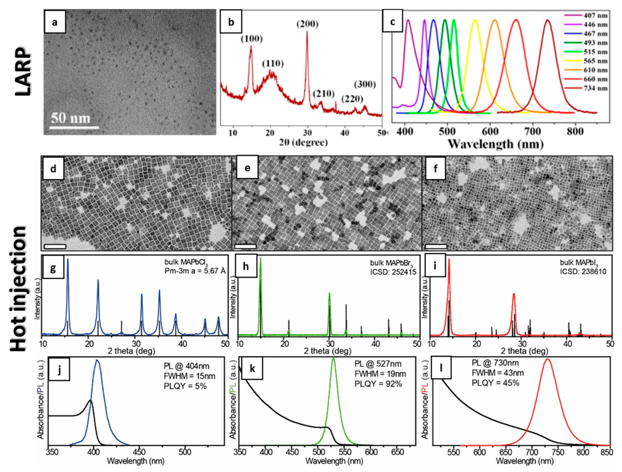
Figure 3.
(a,b) CsPbX3 NCs synthesized by LARP reproduced with permission from Ref. [19], Copyright (2016) American Chemical Society: (a) Bright field TEM image and (b) XRD pattern of CsPbX3 NCs. (c–k) CsPbX3 NCs synthesized by hot injection method reproduced with permission from Ref. [17], Copyright (2018) American Chemical Society. Bright field TEM images (scale bars are 100 nm in all images), XRD patterns of highly oriented NCs, along with absorption and PL spectra of CsPbCl3, CsPbBr3, and CsPbI3 NCs respectively.

Figure 4.
(a–d) FAPbX3 NCs synthesized by LARP reproduced with permission from Ref. [38], Copyright (2017) American Chemical Society. (a) Cubic (FAPbBr3, Pm-3m space group), (b) bright field TEM image of FAPbBr3 NCs and (c) XRD pattern of FAPbX3 NCs. (d) Photographs of FAPbX3 NCs and their optical properties along with size dependent band gap variation for FAPbBr3 NCs. (e–m) FAPbX3 NCs synthesized by hot injection method reproduced with permission from Ref. [17], Copyright (2018) American Chemical Society: Bright field TEM images (Scale bars are 100 nm in all images), XRD patterns, along with absorption and PL spectra of FAPbCl3, FAPbBr3, and FAPbI3 NCs respectively.
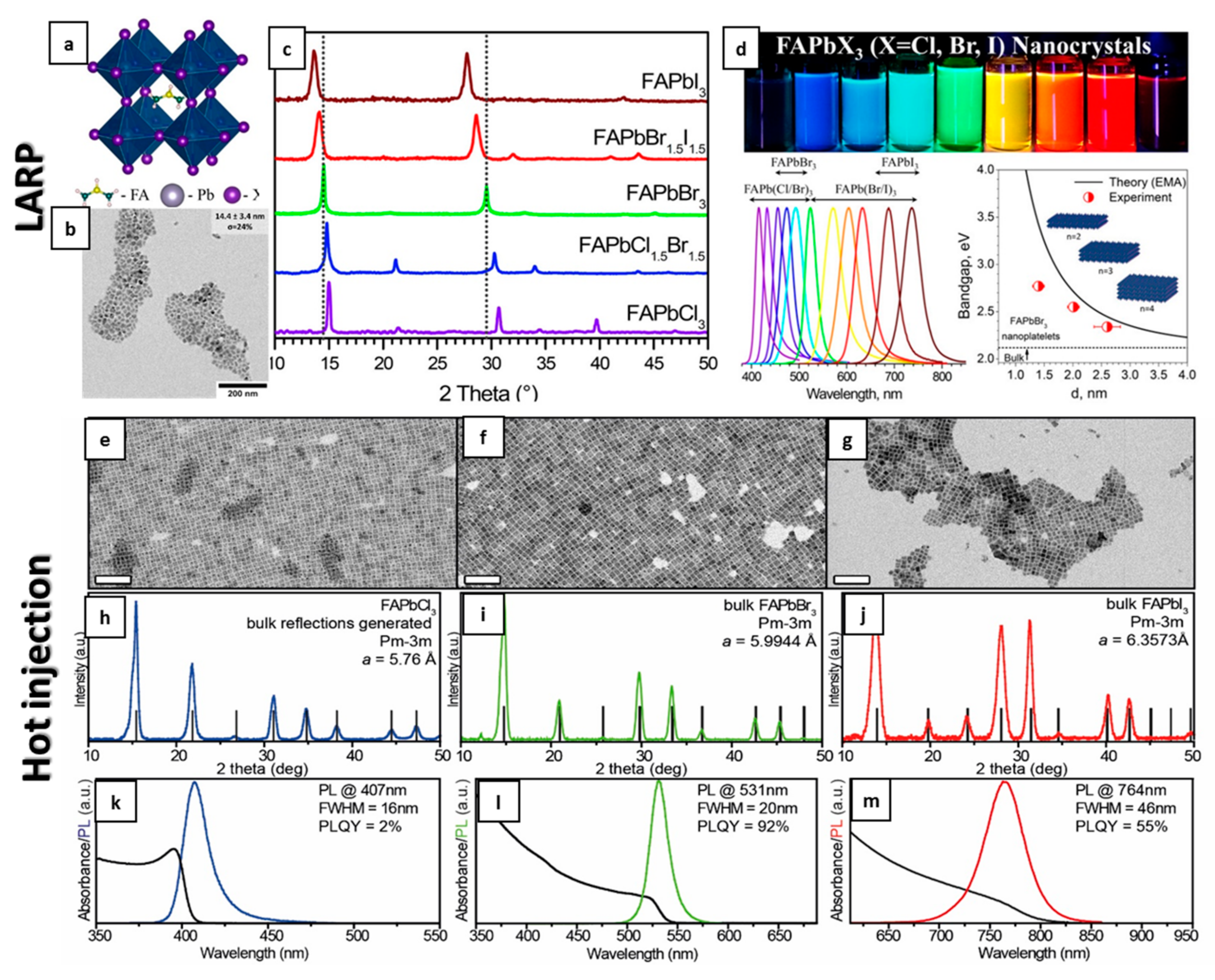
Figure 5.
(a) Evolution of the PL spectra of CsPbBr3 NCs by the addition of benzoyl chloride or benzoyl iodide. (b) Photograph of the different CsPbX3 NC solutions obtained by anion exchange under an ultraviolet (UV) lamp. (c) Evolution of the absorbance spectra of representative anion-exchanged NCs. (d) XRD patterns of the pristine CsPbBr3 NCs and the anion-exchanged samples, reproduced with permission from Ref. [17], Copyright (2018) American Chemical Society.
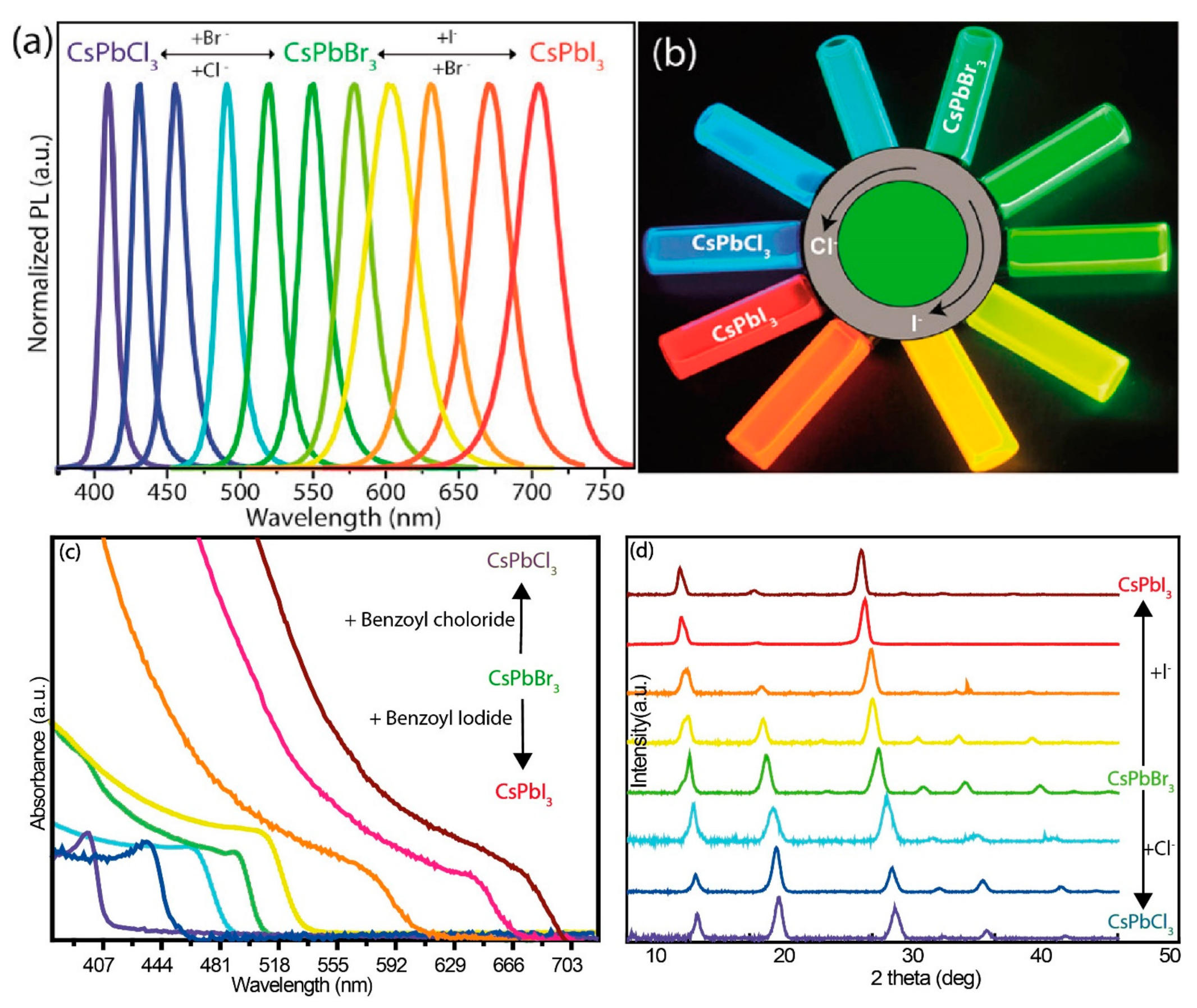
Figure 6.
Unit cells of several types of lead-free halide perovskites: (a) CsSnBr3 (inorganic crystal structure database (ICSD): 4071, cubic), (b) Cs2SnI6 (ICSD: 250743, cubic), (c) Cs3Sb2Br9 (ICSD: 39824, hexagonal) or Cs3Bi2Br9 (ICSD: 1142, hexagonal) (The atomic models are built by VESTA [54]).
Figure 6.
Unit cells of several types of lead-free halide perovskites: (a) CsSnBr3 (inorganic crystal structure database (ICSD): 4071, cubic), (b) Cs2SnI6 (ICSD: 250743, cubic), (c) Cs3Sb2Br9 (ICSD: 39824, hexagonal) or Cs3Bi2Br9 (ICSD: 1142, hexagonal) (The atomic models are built by VESTA [54]).
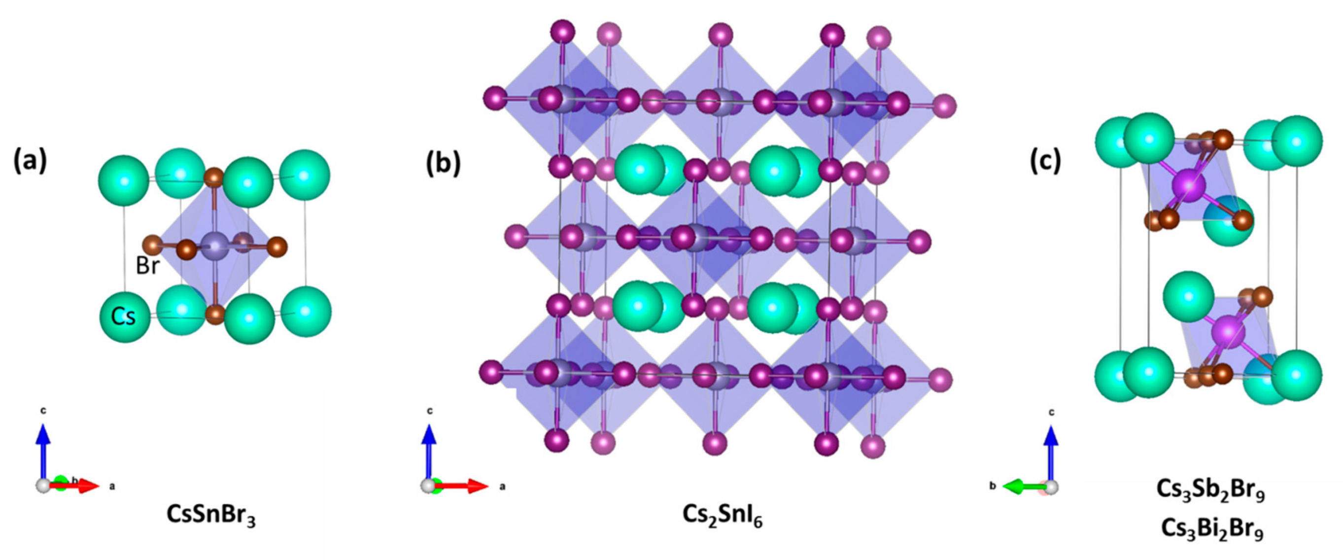
Figure 7.
(a) Powder X-ray diffraction spectra of CsSnX3 (X = Cl, Cl0.5Br0.5, Br, Br0.5I0.5, I) perovskite NCs. (b) Absorbance and steady-state PL of NCs containing pure and mixed halides. The PL spectrum of CsSn(Cl0.5Br0.5)3 particles was identical to the pure chloride-containing NCs. (c) TEM image of CsSnI3 NCs. Reproduced with permission from Ref. [55], Copyright (2016) American Chemical Society.
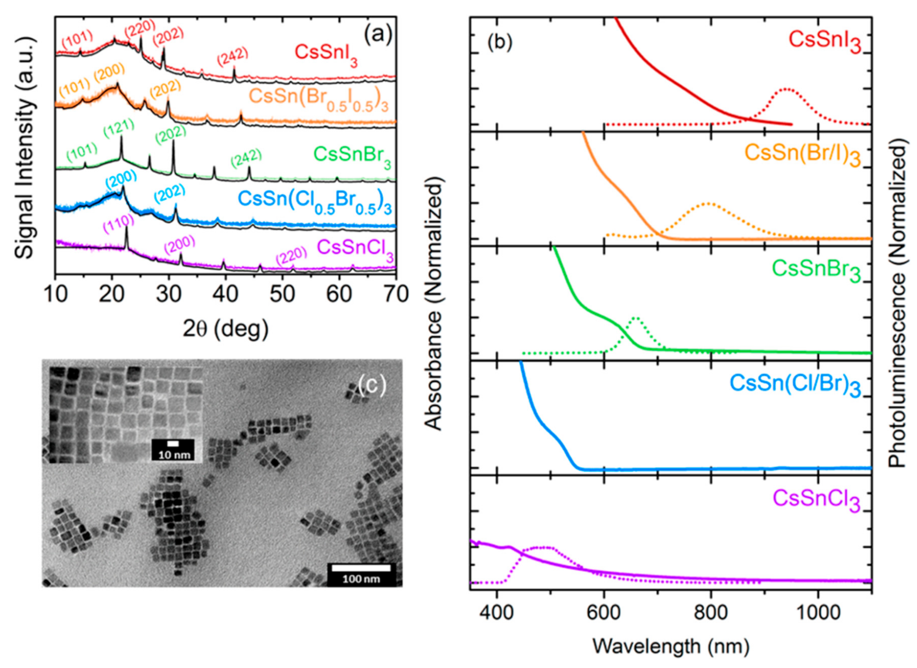
Figure 8.
Characterizations of Cs3Bi2Br9 QDs. (a) TEM image. (b) High-resolution TEM (HRTEM) image of a typical QD. (c) XRD patterns of QD powder. (d) Absorption and PL spectra. Insets: Typical optical images of the QD solution in ambient under a 325 nm UV lamp illumination. Reproduced with permission from Ref. [60], Copyright (2017) John Wiley and Sons.

Figure 9.
(a) XRD pattern of Cs2AgBiBr6 NCs synthesized at 200 °C. (b) Crystal structure of cubic Cs2AgBiBr6. (c) TEM image of Cs2AgBiBr6 NCs, (d) UV-Visible spectra of colloidal Cs2AgBiBr6 NCs, and the inset shows the Tauc plots. Reproduced with permission from Ref. [64], Copyright (2018) John Wiley and Sons.

Figure 10.
Schematic of fabrication of large crystals by antisolvent method. (a) The speed-time profile for the spin coating process with and without the various anti-solvent (A.S.T.) Optical micrographs (OM) illustrating oriented growth of needle shaped crystals with distinct size variation before thermal annealing as a function of various antisolvents with (b–g) and without A.S.T. (h) Scale bar: 300 μm. Reproduced with permission from Ref. [74].

Figure 11.
Schematics of the inter-diffusion approach and solvent vapor annealing to increase grain size. (a) The deposed PbI2 and MAI two layers by spin-coating. (b) Solvent vapor annealing using DMF vapor. (c) The formed high quality film with large grains. Reproduced with permission from Ref. [80].

Figure 12.
Top view of the scanning electron microscope (SEM) images of (a) MAPbI3 and (b) MABr-treated MAPbI3 films. Scale bars, 1 μm. Comparison of (c) ultraviolet–visible (UV-vis) absorption spectra and (d) XRD patterns of MAPbI3 films with and without MABr treatment. Reproduced with permission from Ref. [81].

Figure 13.
Procedure of single-crystal perovskite thin films using geometrically confined lateral crystal growth with a rolling module. (a) General process of the film fabrication. (b) Schematic of solvent evaporation by thermal heating. (c) Schematic of crystal growth direction. (d) The perovskite single crystal structure. Reproduced with permission from Ref. [83].

Figure 14.
Schematic illustration of inter-connected two neighbouring grain structures by additives. Reproduced with permission from Ref. [86].
Figure 14.
Schematic illustration of inter-connected two neighbouring grain structures by additives. Reproduced with permission from Ref. [86].

Figure 15.
(a) Schematic of process of vapor assisted large crystal growth and (b–d) SEM of the film after treatment with different time. Reproduced with permission from Ref. [87].
Figure 15.
(a) Schematic of process of vapor assisted large crystal growth and (b–d) SEM of the film after treatment with different time. Reproduced with permission from Ref. [87].
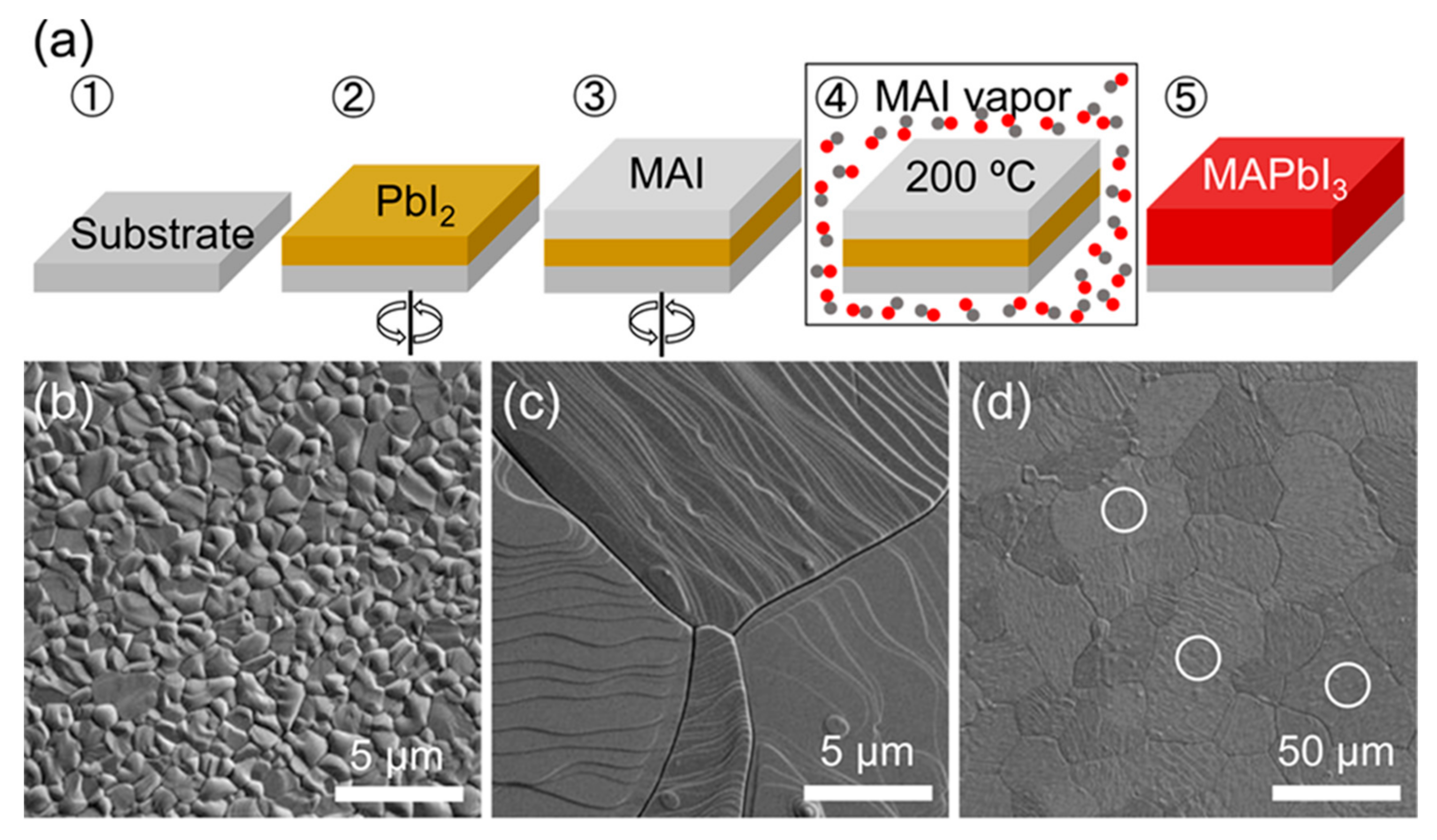

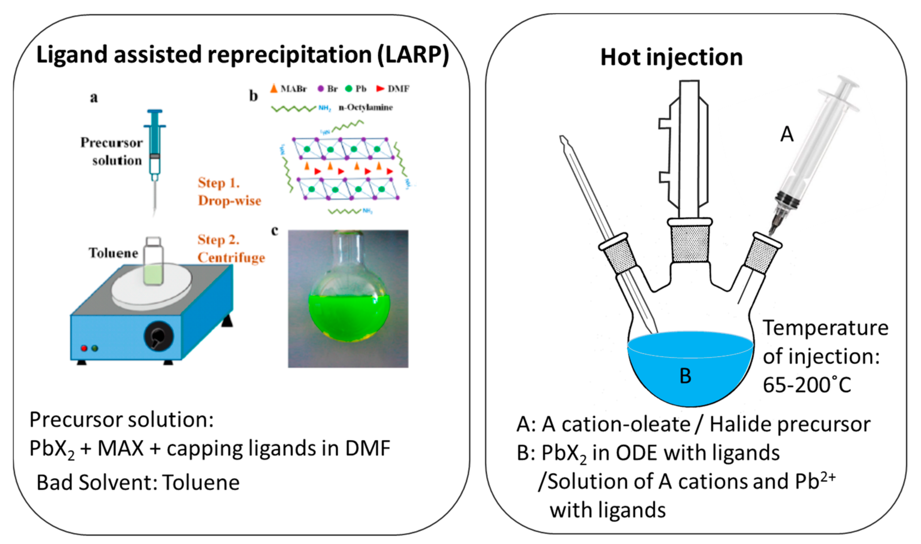
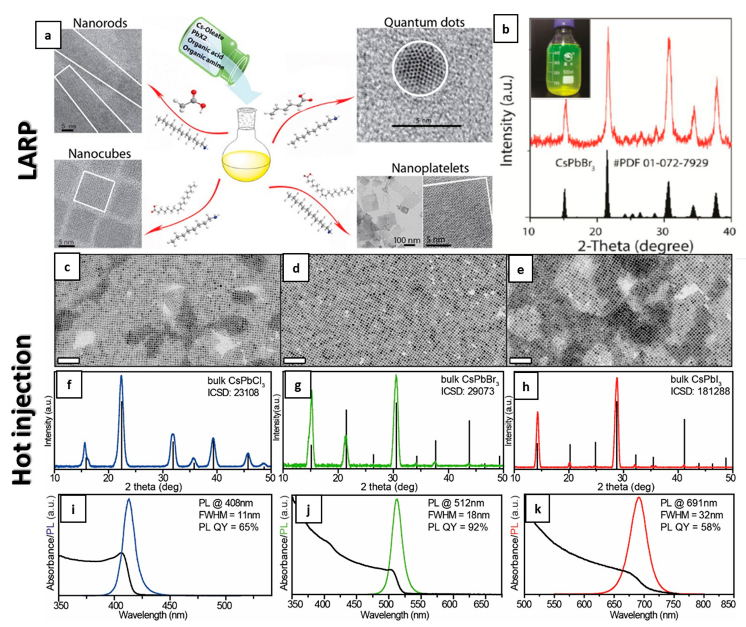
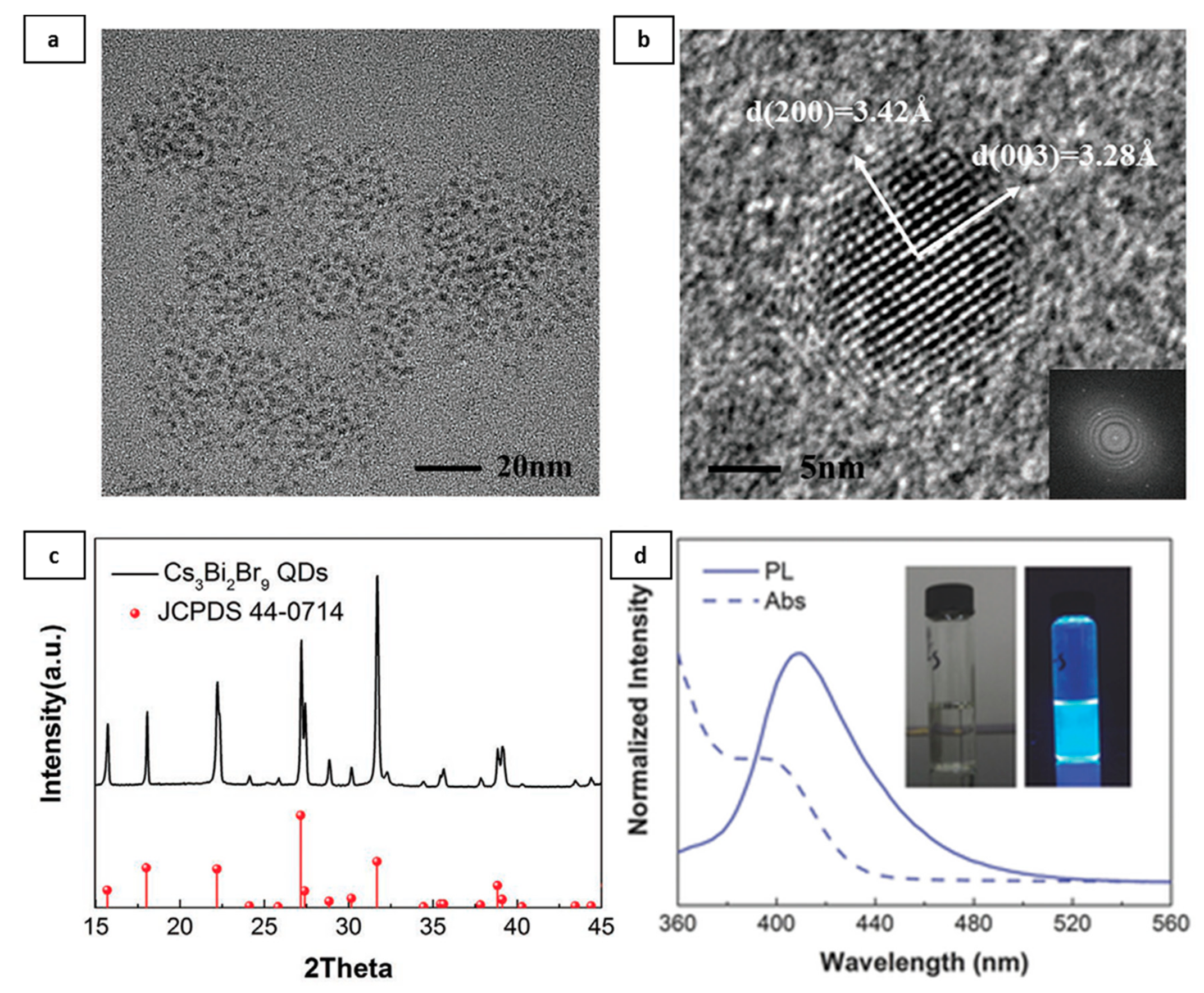
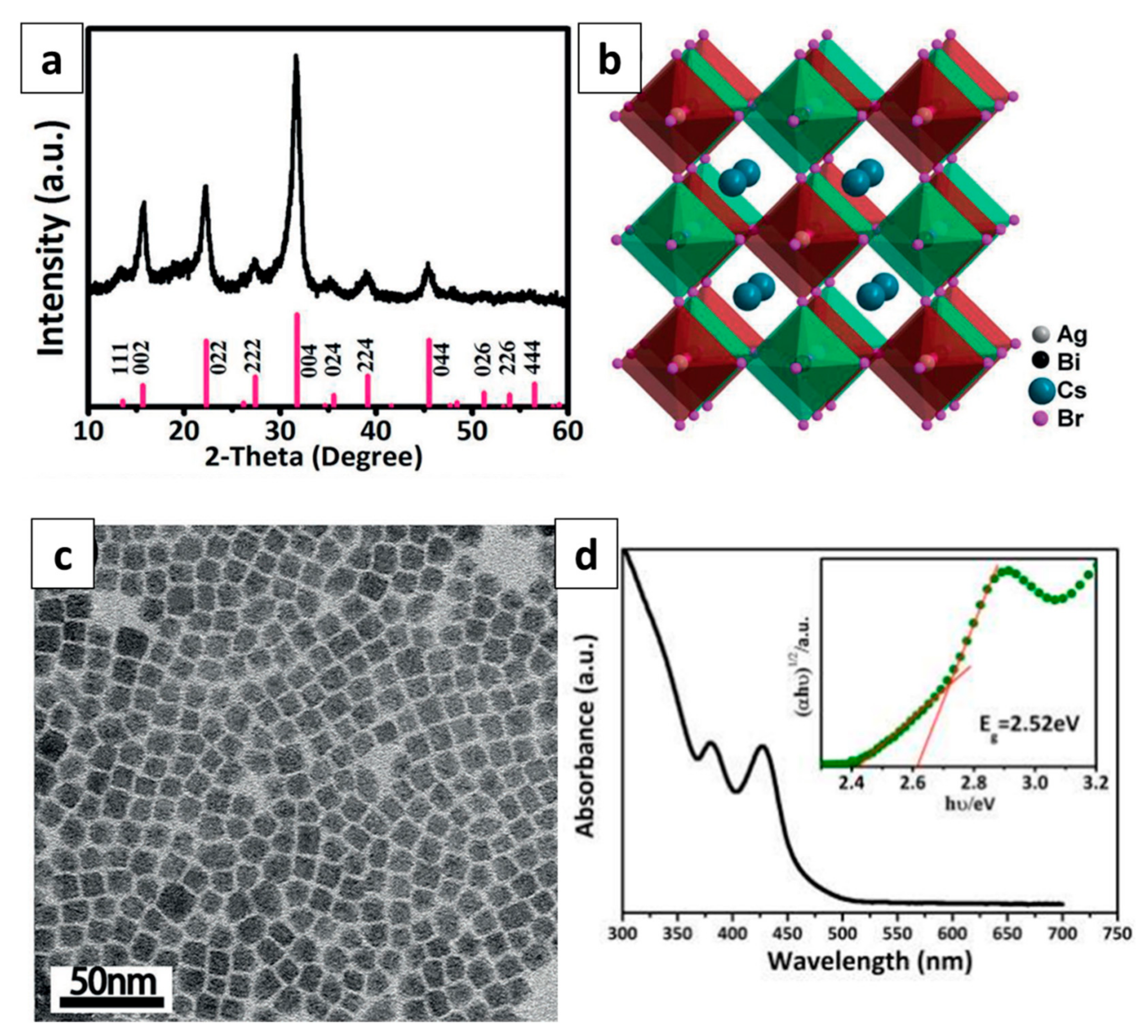
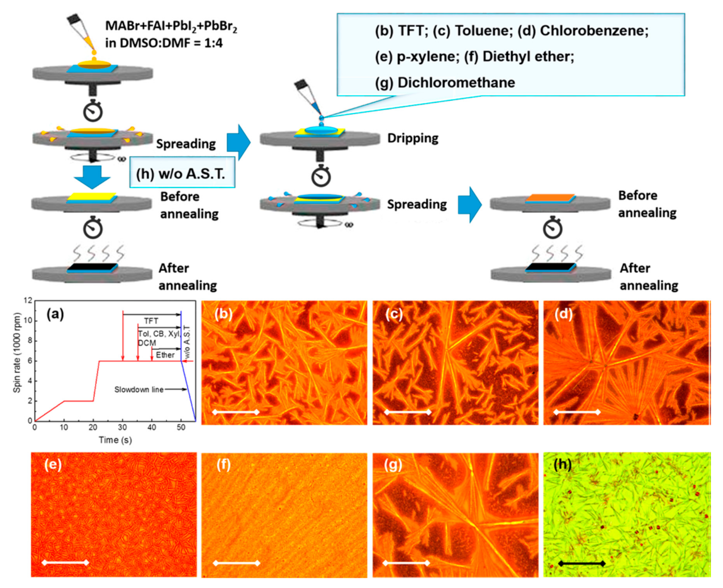
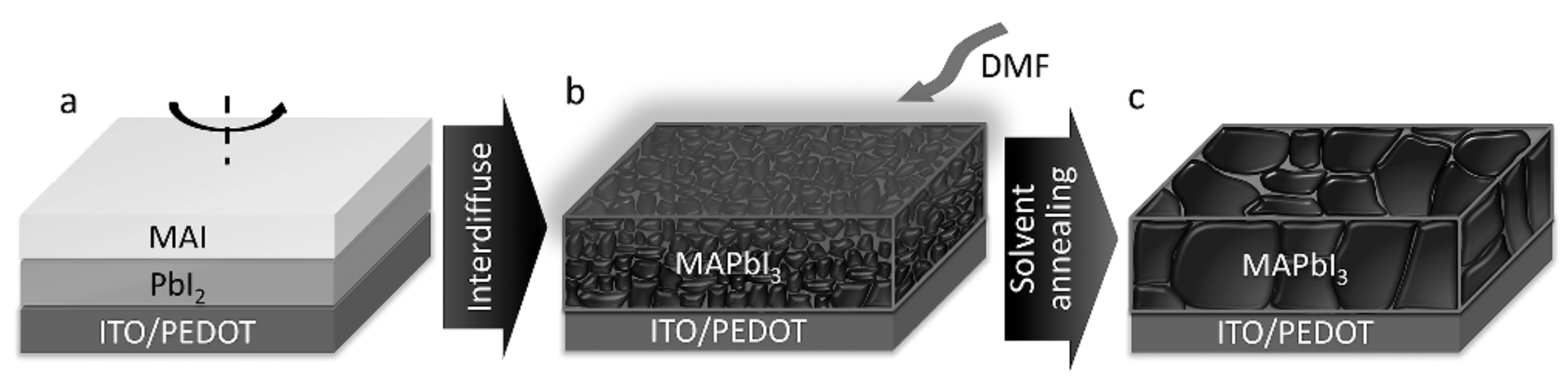
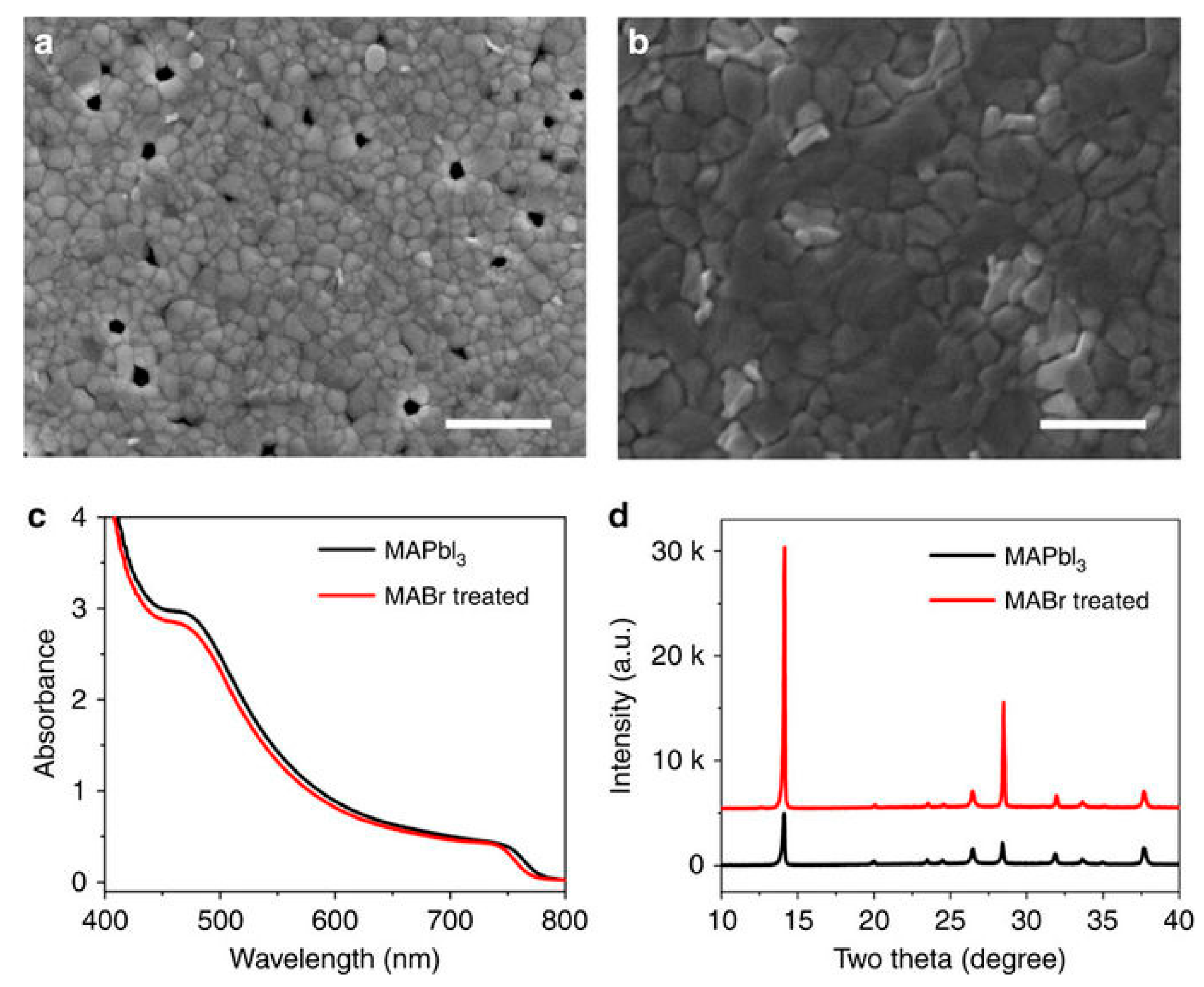
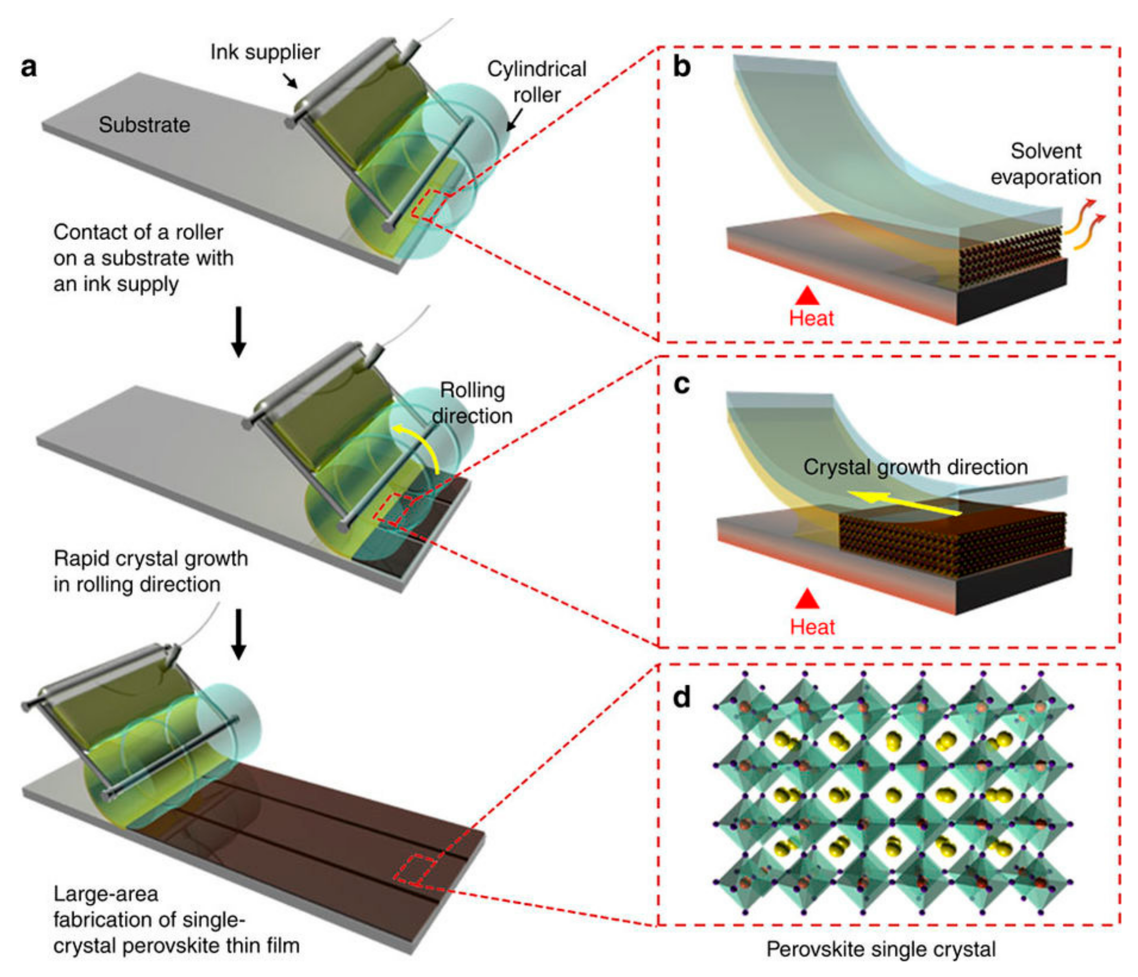
Table 1.
Summary of lead-free halide perovskite NCs from literature.
| Type of Material | Synthesis Method | Morphology | Reference |
|---|---|---|---|
| CsSnX3 (X = Cl, Br, I) | Hot injection | Nanocubes (about 15 nm) | [55] |
| Cs2SnI6 | Hot injection | quasi-spherical diameters between 35 and 80 nm | [56] |
| Cs2SnI6 | Hot injection | spherical QDs, nanorods, nanowires, and nanobelts to nanoplatelets | [57] |
| MA3Bi2Br9 | LARP | QDs with 3.05 nm ± 0.9 nm | [58] |
| Cs3Bi2X9 (X = Cl, Br, I) | LARP | QDs with 3.88 nm ± 0.67 nm | [59] |
| Cs3Sb2Br9 | LARP | QDs with 3.07 ± 0.6 nm | [60] |
| Cs2AgBiX6 (X = Cl, Br, I) | Hot injection | Nanocubes (edge length about 8 nm) | [61] |
| Cs2AgBiBr6 | Hot injection | Nanocubes (edge length about 9 nm) | [62] |
© 2018 by the authors. Licensee MDPI, Basel, Switzerland. This article is an open access article distributed under the terms and conditions of the Creative Commons Attribution (CC BY) license (http://creativecommons.org/licenses/by/4.0/).
Share and Cite
MDPI and ACS Style
Ma, H.H.; Imran, M.; Dang, Z.; Hu, Z. Growth of Metal Halide Perovskite, from Nanocrystal to Micron-Scale Crystal: A Review. Crystals 2018, 8, 182. https://doi.org/10.3390/cryst8050182
AMA Style
Ma HH, Imran M, Dang Z, Hu Z. Growth of Metal Halide Perovskite, from Nanocrystal to Micron-Scale Crystal: A Review. Crystals. 2018; 8(5):182. https://doi.org/10.3390/cryst8050182
Chicago/Turabian StyleMa, Haijiao Harsan, Muhammad Imran, Zhiya Dang, and Zhaosheng Hu. 2018. "Growth of Metal Halide Perovskite, from Nanocrystal to Micron-Scale Crystal: A Review" Crystals 8, no. 5: 182. https://doi.org/10.3390/cryst8050182
Note that from the first issue of 2016, this journal uses article numbers instead of page numbers. See further details here.