1. Introduction
A choice of growth substrate for III-N based technology is directed most often by the cost effectiveness of the solution combined with a final quality of the device. Sapphire substrates and GaN/sapphire templates are commonly chosen, but their applicability is often limited by low thermal conductivity of sapphire (0.25–0.50 W/cm K at 100 °C [
1]). This can be avoided if the growth is performed on a SiC substrate which has superior thermal properties to sapphire (thermal conductivity of 5 W/cm K at 100 °C) [
2]. However, a higher cost and larger lattice mismatch [
3] often prevents this solution. Ideally, III-N devices should be grown on a native substrate such as GaN which can be grown by a hydride vapor phase epitaxy or the ammonothermal method. The first of those methods offers a low impurity level but suffers from wafer bow. Ammonothermal GaN boasts the highest crystalline quality in the field but unintentional doping can be a problem [
4]. Work is being done in order to combine the best qualities of both methods [
5,
6].
Ammonothermal bulk GaN crystals can be grown with an intended conductivity level by controlling the unintentional oxygen content during the growth process, leading to an electron concentration up to ~10
20 cm
−3 (n-type) and an intentional Mg concentration up to ~10
19 cm
−3 (p-type) [
7]. The ammonothermal method can also obtain semi-insulating (SI) GaN crystals which are crucial for power electronics [
8] via appropriate compensation of oxygen donors by Mg acceptors. While the possibility of obtaining conductive substrates is beneficial in some areas, the impact of introduced dopants on the transparency of the crystals can be detrimental in others. Such examples are GaN-based intersubband devices which operate in a mid-infrared spectral range [
9,
10] and thereby need substrates which are transparent in this spectral range. On the other hand, a high doping can achieve a significant refractive index contrast between the substrate and the device stack. Such doped substrates (i.e., plasmonic substrates) have been shown as effective bottom cladding for mode guiding in InGaN/GaN optoelectronic devices, including lasers operating in a visible spectral range [
11,
12].
Semi-insulating (SI) GaN is known to be transparent from 0.36 µm to ~7 µm where an absorption on a second harmonic of optical phonons occurs [
13,
14,
15]. This broad transparency window allows fabrication of optical devices which operate outside the typical spectral range (e.g., at 1.55 µm) related with III-N structures (i.e., structures which emit UV, blue, and green light). In order to achieve emission at such low energies, intersubband transitions are used. Several devices operating on this principle have already been proposed [
9,
10]. However, several factors can influence the transparency of GaN in the infrared range. It has been shown that GaN grown on sapphire and SiC (i.e., GaN/sapphire and GaN/SiC templates) has a narrower transparency window [
14]. The use of additional substrates (in this case sapphire and SiC) leads to a shift of the long wavelength cut-off due to non-transparency of these substrates. Another, rather well known, mechanism leading to absorption in the infrared region is the introduction of free carriers. An introduction of 10
19 cm
−3 electrons by O doping shifts the cut-off from ~7 µm to well below 2 µm [
14]. There is, however, no systematic study showing the dependency of the cut-off position on the carrier concentration including n- and p-type doping. In [
14], only semi-insulating and highly doped (n ~ 10
19 cm
−3) bulk GaN substrates were compared to unintentionally doped GaN layers grown on sapphire and SiC.
In the 7–14 µm window (excluding the narrow 9–10 µm) GaN is not transparent due to an absorption on the Restrahlen band [
13]. However, at longer wavelengths, the radiation should be able to penetrate the material. It is especially interesting to study this in the context of growing interest in terahertz imaging. III-N based devices have been shown to be suitable for detection and emission of terahertz waves. Devices based on an intraband absorption in quantum wells [
16,
17] or plasma wave excitation [
18] have been presented. However, the transparency of GaN crystals in the terahertz range has not been studied yet.
While the transparency window of SI GaN is 0.36–7 µm, doping can significantly affect it not only in the infrared and at longer wavelengths, but also in the visible range. This is unfavorable from the optoelectronics point of view where a reabsorption of the light emitted from an active part of the device (i.e., a quantum well) can occur in the doped passive part (e.g., a contact layer). In this way, a significant part of the emission may be blocked.
In this paper we analyze the optical transparency of SI and doped ammonothermal GaN substrates in the near-infrared, mid-infrared, and terahertz spectral range. In particular, we analyze the effect of doping on the blueshift of the cut-off wavelength in the mid-infrared region. Semi-insulating substrates and n-type doped crystals with doping concentration in the range from 4.4 × 10
17 cm
−3 to 9 × 10
19 cm
−3 are examined significantly extending the work done in [
14]. The influence of p-type doping on the cut-off wavelength shift is also analyzed. In the terahertz range, the loss of transparency due to the doping is studied. In addition, we show how the absorption coefficient is affected by the carrier concentration in the visible and near-infrared region where GaN crystals are quite transparent.
3. Results and Discussion
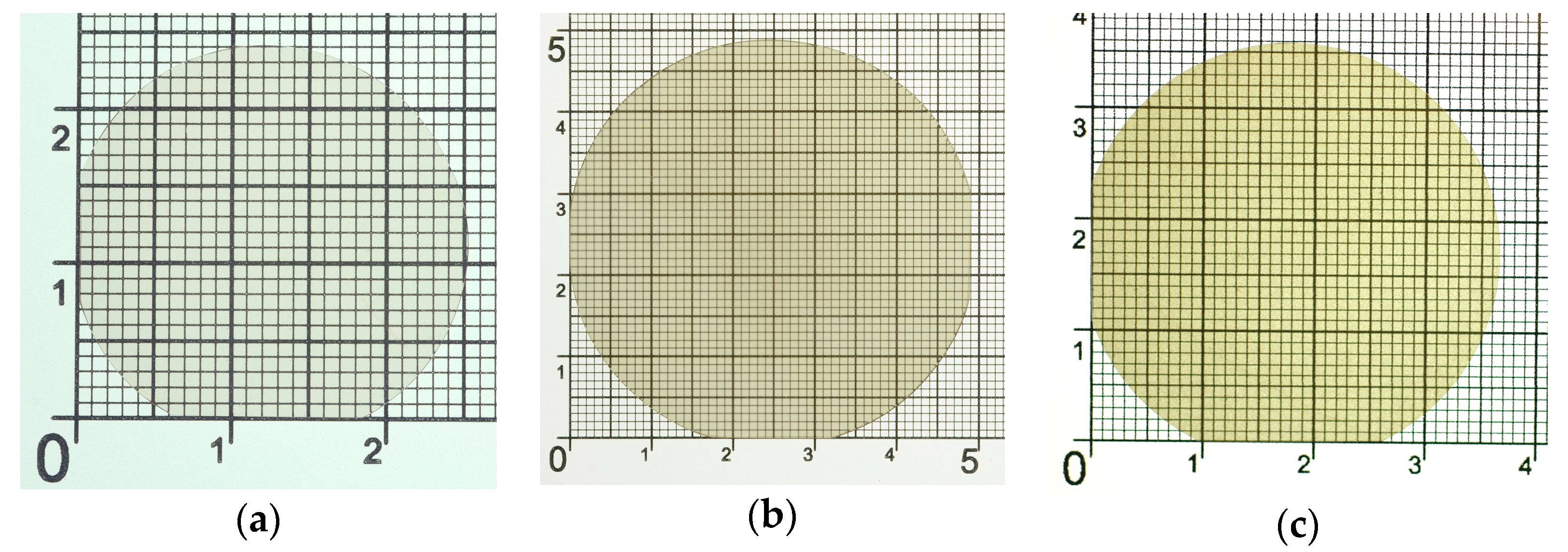
Figure 1 shows 1 inch low n-type highly transparent GaN, 2 inches n-type (
n = 10
19 cm
−3) GaN and 1.5-inch SI GaN substrates of polar orientation produced by the Ammono company. They can be prepared in an epiready standard for both Ga- and N-polar sides and their conductivity can be controlled from n-type to p-type. Such 2 inch and 1 inch substrates are widely used for fabrication of AlGaN/GaN transistors (SI substrates) and InGaN/GaN lasers (n-type substrates). As seen with the naked eye, they are very well transparent in the visible spectral range. However, the transparency of GaN is changing with the increase in the doping concentration and in the visible spectral range it can be seen with the naked eye, see
Figure 2 which shows n-type and p-type GaN samples with various doping concentrations and the change of color due to the doping. These ammonothermal GaN crystals are the subject of studies of transparency in the near-infrared, mid-infrared, and THz spectral range. In addition, for n-type substrates, which are widely used in light emitters operating in the visible spectral range, the absorption coefficient is determined in this spectral range.
Figure 3a shows transmission spectra measured at room temperature for GaN crystals doped by oxygen with various concentrations of free electrons. A spectrum recorded for a SI GaN is included as a reference. A gradual decrease of transparency is visible with an increase in free carrier concentration and the cut-off wavelength shifts towards shorter wavelengths. To illustrate the influence of the carrier concentration on the transparency wavelengths corresponding to 30% and 10% transparency are plotted in
Figure 3b. The cut-off wavelength shifts linearly towards the visible range on a semi-logarithmic plot. This effect is attributed to absorption on free carriers as all dopants are ionized at room temperature as schematically shown in the sketch in
Figure 3b. This feature could be used to tune the transparency of GaN in the 1–7 µm spectral range.
In general, the free carrier absorption is a well-known phenomenon in semiconductors which has been also observed for n-type GaN [
13,
14,
15,
20,
21,
22]. In order to compare our experimental results with a quantitative analysis, the plasma frequency (
ωP) has been calculated for various carrier concentrations according to Equation (2)
where
n and
e are the free electron concentration and the elementary charge, respectively,
m∗ is the effective electron mass which is assumed to be 0.22
m0 (
m0 is the electron rest mass) [
23],
ε∞ is the high frequency limit of the dielectric constant assumed 5.35, and
ε0 is the vacuum dielectric constant. The calculated plasma frequency is plotted in
Figure 3b by a solid black line. In addition, the mode of high energy branch of longitudinal phonon-plasmon (LPP
+) is plotted by a dashed red line in
Figure 3b. This mode is calculated according to the following formula
where
ωLO and
ωTO are the zero carrier density frequencies of the
E1 longitudinal (LO) and transversal optical (TO) phonon frequencies [
14].
For a low electron concentration (
n < 10
17 cm
−3), the transparency of a GaN substrate in the mid-infrared region ends at ~6.8 μm, which is labeled as 2
ωLO in
Figure 3 and corresponds to the second harmonic LO phonon generation in GaN. The strong absorption ends at the energy corresponding to two TO phonons which is labeled as 2
ωTO in
Figure 3. It is worth noting that, for zinc-blended semiconductors, such as GaAs or InP, the second-harmonic absorption is negligibly weak. In the case of GaN, this absorption is very strong since the
E1 LO and TO mode is polarized transverse to the c axis similarly like the incident radiation. Next, a window of sample transparency is observed in the ~9–10 µm range and no transparency is observed above 10 µm for the SI sample. An absorption due to the first harmonic LO phonon generation in GaN is expected at longer wavelengths (the energy of a LO phonon corresponds to ~13.5 µm), but this absorption can be significantly broadened due to phonon-phonon scattering [
13] and/or can be attributed to LPP
+, see dashed red line in
Figure 3b. In this figure, it is also visible that the transparency window, see green arrow in
Figure 3b defined between LPP
+ and 2
ωTO, is narrowing with the increase in electron concentration. Above the electron concentration
n > 2 × 10
17 cm
−3 this window reduces to zero. With the next increase in electron concentration, the cut-off for transparency shifts to a shorter wavelength due to a free carrier absorption (black solid line) and the LPP
+ absorption. These theoretical predictions are very consistent with experimental data which corresponds to 30% (red open squares) and 10% (blue open squares) transparency of the sample. In addition, it is visible that the mid-infrared absorption edge becomes sharper with the increase in electron concentration, compare slopes of the absorption edge in
Figure 3a or the spectral positon of red and blue squares in
Figure 3b. Summarizing this analysis, it is clearly visible that the transparency of n-type GaN substrates in the near and mid infrared region is controlled by the electron concentration and the wavelength cut-off is very well described by the plasma frequency for
n > 1 × 10
18 cm
−3. The scenario is different for p-type GaN.
Figure 4a shows transmission spectra measured for GaN crystals doped with Mg. At 1 × 10
18 cm
−3 doping level, the transparency curve has a similar shape to that of SI GaN and the cut-off frequency stays at the same position. The notable difference appears at wavelengths <6 µm where a significant drop of transparency is visible. At ~0.2 eV (6.2 µm) and higher this drop corresponds to the energy needed to excite electrons from the valence band (VB) to the Mg acceptor level, as schematically shown in the sketch in
Figure 3b. An increase in doping concentration to 5 × 10
18 cm
−3 leads to a strong decrease of the transparency of the whole infrared range. Since the free hole absorption is expected to be negligibly important in this spectral range in these samples due to a low hole concentration and a large effective mass for holes in GaN, this absorption is attributed to optical transitions between (i) the VB and Mg-related acceptors, (ii) dopants (Mg-related acceptors and non-intentional donors (both deep and shallow)), (iii) occupied Mg acceptors and the conduction band (CB), and (iv) the VB and deep donors which are unoccupied by electrons in Mg-doped GaN. These processes are schematically illustrated in
Figure 4b and their intensities/significance vary with the Mg concentration in GaN crystals as well as the concentration of non-intentional donor dopants. A quantitative analysis in this case is difficult, since the model of the defect absorption is not well established for GaN. However, it is possible to estimate the wavelength cut-off which is related to the free hole plasma frequency. For a hole concentration
p = 10
18 cm
−3 the cut-off is expected at ~9 µm, i.e., at much longer wavelengths than this for which no transparency is observed for GaN:Mg samples with Mg concentration ≥5 × 10
18 cm
−3.
Since the activation energy of Mg dopants in GaN is large (~170 meV [
24]), the nature of the transparency of p-type GaN is different than this one which takes place in n-type GaN where the activation energy of O donors is comparable with the thermal energy at room temperature (the activation energy of oxygen in GaN is ~29–32 meV [
25,
26,
27]). Even if non-intentional deep donors are present in n-type GaN, the free carrier absorption determines the transparency of n-type GaN in the infrared spectral region. In such a case, optical transitions between deep donors and the CB are also expected but their significance is negligible if the electron concentration is high enough, e.g., >3 × 10
18 cm
−3 as seen in
Figure 3a.
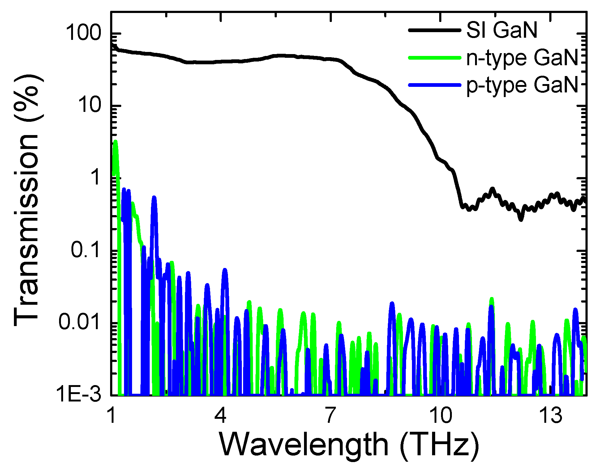
Figure 5 shows transmission spectra measured in the terahertz range (1–14 THz) for SI, n-type with the electron concentration on the level of 10
18 cm
−3, and p-type with the Mg doping level of 10
18 cm
−3 GaN crystals. The SI GaN crystal shows ~50% transparency in 1–8 THz range which then drops to below 1% at 10 THz and higher. The drop starting at 8 THz corresponds to the activation energy of ~32 meV of O
N (oxygen substituting nitrogen) defect in GaN which acts as a shallow donor [
27]. At room temperature (26 meV), only a part of O
N donors are thermally activated. Remaining inactivated impurities can absorb radiation to release electrons to the conduction band. Since there is a significant amount of oxygen, even in SI GaN crystals grown by ammonothermal method, such an effect is expected and we attribute the drop in transparency at frequencies >8 THz to the absorption on oxygen impurities. The result shows that GaN is a suitable material for applications in 1–8 THz and can be considered for use in 8–14 THz only if the structure is thin (so the absorption is kept low) and the GaN-based structure is fabricated on a suitable substrate which is also transparent in the terahertz range. On the other hand, doping makes GaN completely non-transparent in the terahertz range with transmission below 0.1%. This effect is present for both n- and p-type doping. It is expected that the transparency of GaN in the THz spectral range can be tuned via n- or p-type doping below 10
18 cm
−3 but quantitative analysis of this issue needs samples with suitably low unintentional impurity concentration. Moreover, it is worth noting that SI GaN can be obtained via co-doping, i.e., O dopants can be compensated by Mg dopants etc. This suggests that the transparency of SI GaN in the THz spectral range can be also tuned. Such an effect was observed for SI GaN crystals obtained by the ammonothermal method. We believe that further studies of transparency of GaN in the THz spectral range require samples with low non-intentional doping, i.e., below <10
17 cm
−3.
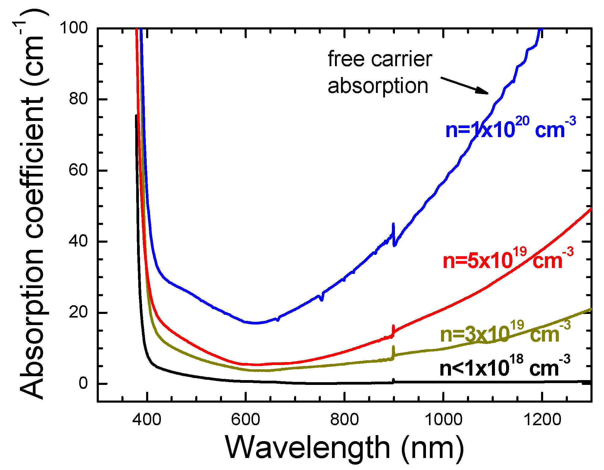
Since conductive GaN substrates are needed for the fabrication of light emitting diodes and laser diodes emitting in the visible (blue-green) spectral range, it is important to know how small the absorption coefficient is at these wavelengths for n-type GaN substrates typically used for production of laser diodes.
Figure 6 shows the absorption coefficient (α) determined for such substrates in the visible and near-infrared region. Below 400 nm, the sharp increase in absorption is observed because of the Urbach tail of density of states in the conduction band (O-related donor states). At
n < 1 × 10
18 cm
−3 carrier concentration the absorption coefficient is as low as 2–3 cm
−1 at 450 nm and stays on this level in the whole 450–1200 nm range. An increase in carrier concentration to 3 × 10
19 cm
−3 and higher causes α to increase as well. The change is lowest at around 630 nm and most pronounced in the infrared. While the performance of blue and green laser diodes may be affected by partial absorption of light in doped layers, this influence might be avoided by reducing the thickness of the aforementioned layers. In infrared, however, α reaches a value of ~100 cm
−1. This can significantly impede the efficiency of intersubband GaN-based emitters. Suitable steps must be taken in order to avoid this effect.
Transparency of p-type GaN in the visible spectral range is significantly affected by a dopant-related absorption which was previously discussed. This phenomenon is observed with the naked eye in
Figure 2 for p-type samples. Therefore, p-type GaN substrates are less interesting for light emitters operating in blue-green spectral range and the absorption coefficient in visible spectral range is not analyzed in this paper. In general, the sharp decrease in transparency due to doping is a well-known phenomenon for Mg-doped GaN in light emitters since the top cladding is p-type and can significantly absorb the light emitted from the InGaN/GaN quantum well region. In order to minimize this effect, the thickness of the Mg-doped layer is reduced as much as it is possible and hence the p-type layer is more transparent. GaN crystals shown in
Figure 2 are ~0.5 mm thick and therefore transparency of p-type samples with larger Mg concentration is very poor in this case but it improves with the reduction of substrate thickness.

 ,
, 


