Review

Progress in Indentation Study of Materials via Both Experimental and Numerical Methods

1
Department of Materials Engineering, The University of Tokyo, 7-3-1 Hongo, Bunkyo-ku, Tokyo 113-8656, Japan
2
School of Mechanical, Materials and Mechatronic Engineering, University of Wollongong, Wollongong, NSW 2522, Australia
3
School of Mechanical & Aerospace Engineering, Nanyang Technological University, 50 Nanyang Avenue, Singapore 639798, Singapore
*
Authors to whom correspondence should be addressed.
Crystals 2017, 7(10), 258; https://doi.org/10.3390/cryst7100258
Submission received: 19 June 2017 / Revised: 8 August 2017 / Accepted: 9 August 2017 / Published: 13 October 2017
(This article belongs to the Special Issue Crystal Indentation Hardness)

Abstract

:
Indentation as a method to characterize materials has a history of more than 117 years. However, to date, it is still the most popular way to measure the mechanical properties of various materials at microscale and nanoscale. This review summarizes the background and the basic principle of processing by indentation. It is demonstrated that indentation is an effective and efficient method to identify mechanical properties, such as hardness, Young’s modulus, etc., of materials at smaller scale, when the traditional tensile tests could not be applied. The review also describes indentation process via both experimental tests and numerical modelling in recent studies.

1. Introduction

Indentation tests were first performed by a Swedish iron mill’s technical manager Brinell who used spherical balls from hardened steel ball bearings or made of cemented tungsten carbide as indenters to measure the plastic properties of materials in 1900 [1,2,3,4]. Brinell’s testing approach is schematically shown in Figure 1a. Brinell also proposed the following formula to determine the hardness
H B = 2 P π D ( D D 2 d 2 )
here HB is the Brinell hardness; P is the load; D is the diameter of the ball indenter and d is the diameter of residual area of the impression.
Brinell’s work was then followed and improved by Meyer in 1908 [5]. In his work, the hardness (H) is calculated by the load (P) divided by the projected area (A), namely
H = P A
In 1922, the Vickers test was carried out and commercialized by the Firth-Vickers company [6]. A square-based pyramid diamond indenter with a 136° semi-angle was used instead of a ball indenter, as shown in Figure 1b. The Vickers hardness (HV) is defined as the load divided by the surface area of the impression, namely
H V = 1.8544 P d V 2
where dV is the length of diagonal of the surface area.
The Brinell, Meyer and Vickers methods were then widely used in the metallurgical and engineering industries in the early 20th century since indentation tests offered simplicity, low-cost and high speed compared with conventional tensile testing. No special shape or extra fabrication of sample is required for indentation tests except for a simple sample with a flat surface. In addition, several indentation tests could be quickly performed on a small area without destroying the whole sample.
Another significant finding is that the hardness is load-dependent, which was proposed by Meyer through ball indentation experiments on a wide range of metals [7]. For a given ball size, the diameter of the impression after unloading was found to be related to the applied load by the following empirical relationship:
P = C d n
here P is the applied load; C is a constant of proportionality; the exponent n is the well-known Meyer index and d is the diameter of the residual area of the impression after unloading. When the n-value is less than 2, according to Equations (2) and (4), the hardness increases with decreasing the load. While the n-value is larger than 2, the hardness decreases with decreasing the load. If the Meyer index equals to 2, the hardness is a constant, namely load-independent. For most metals that can be work hardened by the indentation process, n > 2 [7]. Therefore, the Meyer index has been found to be strongly dependent on the work hardening of the tested material and to be independent of the size of the ball indenter [5]. Meyer [5] also found that the same hardness using balls of different diameters could be obtained only if the indentations were geometrically similar, namely with the same ratio d/D.
Tabor’s work [8] performed in 1948 represents a landmark in the understanding of the indentation process. He qualitatively described the procedure how an indentation by a ball initially led to elastic deformation, then to plastic flow associating with work hardening, and final on removal of the load to elastic recovery. In 1951, Tabor [1] had proven that the indentation hardness (H) could be related to the yield stress (σ) of the material by an equation based on the theory of indentation of a rigid perfectly plastic solid, namely
H = C σ
where C is a constant, which depends on the geometry of the indenters. For the strain-hardened materials and the materials which consequently have no definite yield stress, the stress measured at a representative strain εr can be used as σ [9]. The representative strain denotes the strain at where the corresponding stress can be regarded as the yield stress during tensile deformation for the materials without definite yield stress. The value of the representative strain is relevant to the geometry of the indenter. For instance, ε r 0.08 for a Vickers diamond indenter.
Tabor [7] started taking an interest in the indentation response of polymers and of macroscopically brittle materials in the studies of their frictions. In the following couple of years, Tabor and King [10] reported the method of estimating the yield pressure on polyethylene, PMMA (Polymethyl methacrylate), PTFE (Polytetrafluoroethylene), and halocarbon polymer via Vickers hardness measurements. Subsequently, Pascoe and Tabor [11] reported a range of polymers obeyed Meyer’s laws. The single-crystal rock salt was also investigated by King and Tabor [12] with Vickers indentations, by which, they found the values of yield stress from the indentation matched well with the compression experiments.
In 1960s, indentation at high temperature was investigated by Atkins and Tabor [13]. They studied the mechanical properties of single crystals of MgO at temperatures of 600 °C to 1700 °C via the mutual indentation hardness technique. It was found that the short-time hardness decreased when the temperature increased.
Conventional indentation tests have the length scale of the penetration in microns or millimetres. In the mid-1970s, the indentation technique was applied to measure the hardness of small volumes of material, such as thin film. The length scale of the penetration is usually in nanometres. Therefore, this new technique is called nanoindentation. Apart from the penetration length scale, the distinguishing feature of nanoindentation testing is the indirect measurement of the contact area [14]. In conventional indentation tests, the contact area is directly measured from the residual impression area. In nanoindentation test, the residual impression area is too small to be directly measured. Therefore, the contact area is determined by the measured penetration depth in nanoindentation.
Since 1980s, especially after 1990s, extensive experimental studies of nanoindentation have been performed on many different types of materials. This review will provide the systematic description of indentation study of materials via both experimental and numerical methods. The contents of this article can be summarized as follows. The first section provides the background necessary for understanding the mechanics of indentation and hence for understanding its applications in materials science. The second part reviews methods of mechanical properties characterization and measurement and follows with application to experimental measurement reported in the literature. Next, we discuss the numerical study of deformation mechanism of materials induced by indentation. We follow with a comprehensive review of the models involved in texture and indentation size effect prediction, ranging in length scale from the meso- and micro- to the nanoscale, and a critical assessment of their performance.

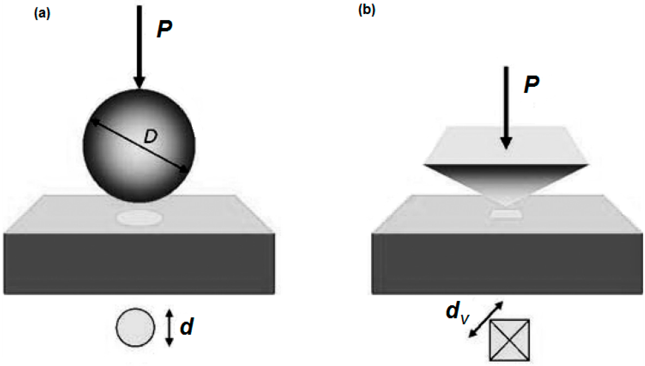
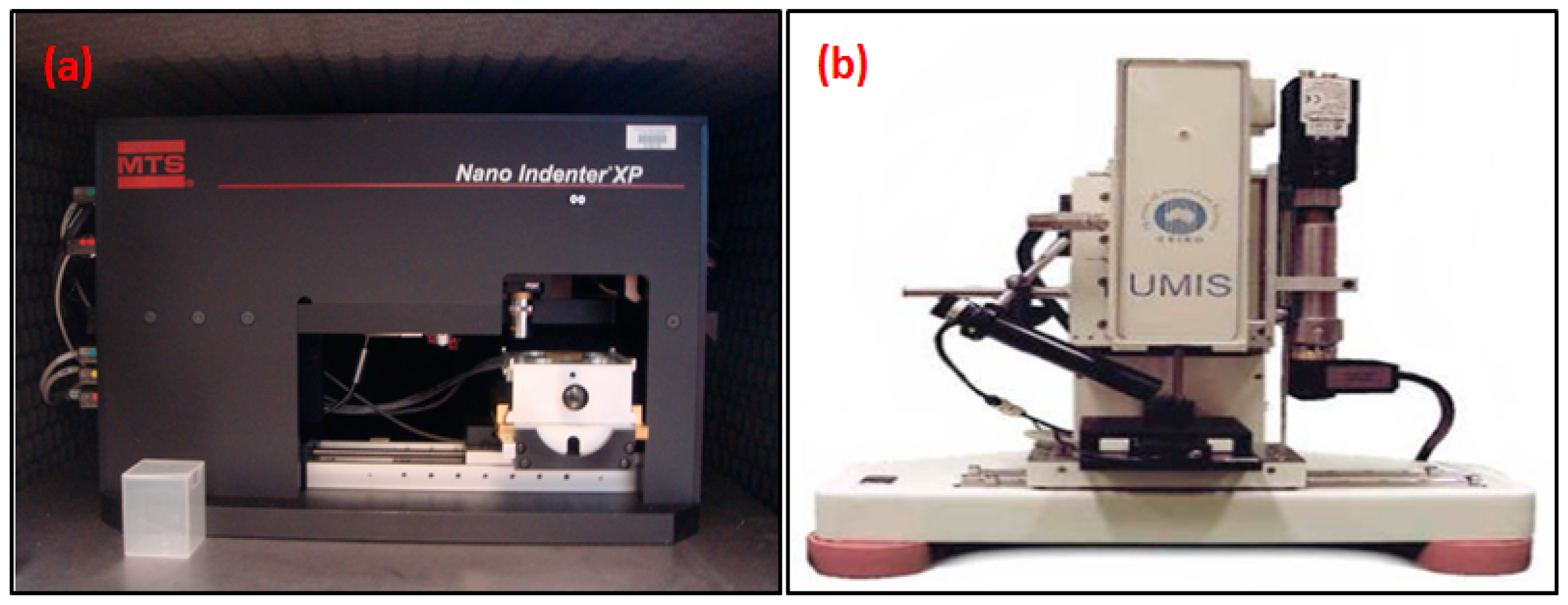
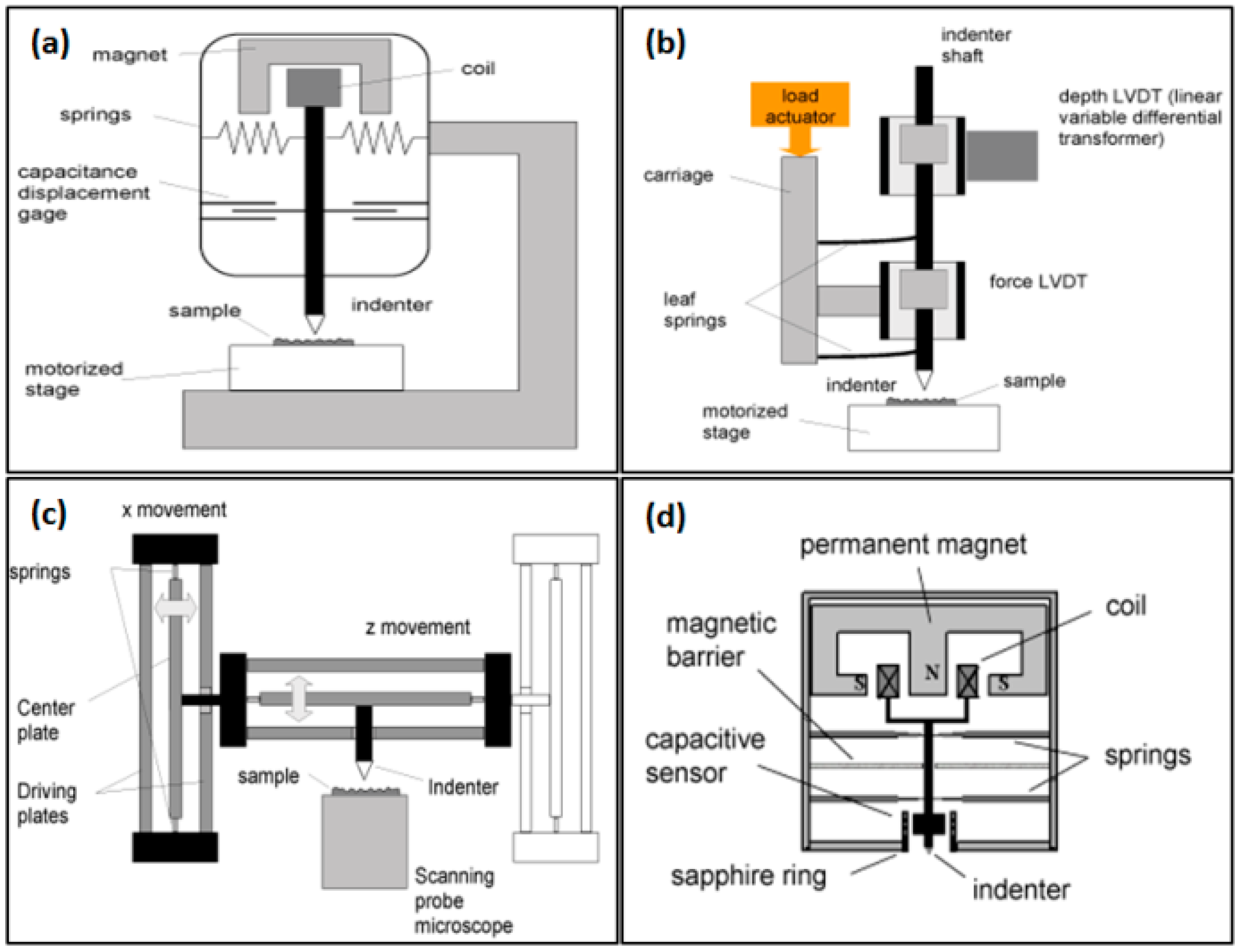
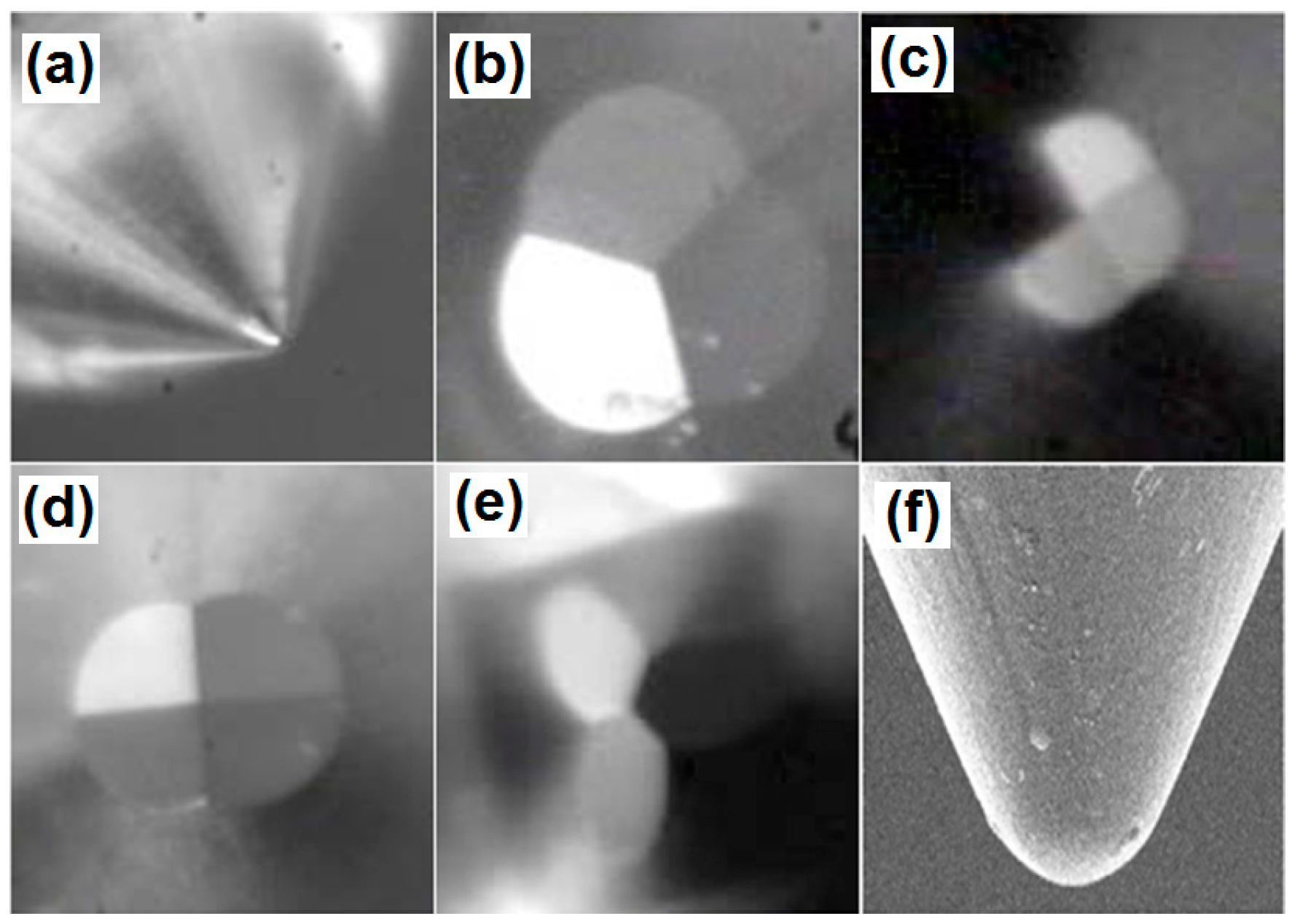
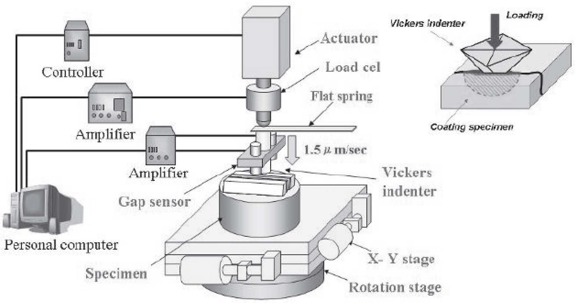
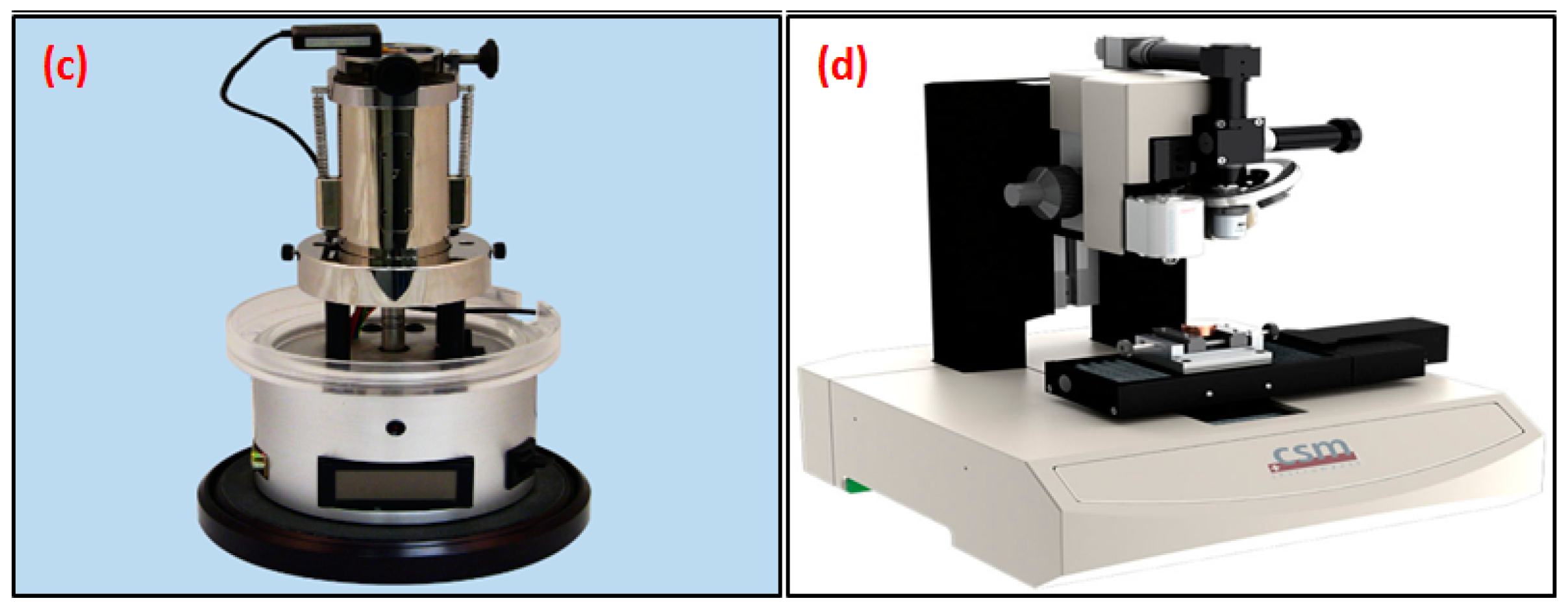
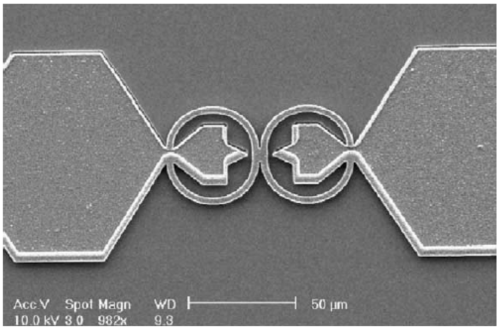
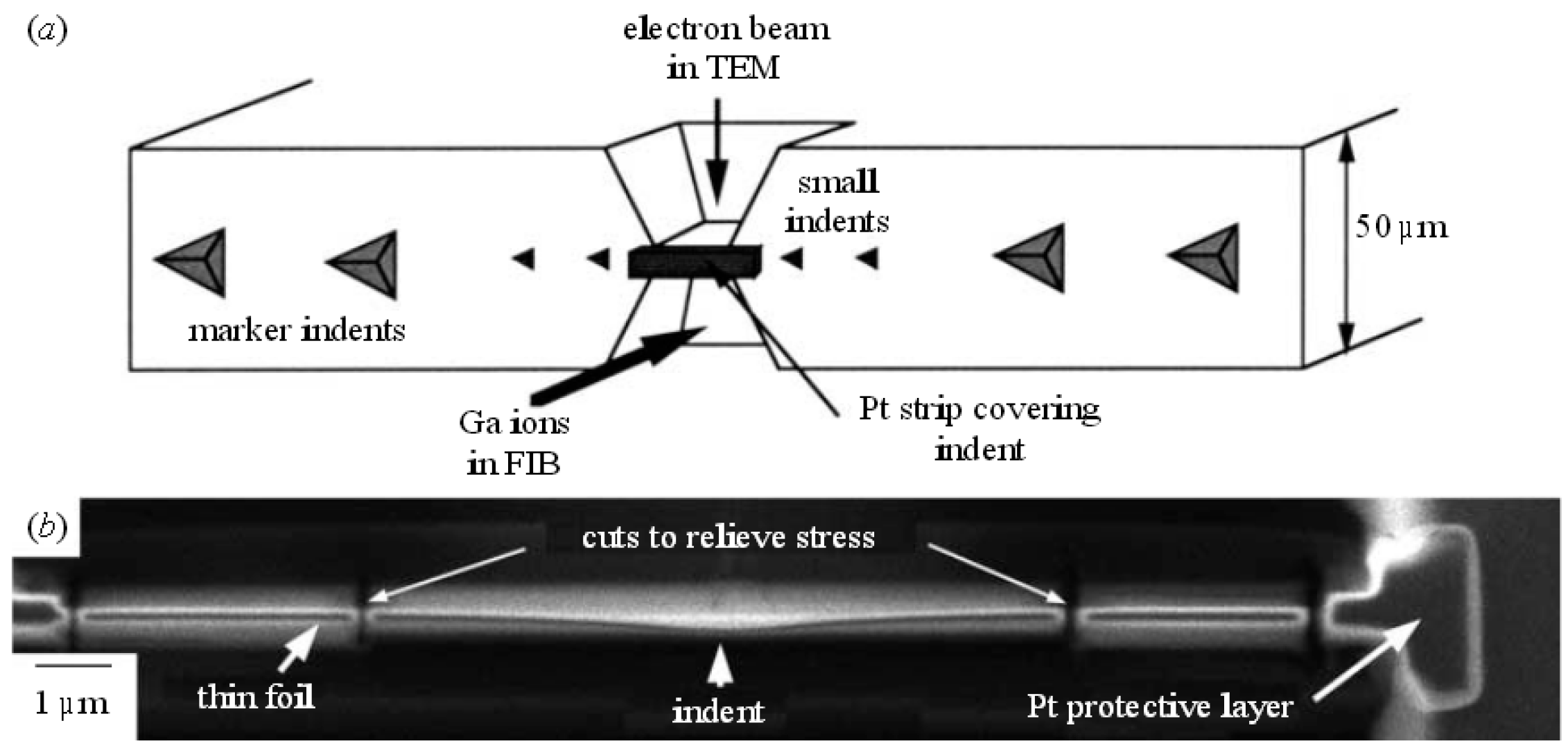
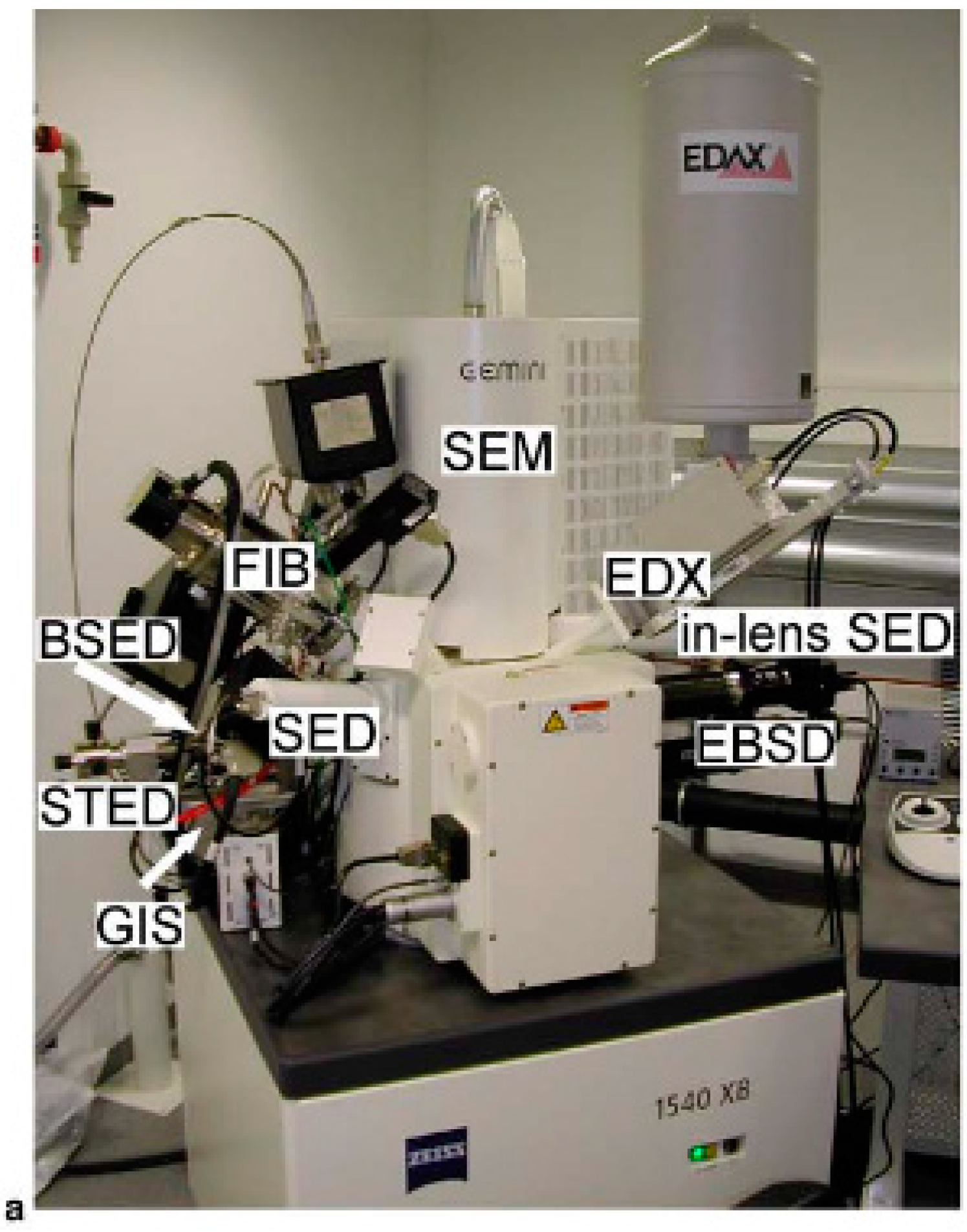
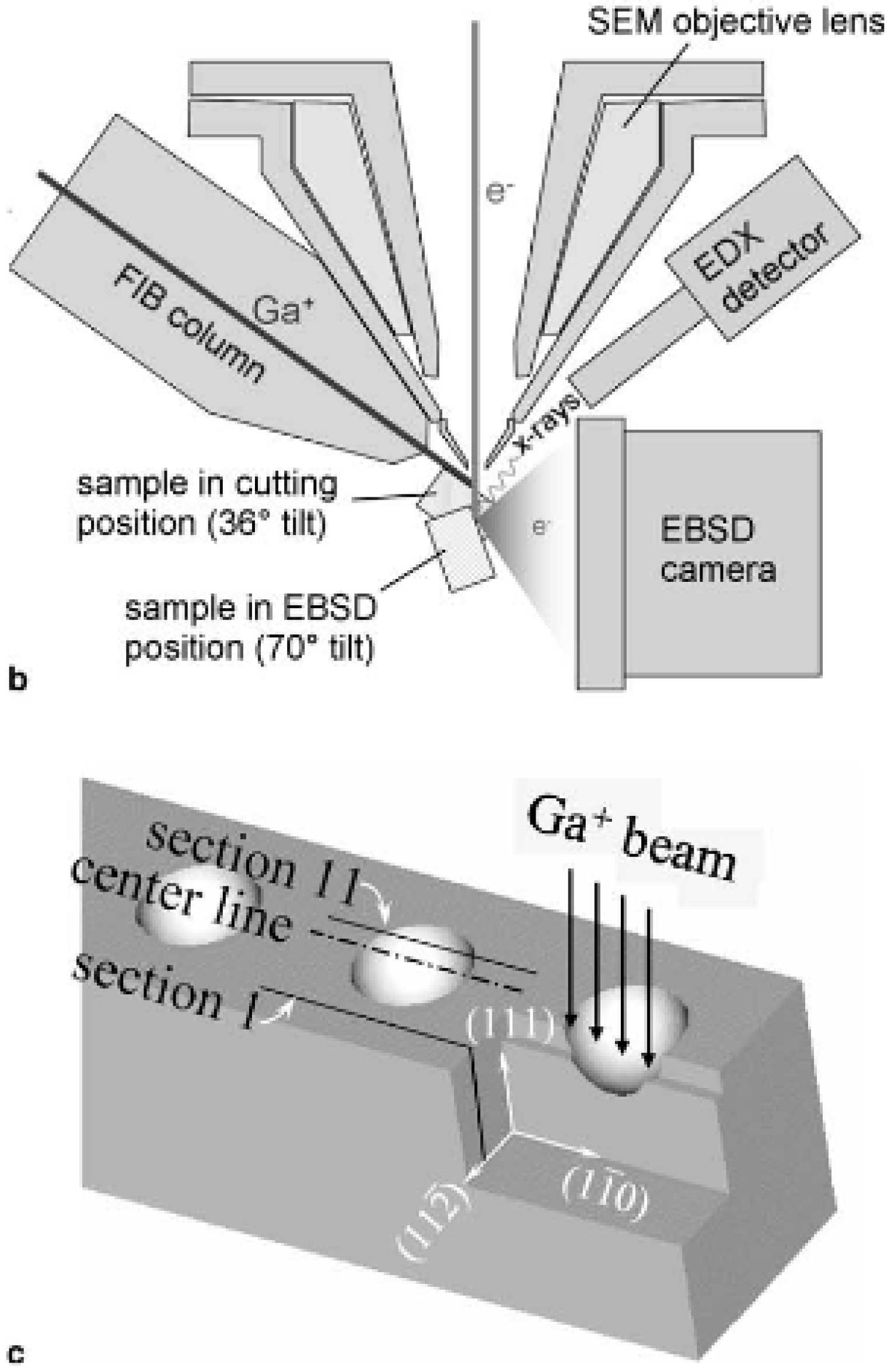
2. Nanoindentation Facilities

The most famous manufacturers of nanoindentation equipment include Keysight Technologies (Santa Rosa, CA, USA), Micro Materials Ltd. (Wrexham, UK), Fischer-Cripps Laboratories Pty Ltd. (Killarney Heights, Australia), Hysitron Inc. (Eden Prairie, MN, USA), and Anton Paar (Ashland, VA, USA). The iconic products of these manufacturers are shown in Figure 2. The working theories of different representative instruments are given in Figure 3. All of these instruments include three principal parts, namely indenter, load application, and capacitive sensor for measuring the displacements of the indenter. For instance, in Figure 3a, the load is applied by an electromagnetic coil which is connected to the indenter shaft by a series of leaf springs. The deflection of the springs is a measure of the load applied to the indenter, and the displacement usually can be measured by a capacitive sensor.
The indenter is conventionally made of diamond which has been ground to shape and sintered in a stainless steel chuck. The frequently used shapes of indenter are shown in Figure 4a–f [16]. The conical indenter has a sharp, self-similar geometry. Normally, the cone angle is either 60° or 90°, and the tip radii are 0.7, 1, 2, 5, 10, 20, 50, 100 and 200 μm [16]. The applications of conical indenter are extensive, including scratch testing, wear testing, nano-scale 3D imaging capturing and tensile, and compression tests on MEMS (Microelectromechanical systems). Berkovich indenter is the most frequently used indenter for indentation tests. The most noticeable feature of Berkovich indenter is that it is a three-sided pyramid which can be ground to a point, making it easy to maintain a self-similar geometry to micro-scale or nano-scale. The radius is about 150 nm when it is new and will become 250 nm 12 months later. The applications of Berkovich indenter are much more extensive, such as bulk materials tests, thin films tests, polymers tests, scratch testing, wear testing, MEMS tests and in situ imaging. The Vickers indenter is a four-sided pyramid and suitable for measuring mechanical properties on the very small scale, such as nano-scale as the line of conjunction at the tip limits the sharpness of tip for determination of hardness for very shallow indentation. The recommended applications include bulk materials tests, films and foils tests, scratch testing and wear testing.
The Knoop indenter is originally designed for hard metals. It is also can be used to probe anisotropy in sample surface. The Cube-corner indenter is a three-sided pyramid with mutually perpendicular faces, which is like the corner of a cube. The sharpness of the cube corner produces much higher stresses and strains in the area in contact with the indenter, thus makes it capable of producing very small and well-defined cracks around imprint in brittle materials. The toughness at microscale or nanoscale can be investigated via these induced fine cracks. Meanwhile, the Cube-corner indenter is fairly fragile and easily broken. The spherical indenter can be used to examine yielding and work hardening theoretically. Moreover, the elastic-plastic transition can also be investigated. The reason is, the contact stresses with spherical indenter are initially small and produce only elastic deformation, and with increasing indentation depth, a transition from elastic to plastic deformation can be captured. The parameters of all these indenters are listed in Table 1. Here, A denotes the projected area; R represents the contact radius of the indent pressed by spherical indenter; hp is the contact indentation depth; θ represents the semi angle of indenters; a is the effective cone angle and β denotes the geometry correction factor.

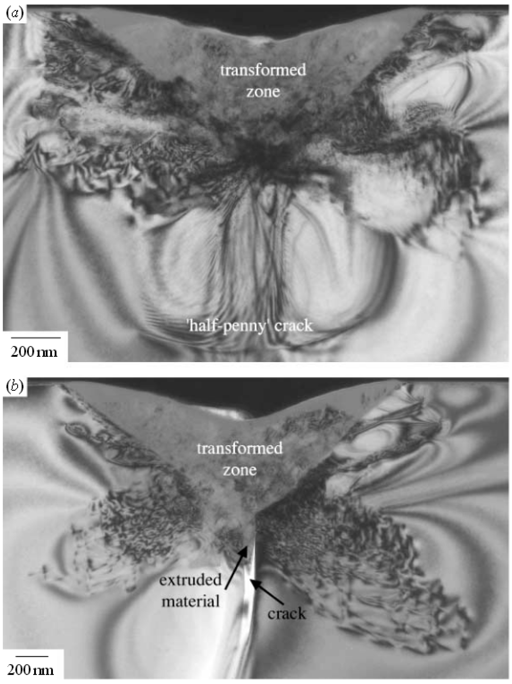
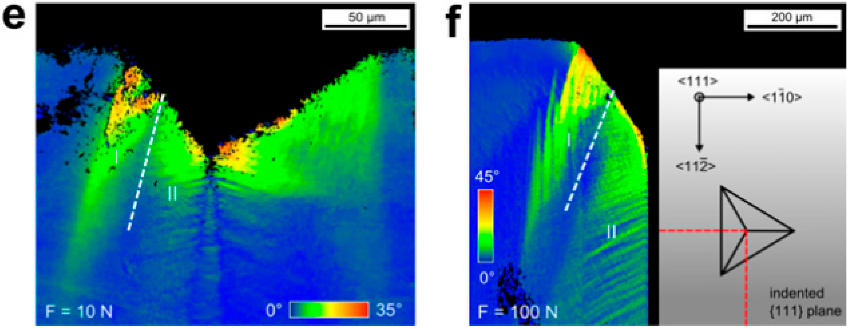
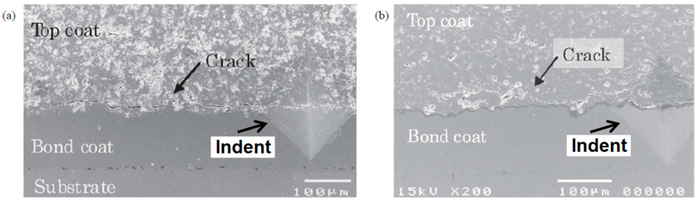
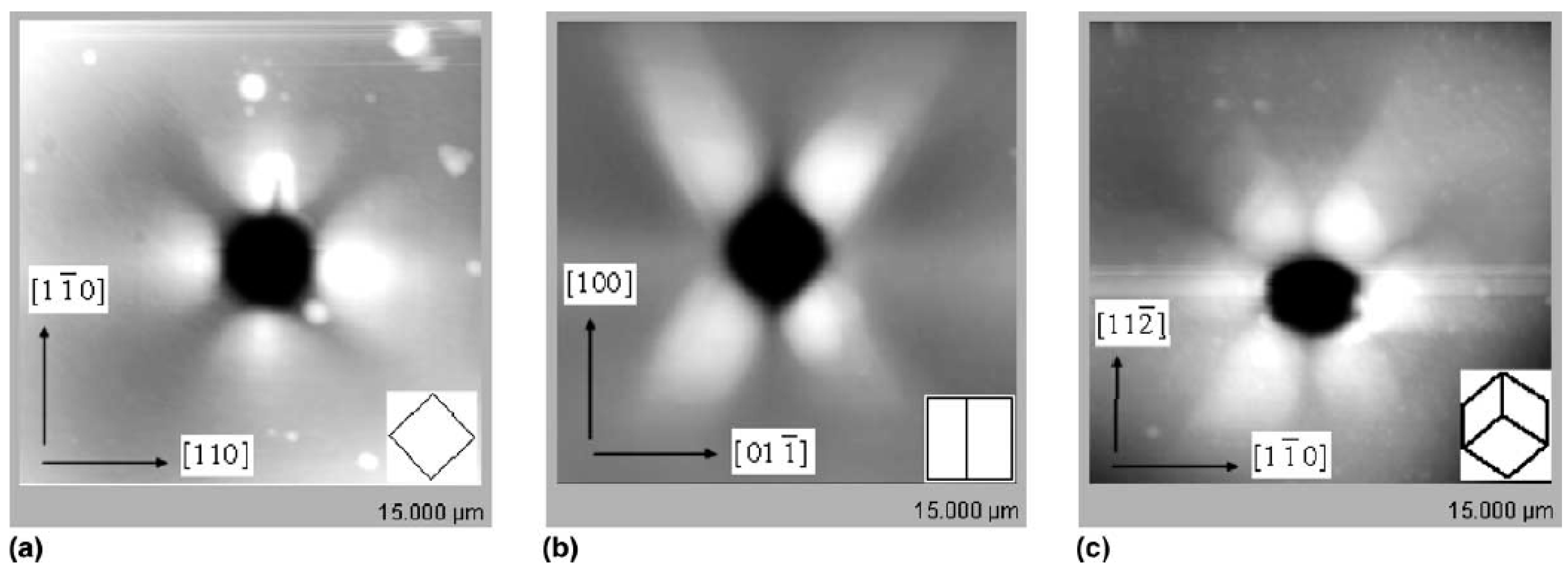
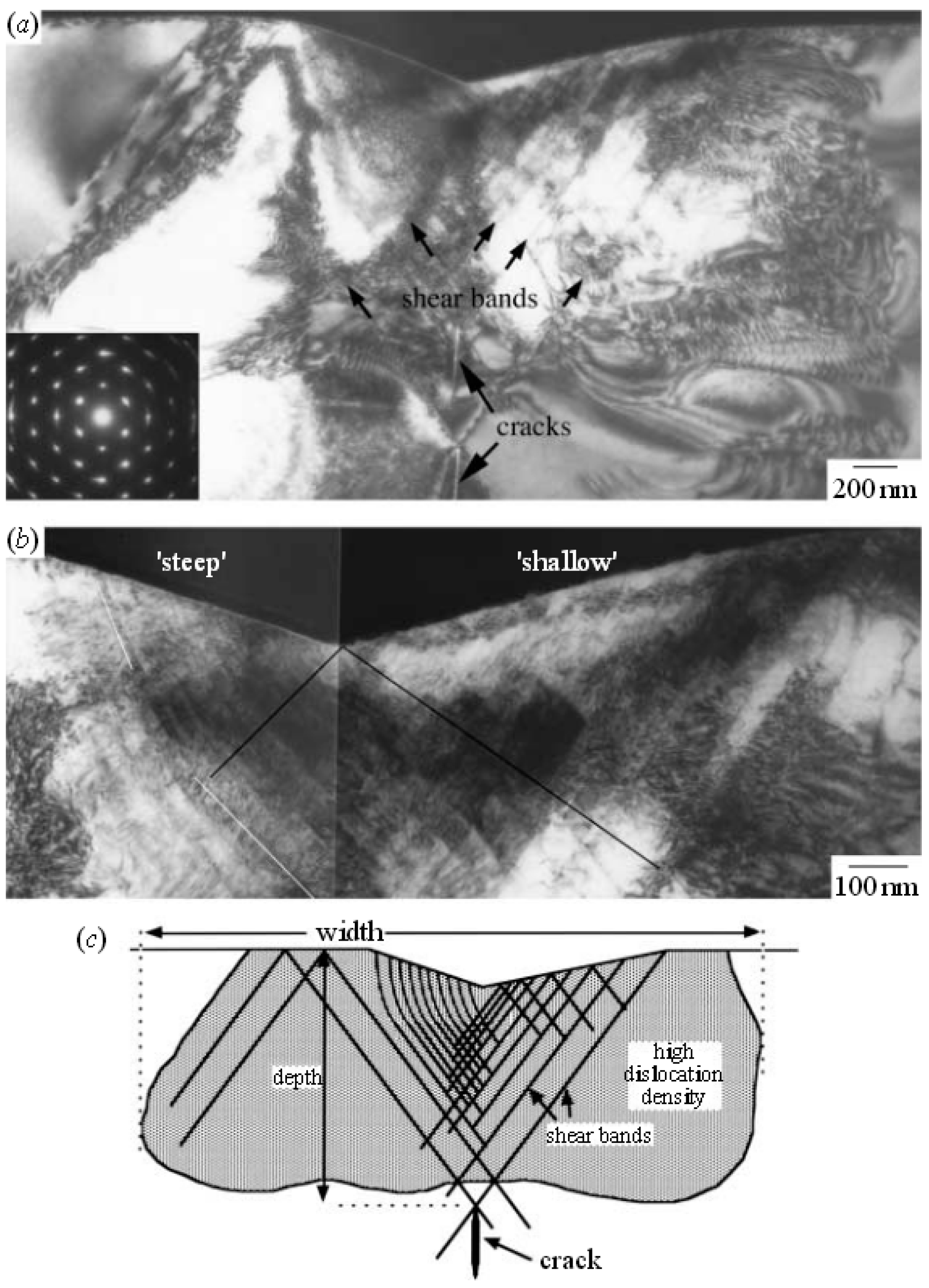
3. Application of Nanoindentation in Materials

In 1992, Oliver and Pharr [18] proposed a method to measure the Young’s modulus based on the indentation load-displacement curve, which was frequently used until now. Subsequently, they [19] provided a update of how to implement the method to make the most accurate measurents as well as the discussion of its limitations. Kucharski and Mroz [20] presented a new procedure for determining the plastic stress—strain curve by means of a cyclic spherical indentation test in 2007, which constitutes an ground-breaking improvement with respect to the traditional method. Kruzic et al. [21] improved the indentation techniques of evaluating the fracture toughness of biomaterials and hard human bones although accurately measuring the fracture toughness of brittle materials can be quite challenging. The fracture toughness can be obtained directly from indent crack length measurements, as shown in Figure 5.
Huber and Tsakmakis [22] proposed that nanoindentation tests can be used to identify effects of kinematic hardening on the material response. They also indicated that the identification may rely on the measurement of the opening of the hysteresis loop produced in the indentation load-displacement curve as shown in Figure 6. It is obvious that each material has a unique opening diagram indicating the corresponding effect of kinematic hardening.
Durban and Masri [23] in 2007 found that the nanoindentation test data with conical indenter over a range of cone angles can be used to reconstruct the axial stress-strain curve. Mata et al. [24] modified the previous hardness formulation within the elastic-plastic transition derived for solids by Hill [25] in 1950 and Marsh [26] in 1964 as it did not exhibit strain hardening.
Application of nanoindentation tests to determine the mechanical properties of surface coatings is another milestone. Normally, the investigations of the mechanical properties of the coatings are difficult as the traditional compression and tensile tests are unable to apply well at very small scales. Rodriguez et al. [27] performed depth sensing indentation in plasma sprayed Al2O3–13% TiO2 nano-coatings in order to determine the Young’s modulus and hardness. It was found the mechanical properties were dramatically enhanced in the nanostructured coating compared to the conventional one, which is shown in Figure 7. Swain, Menčík and their coworkers [28,29] investigated the application of five approximation functions (linear, exponential, reciprocal exponential, Gao’s, and the Doerner and Nix functions) for determining the Elastic modulus of thin homogeneous films. By conducting various experimental testes, they found that generally the Gao analytical function is able to predict the indentation response of film/substrate composites. For determining the thin film modulus from experimental data, satisfactory results can also be obtained with the exponential function, while linear function can only be used for thick films where the relative depths of penetration are small. For determing the hardness of thin films, Jönsson and Hogmark [30] built a physical model which was verified for chromium films on four different substrate materials.
Thin water film was studied by Opitz et al. [31] in 2003. It was believed that the thin water films which covered most of the micro-scale and nano-scale surfaces could be particularly important for microelectromechanical systems (MEMS) and the upcoming nanoelectromechanical systems (NEMS), as they played a critical role in defining the micro- and nano-tribological properties of a system. Kim et al. [32] presented a nanoindentation method to measure the Poisson’s ratio of thin films for MEMS applications. In their test, a double-ring-shaped sample was designed to conduct the measurement of the Poisson’s ratio as shown in Figure 8. The load-deflection data of the double ring sample after nano-indenter loading was analysed to obtain the Poisson’s ratio. Lou et al. [33] investigated the mechanical behaviour of LIGA (an acronym of the German words “lithographie, galvanoformung, abformung”) nickel MEMS structures which were developed for applications in micro-switches and accelerometers via the nanoindentaion method. Both Berkovich and Cube-corner indenter were used to conduct the nanoindentation tests and study the effects of residual indentation depth on the hardness of LIGA Ni MEMS structures between the mico-scale and nano-scales. Almost no apparent size dependence has been found for LIGA Ni films indented by a Berkovich indenter. In contrary, the hardness dramatically increased with decreasing residual indent depth for films indented by the Cube-corner indenter.
Indentation tests were also used to evaluate adhesion strength of the thermal barrier coatings (TBCs) which were used to improve the performance and efficiency of advanced gas turbines [34,35,36,37,38]. Interfacial strength was one of the most important properties in TBCs, and traditional tensile method was found to be restricted due to the size dependence. Yamazaki et al. [39] used the indentation method to investigate the interfacial strength of TBC which was subjected to thermal cycle fatigue. An indent was made directly at the interface on the polished surface of the sample as shown in Figure 9. The crack length and the diagonal length of the indentation were measured using SEM right after indentation as shown in Figure 10. The typical interfacial crack initiated by the indentation test in Figure 10a showed the crack mainly propagated in the ceramic top coat near the interface. Even after 500 thermal cycles with the formation and growth of TGO (thermally grown oxide) layer shown in Figure 10b, the crack propagated only in the ceramic top coat too.
The dependence of nanoindentation piling-up patterns and of micro-textures on the crystallographic orientation was studied by Wang et al. [40] using high purity copper single crystal with three different initial orientations. The indentation tests were performed on a Hysitron nanoindentation setup using a conical indenter to avoid symmetries. The results are shown in Figure 11. Four-, two-, and sixfold symmetrical piling-up patterns were captured on the surface of (001), (011) and (111) initial oriented single crystal, individually, which could be explained in terms of the strong crystallographic anisotropy of the out-of-plane displacements around the indenter.
With the development of focused ion beam milling of site-specific electron transparent foils, the investigation of cross-sections of nanoindentations with the transmission electron microscope (TEM) or electron backscatter diffraction has recently become feasible [41]. Lloyd [42] and his colleagues combined nanoindentation and TEM to survey the deformation behaviour in a range of single crystal materials with different resistances to dislocation flow as shown in Figure 12. The principal deformation models included phase transformation (silicon and germanium), twinning (gallium arsenide and germanium at 400 °C), lattice rotations (spinel), shear (spinel), lattice rotations (copper) and lattice rotations and densification (TiN/NbN multilayers). Generally, the residual impresses were sectioned through the tip of the indent with the thin foil normal approximately parallel to either [110] or [100] zone axis.
The indents in (001) silicon at loads of 30 mN and 60 mN are shown in Figure 13. It was found a transformed region was under the area of the Berkovich indenter in both cases, and a crack was originating at the base of the transformed region in the case of 60 mN.
Shear bands were captured in spinel crystals, which are shown in Figure 14 and Figure 15. It was found the shear band spacing increased with increasing distance from the indent tip, and the spacing on the steep side of the indent was a little smaller for the large load. Lloyd [43] concluded that the increase of the shear band spacing with distance far away from the indenter tip indicated there was a limit to the amount of displacement occurring through any shear band due to strain hardening. Consequently, a high concentration of shear bands was close to the indenter tip where had the largest vertical displacements, while a low density of slip bands was sufficient to accommodate the relatively small vertical displacement in the region far away from the indenter tip.
Lattice rotation angles around an axis perpendicular to the [110] zone axis were investigated [42] and are shown in Figure 16. It was found the rotations only occurred in the region immediately below the indent impression. The greatest rotations were quite near the indent tip and the magnitude of rotation angles decreased significantly with the increasing distance from the indent tip along the surface on the shallow side.
The indentation-induced plastic zones below indentations in copper single crystals, with depths ranging from 250 nm to 250 μm, were examined by Rester et al. [44] via the implementation of focussed ion beam (FIB) and electron backscatter diffraction (EBSD) techniques. Two or three distinguishable regimes shown in Figure 17 were captured by analysing scanned orientation micrographs. Meanwhile, the changes in the evolution of the microstructure were reflected in the hardness curve shown in Figure 18. Regime α described the impression which is smaller than 300 nm, in which no significant orientation changes are observed by EBSD (Figure 17a). Regime β describes the indentation depth between 300 nm and 30 μm, which is characterized by regions having noticeable changes of the orientation (Figure 17c,d). It was also found that the orientation differences increase with growing indentation depth in this regime. Regime γ is associated with indentation depth larger than 30 μm exhibiting a typical substructure of FCC (face centered cubic) single crystal of pure metals during indentation. Therefore, Rester et al. [44] concluded that the hardness of a material varies with the size of the indent impression and the source size becomes the dominant effect only for very small impressions (i.e., in regime α).
Zaafarani et al. [45] investigated texture and microstructure below a conical nano-indent in a (111) oriented Cu single crystal using 3D EBSD. The tests were performed using a joint high-resolution field emission scanning electron microscopy/electron backscatter diffraction (EBSD) set-up coupled with serial sectioning in a focused ion beam system in the form of a cross-beam 3D crystal orientation microscope (3D EBSD) as shown in Figure 19.
The EBSD tests conducted in sets of subsequent ( 11 2 ¯ ) cross-section planes exhibited a pronounced deformation-induced 3D patterning of the lattice rotations below and around the indent, which are shown in Figure 20.

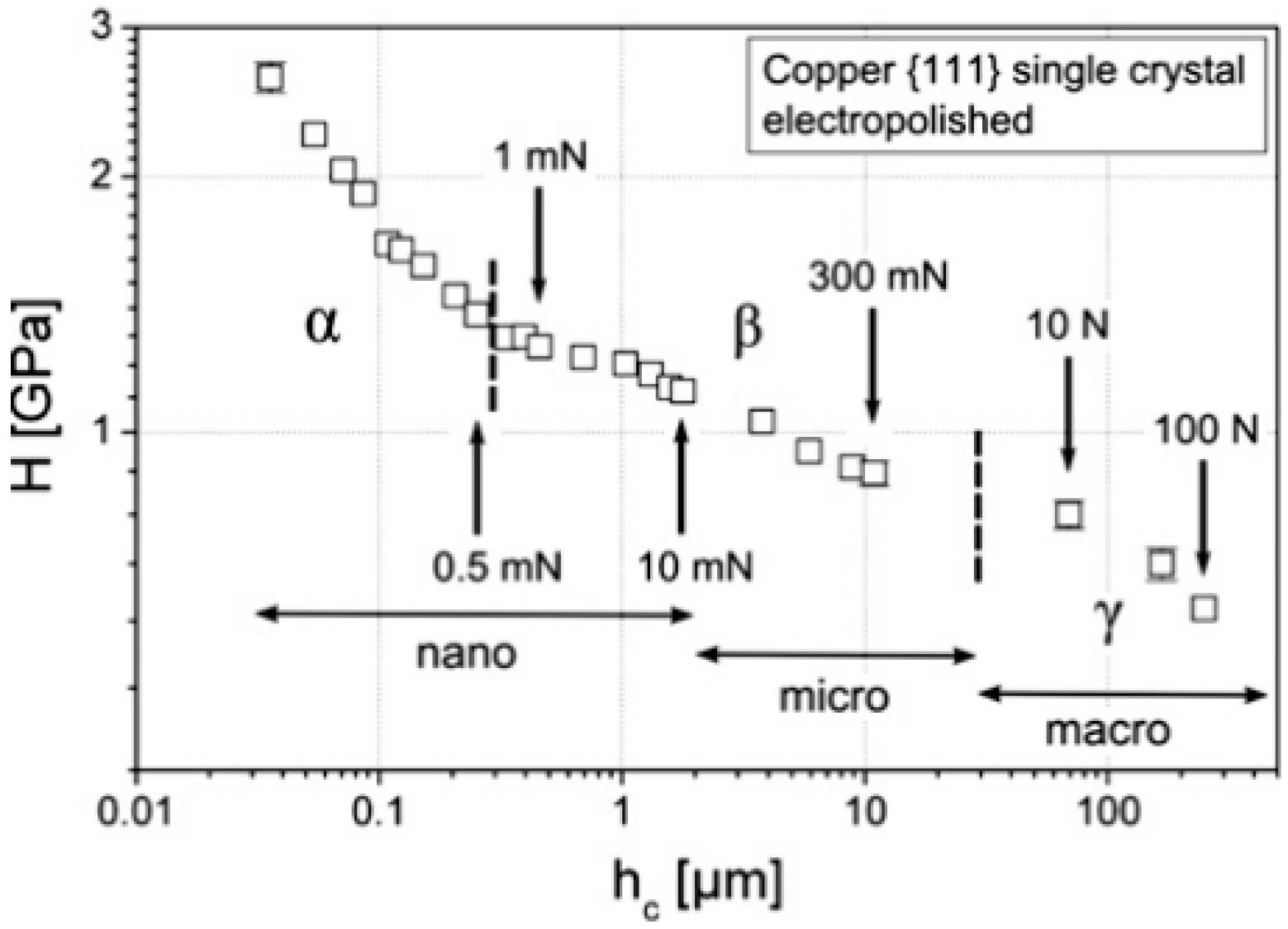
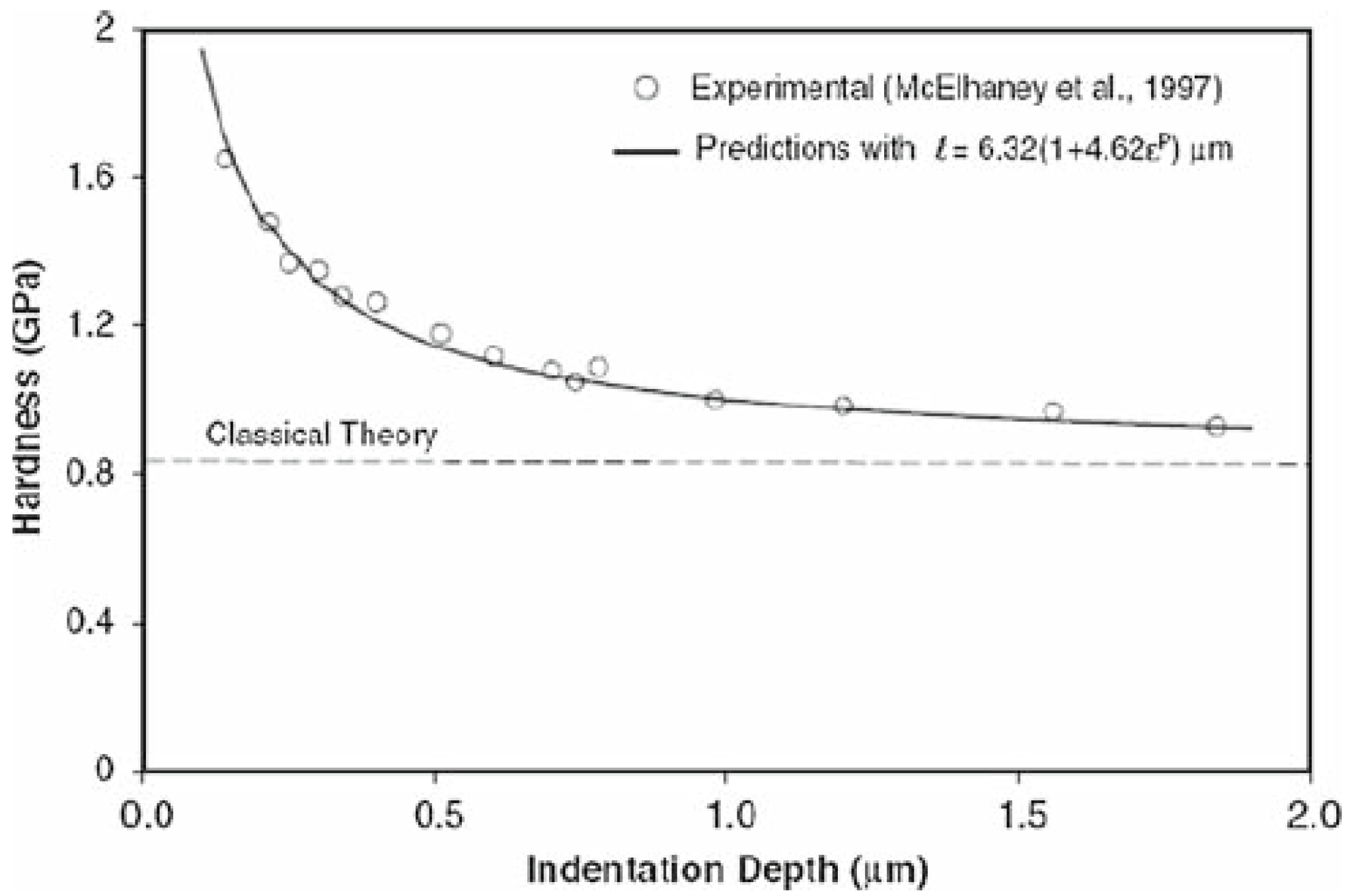
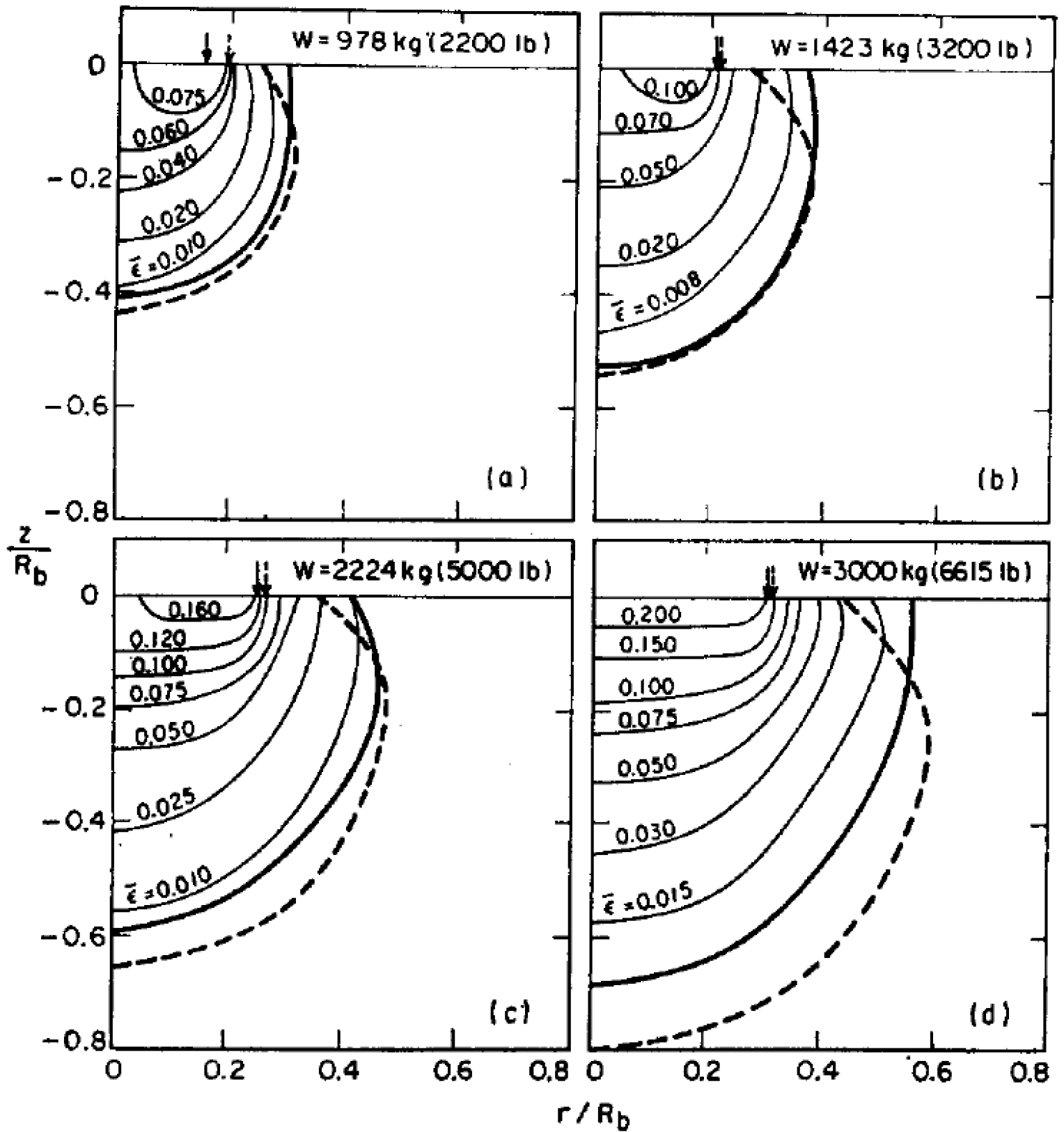
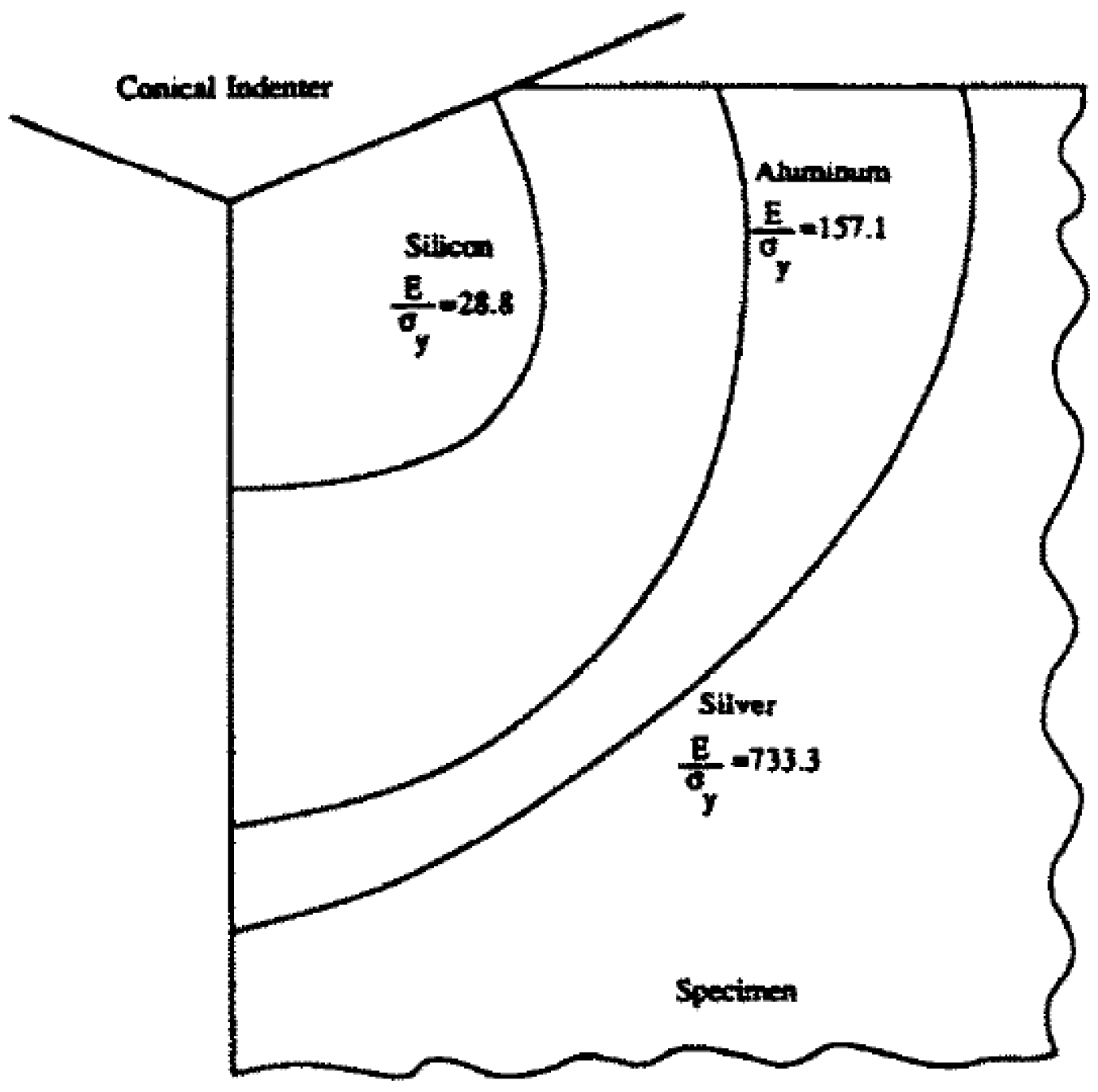
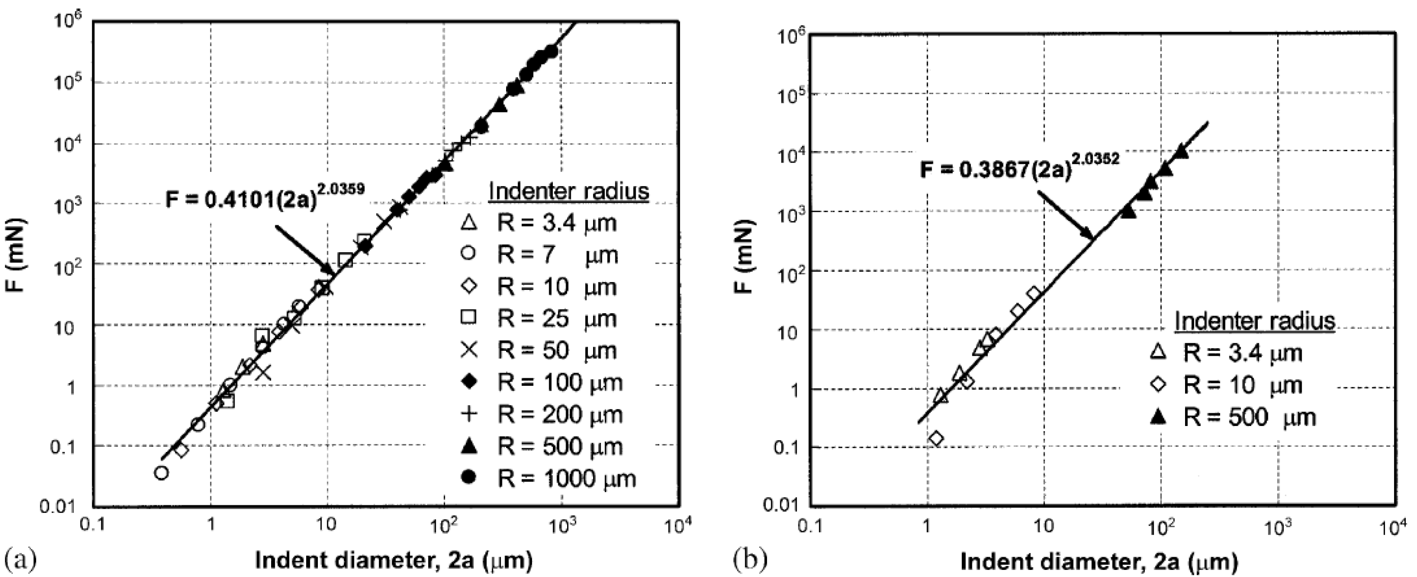
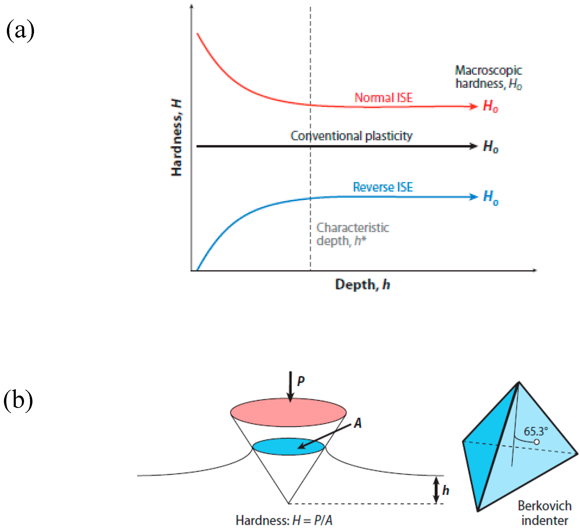
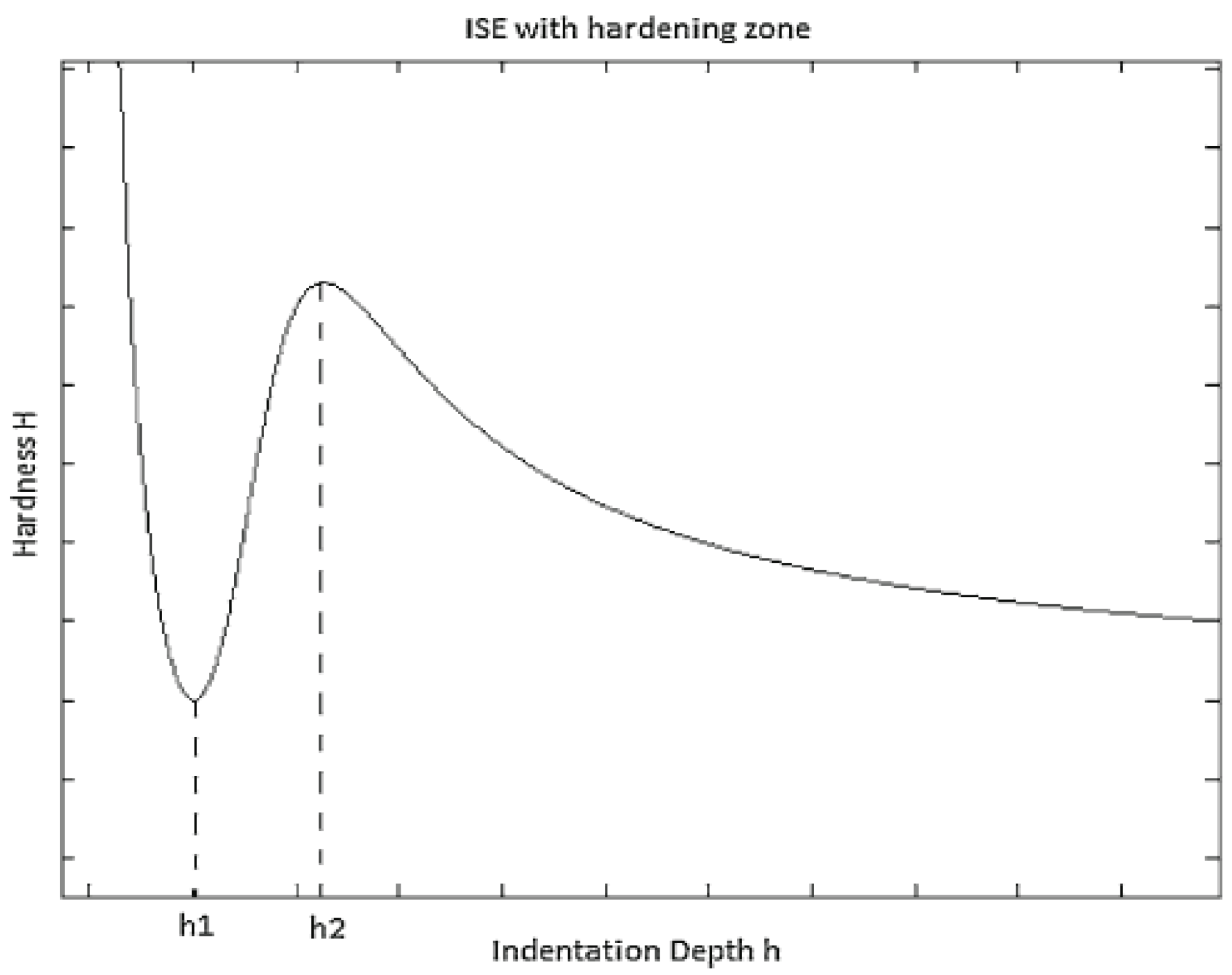
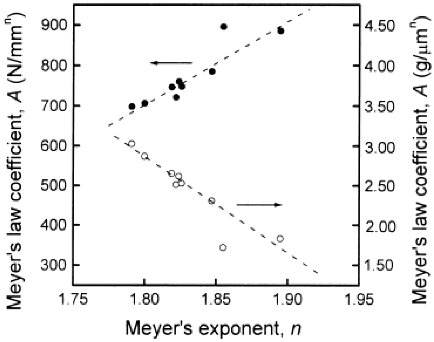
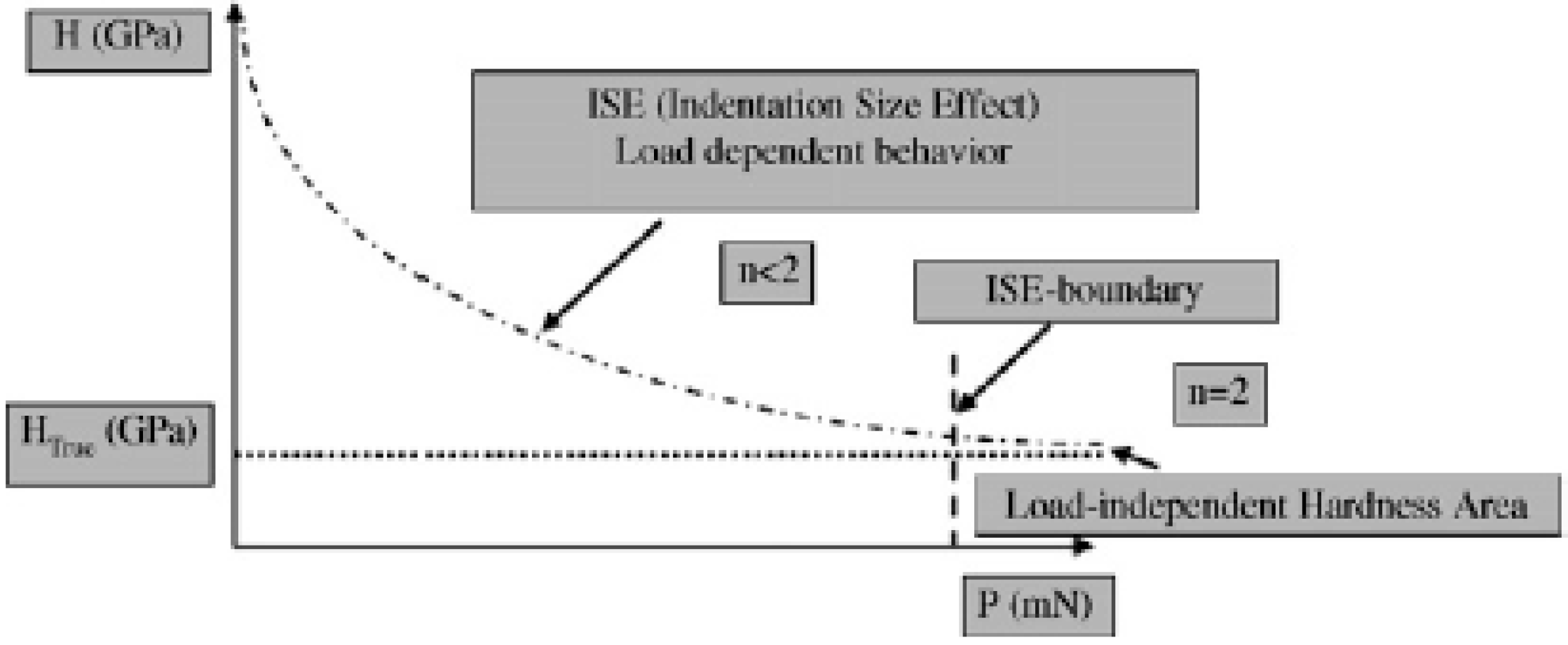
4. Nanoindentation Size Effect of Materials

Over the past several decades, with the development of new technologies, people felt that it was very important to understand how materials perform at small scales because the mechanical properties are significantly different from those at macro-scales. Therefore, a great number of researchers became interested in micro- and nano-scale deformation phenomena which also made them try to look for a new method to examine these physical phenomena at ever-decreasing length scales. In the field of the mechanical behaviour of materials, one of the more interesting small-scale phenomena is an increase in yield or flow strength that is often observed when the size of the test sample is reduced to micro-meter and sub-micrometer dimensions [46]. Pharr et al. [46] believed such size-dependent increases in strength were due to unique deformation phenomena which could be observed only when the sample dimensions approached the average dislocation spacing and when plastic deformation was controlled by a limited number of defects.
In the metal micro-forming process, grain size, grain orientation and material’s dimension are the important influence factors for the material’s deformation. It is reported that when the dimension of the material is downscaled to a much smaller scale, the mechanical properties are significantly different from those on the macro-scale, which is called ‘size effect’ [47]. Size effect is an interesting and important topic for the development of micro-forming technologies. Recently, numerous experiments have shown that metallic materials display noticeable size effects once the size of non-uniform plastic deformation zone associated their characteristic length size are on the order of microns [47]. Fleck et al. [48] found a dramatic increase of plastic work hardening when the wire’s diameter decreased from 170 μm to 12 μm via doing thin copper wire’s torsion experiments. Stolken and Evans [49] observed that the plastic work hardening increased significantly when the nickel beam thickness was decreased from 50 μm to 12.5 μm while doing a micro-bend test. Gau et al. [50] found that the conventional concept of spring-back cannot be applied on brass sheet metal when its thickness is less than 350 μm by studying the spring-back behaviour of brass in micro-sheet forming. Geiger et al. [51] and Kals and Eckstein [52] have conducted compression tests, tension tests, and bending tests, respectively, in order to study how the material properties change due to size effect. Saotome et al. [53] carried out investigations in micro-deep drawing, and found that the relative punch diameter (punch diameter related to the sheet thickness) has a significant influence on the limit draw ratios (LDR).
The indentation size effect (ISE) is often observed for materials that are indented with geometrically self-similar indenters like pyramidal or conical tips (see Figure 21) [46]. In general, the hardness, H, defined as the load on the indenter normalized with the projected contact area of the hardness impression (see Figure 21), should be independent of the depth of penetration, h. However, over the past 60 years, it was observed that there were significant variations of hardness with respect to penetration depth, especially when the depths decreased to less than a few micro-meters [54,55,56,57,58,59,60]. In addition, two types of indentation size effects have been reported. One is the normal ISE (the tip is pyramidal or conical)—the hardness increases with decreasing penetration depths, according to the expression “smaller is stronger” (see Figure 21). Another one is the reverse ISE (the tip is spherical) [55,56,61], which displayed that the hardness decreases with increasing depths. However, for the reverse ISE, it was observed that the hardness also increases with the decreasing of tip radius. The reverse ISE is thought to be derived from testing artefacts such as vibration in the testing system or problems with accurate imaging and measuring the sizes of hardness impressions at dimensions approaching the limits of optical microscopy [46].
Although classical descriptions of the ISE show a decrease in hardness for increasing indentation depth (Figure 22), recently new experiments [62] have shown that after the initial decrease, hardness increases with increasing indentation depth. After this increase, eventually the hardness decreases with increasing indentation (Figure 23). This phenomenon is very prominent for copper, but not noticeable for aluminium.
There are different theories to explain ISE. The most popular theory is based on strain gradient plasticity which is a class of continuum theories aimed to bridge the gap between classical plasticity and dislocation. This theory assumes that the flow stress of metals depend on the density of statistically stored dislocations (SSD) which relate to effective strain, and the density of the geometrically necessary dislocations (GND) which relate to the strain gradient. Dislocations are generated, moved and stored during the process of plastic deformation. The process of storing dislocation is also a process of strain hardening. It is assumed that dislocations become stored because they either accumulate by randomly trapping each other or they are required for compatible deformation of various parts of the material. When they randomly trap each other, they are often known as the statistically stored dislocation [63], whereas when they are required for the compatibility purpose, they are often called geometrically necessary dislocations and related to the gradient of plastic shear strain in a material [63,64].
The most famous strain gradient plasticity model for nanoindentation was proposed by Nix and Gao [65] in 1998. It has been assumed that plastic deformation of the surface is accompanied by the generation of dislocation loops below the surface, which are contained in an approximately hemispherical volume below the region in contact, as shown schematically in Figure 24. The deformation is self-similar and the angle (θ) between the conical indentation tip and indented surface remains constant.
The angle θ can be calculated by
  t a n ( θ ) = h a = b G L G ,   L G = b G a h
where h is the residual plastic depth, and a is the contact radius, and bG is Burger’s vector. The number of geometrically necessary dislocation loops is h/bG. S is the spacing between individual slip steps on the indentation surface, as shown in Figure 24. Assume that λ is the total length of the injected loops, thus between r and r + dr we have
d   λ = 2 π r d r S = 2 π r h b a d r
which after integration from 0 to a gives the total length of dislocation loops,
λ = 0 a h b a 2 π r d r = π h a b
The model assumes that the dislocations are distributed uniformly in a hemispherical volume with the contact radius.Thus, we have V = 2 π a 3 / 3 , and therefore the density of geometrically necessary dislocation is
ρ G = λ V = 3 2 b h t a n 2 θ
Taylor hardening model has been used to find the shear strength which can be used to measure the deformation resistance:
τ = α µ b ρ T = α µ b ρ G + ρ S
where τ is the resolved shear stress, μ is the shear modulus, b is the Burgers vector and α is a constant which is usually in the range 0.3–0.6 for FCC metals [66]. Here, they note that ρ S does not depend on the depth of indentation. Rather it depends on the average strain in the indentation, which is related to the shape of the indenter (tan(θ)). They also assume that the von Mises flow rule applies and that Tabor’ factor of 3 can be used to convert the equivalent flow stress to hardness:
σ = 3 τ , H = 3 σ
According to these relations the hardness can be expressed by as:
H H 0 = 1 + h * h
where
H 0 = 3 3   α µ b ρ S
is the macroscopic hardness from the statistically stored dislocations alone, in the absence of any geometrically necessary dislocations, and
h * = 81 2 b α 2 t a n 2 θ ( μ H 0 ) 2
is a length scale for the depth dependence of hardness.
From Equation (12), it can be seen that the indentation hardness H is related only to indentation depth h as h * and H 0 are material constants which can be obtained by fitting the experimental results.
After Nix and Gao [67], many other researchers continue to observe ISE through experiments and simulations. Most of them explained the size effect via the strain gradient theory (Ma and Clarke [68], Fleck et al. [48], Nix and Gao [65], Poole et al. [69], Stelmashenko et al. [70], Gao et al. [71,72], Acharya and Bassani [73], Huang et al. [74], and Gurtin [75]). They believed that ISE must have a relationship with the strain gradient as the geometrically necessary dislocation density   ρ G is usually related to an effective strain gradient η as
ρ G = 2 η b
According to Equation (9), strain gradient was inversely proportional to the indentation depth h, which meant strain gradient should be larger at the shallow depth.
However, Demir, Raabe and Zaafarani [76] expressed a different theory about ISE. They thought as ρ G is the GND density that is required to accommodate a curvature   ω , the crystallographic misorientation between two neighboring points can be used as an approximate measure for the GNDs as shown in the following equation:
ρ G = ω b
According to Equations (15) and (16), the size dependence of indentation hardness has been associated with strain gradients which exist in the lattice through GNDs. Thus, these researchers decided to directly measure lattice rotations below indents with the aim of quantifying the density of these defects. For this purpose they performed an experiment using a tomographic high-resolution electron backscatter diffraction orientation microscope in conjunction with a focused ion beam instrument to map the orientation distribution below four nanoindents of different depths. Unfortunately, the experimental result contradicted the commonly expected inverse relationship between the indentation depth and the density of the GNDs. In terms of GND-based strain gradient theories, larger GND densities should appear at shallow indentation depth, not at a deep one. But their experiment showed an opposite trend that the total GND density below the indents reduces with decreasing indentation depth. According to the experimental results, they concluded that the explanation size-dependent material strengthening effects by using average density measure for GNDs was not sufficient to understand the indentation size effect.
Kiener [57] investigated Nix-Gao model with the cross-sectional EBSD method and proposed that Nix-Gao model’s physical basis was still under debate, and its validity cannot be addressed alone with load versus displacement characteristics. There were two assumptions with respect to the Nix-Gao model, hemispherical plastic zone and self-similarity of the evolving deformation structure. However, according to the EBSD observation shown in Figure 17, it is clear that the true plastic deformed zone deviates from the assumption of a half-sphere. Other reports indicated that there were differently shaped deformation areas, depending on the indenter geometry [45,77,78]. Regarding the self-similarity, based on the Nix-Gao model, the strain gradient induced by the indenter should be determined solely by the indenter geometry. Therefore, it should be constant for self-similar indenter shapes, which means the observed misorientations should depend only on the indenter angle and not on the indent size. However, the observations for Vickers indents in copper and tungsten displayed that the maximum misorientation was along the indent flanks for different sizes, as shown in Figure 25.
Furthermore, Nix-Gao model assumed that GNDs would accommodate the impression geometry at very low indentation depth for metallic materials with no pre-existing defects, such as single-crystal metals without any deformation. Subsequently, it was generally accepted that ISE would not exist in materials with pre-existing high dislocation densities, such as ultrafine-grained materials [79] and amorphous materials. However, recently Smedskjare [80] and Liu et al. [81] found ISE existing in oxide glasses and photonic crystals, respectively. Obviously, all of these materials are not crystalline metallic materials. Therefore, it is concluded that ISE may commonly exist in natural materials, not only in crystalline materials.
Meyer’s law is another widely used method to describe ISE. For the indenters which have ideal geometry, the relationship between the test load and the resultant indentation diagonal length curve could be obtained from [67]
P = C · d n
where P is the load, d is the diagonal length of impression, C is the material/indenter constant and n is the Meyer index due to the curvature of the curve. Since d is proportional to the contact depth h c which in turn is proportional to the indentation depth h, Equation (17) could be expressed as follows:
P =   C · h n
where C is constant and h is the indentation depth.
Fischer-Cripps [84] mentioned that if the plastic zone was fully developed (beyond elastic-plastic transition point), the load-displacement (P-h) curve of the loading section could be related to the square of the displacement ( P =   C h 2 ). As for the loading stage of the P-h curve in the elastic-plastic field. Sakai [85] stated that the load is proportional to the square of the indentation depth. According to Equatoion (17), if n = 2, the materials shows no ISE. But if n < 2, the materials shows ISE and this case was confirmed by different materials [86,87].
Considering aforementioned facts, Ebisu and Horibe [67] analyzed the relationship between the P-h curve and ISE behaviour in their experiments by differentiating the P-h curves of the three samples. They found that for single 8Y-FSZ (8 mol %Y2O3–ZrO2 single crystal) in the load range of 200–1900 mN, the index n calculated from the P-h curve was 1.873, which suggests that single 8Y-FSZ showed ISE behaviour. They also found this ISE result agreed well with the experimental results of another report [88] in which the hardness decreased as the indentation increased between the load range of 100–2000 mN. The same procedure was conducted in the 12Ce-TZP P-h curve and they found n = 1.808 within the load range 200–1900 mN. It also was consistent with the results (ISE behaviour) from zirconia ceramics [88,89]. However, for fused quartz, index n = 1.961 calculated from P-h curve in the load range of 200–1900 mN meant that this material showed almost no ISE behaviour [67]. This agreed with Oliver and Pharr’s report [18] which stated that quartz showed very little indentation size effect.
Kolemen [90] conducted the same experiments with superconductors, which showed a apparent ISE. He then concluded that for hard materials like brittle ceramics at low indentation loads, n is significantly less than 2. According to Onitsch [82], n lied between 1 and 1.6 for hard materials and higher than 1.6 for soft materials.
However, Peng et al. [91] pointed out the correlation between n and C seemed to be of little significance for understanding the ISE, as their previous study has showed that the best-fit value of the Meyer’s law coefficient C depended on the unit system used for recording the experimental data and completely different trends of n versus C may be observed in different unit systems [92] as shown in Figure 26.
The first unit system used is P in Newton (N) and d in millimeter (mm) and the second is P in gram (g) and d in micrometer (mm). As can be seen from Figure 26, completely different trends of n versus A were observed in different unit systems. Similar conclusions were reported by Li and Bradt [93] when they analyzed the experimental data on single crystals. Therefore, they concluded that a particular care should be taken when analyzing the microstructural effects on the measured hardness based on Meyer’s power law.
It should be noted that only n plays an important role in determining ISE in Meyer’s law and it is not necessary to consider the variation of Meyer’s law coefficient C. Although numerous researchers used Meyer’s law to analyse ISE, all of them just fit the whole P-h curve. In fact, the P-h curve can be fitted separately from the ISE-boundary which is shown as in Figure 27. In the left side of ISE-boundary an n-value smaller than 2 can be obtained, while an n-value of about 2 can be achieved in the right side.
Some other factors may influence the ISE, which include: inadequate measurement capabilities of extremely small indents [94], presence of oxides or chemical contamination on the surface [95], indenter-sample friction [96], and increased dominance of edge effects with shallow indents [68].
Elmustafa and Stone [97] proposed a vast number of hypotheses to explain the ISE, including: friction, and lack of measurement capabilities, and surface layers, oxides, chemical contamination and dislocation mechanisms. To calculate the hardness for the nanoindentation measurements, indents were imaged in calibrated optical and scanning electron microscopes. However, because of the inaccuracies inherent to “optical” method, they did not just rely on them alone. In addition, they used contact stiffness as a method to determine indirectly the projected contact area. Interestingly, the two methods agreed very well.
Elmustafa et al. [97] conducted experiments using alpha brass and aluminium as samples. It has been found that the oxide on a fresh surface of alpha brass is less than 5 nm thick, while the oxide thickness on an aluminium surface is only 1–3 nm [98]. For Elmustafa et al.’s experiment, the smallest indents were approximately 0.3 um across or 60 times larger in lateral dimensions than the oxide thickness. Therefore, the oxide layer would not greatly affect the hardness.
The indenter piling-up or sinking-in was also seen as a factor that influences ISE. McElhaney et al. [99] did numerous experiments and found that the indenter piling up and sinking in had a huge effect on the micro-indentation hardness. However, after very careful examination, they found the indentation hardness still displayed strong dependence on the penetration depth. This observation displayed that the indenter piling up and sinking in cannot explain the depth-dependent indentation hardness alone.
Loading rate was raised as another influence factor for ISE because usually materials tended to display larger a plastic work hardening at a large strain rate (loading rate) [100]. The strain rate in the indented material should be proportional to the ratio h ˙ h , where h ˙ is the rate of change of the indentation depth and h is the indentation depth. It is not hard to understand that for a constant rate of indentation depth ( h ˙ = c o n s t a n t ) , the strain rate should be very huge at the initial penetration. However, Lilleodden [101] performed indentation test at a constant ratio h ˙ h and still observed the phenomenon of ISE.
Indenter tip radius was regarded as another factor which affected ISE. However, McElhaney et al. [99] and Huang et al. [102] found that the sharp indenter tip radius less than 100 nm had definitely no influence on the micron and sub-micron scale indentation, which indicated that indenter tip radius cannot be used to explain the ISE observed in the indentation test with sharp indenters.

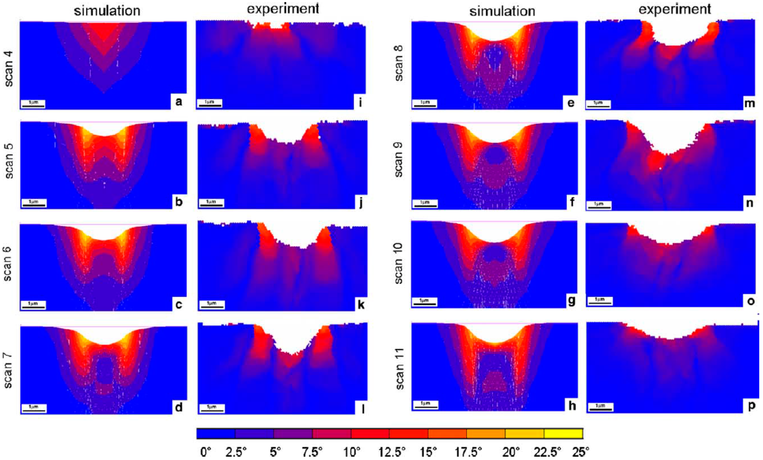
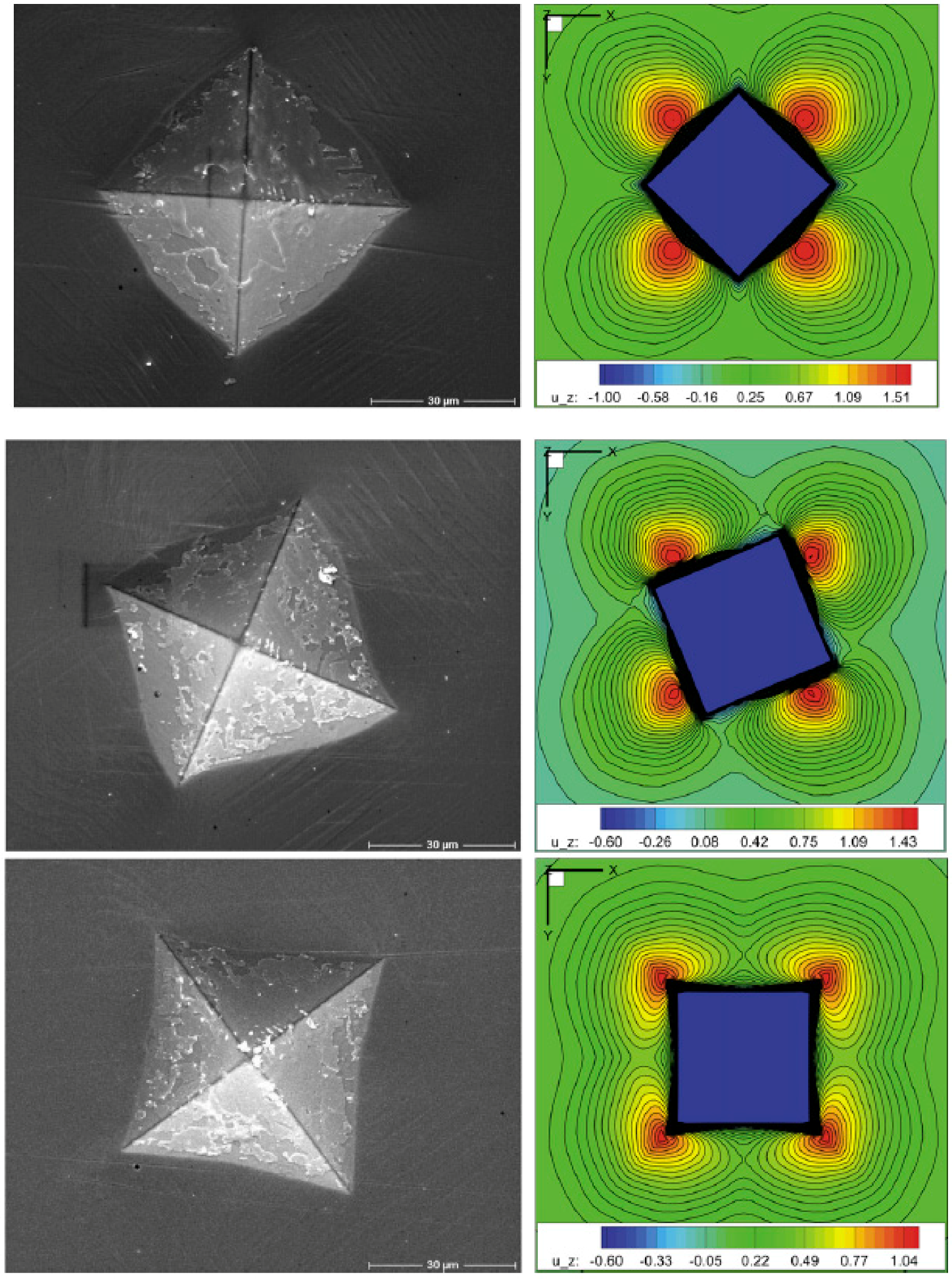
5. Simulations of Mechanical Behaviours of Materials Undergoing Nanoindentation

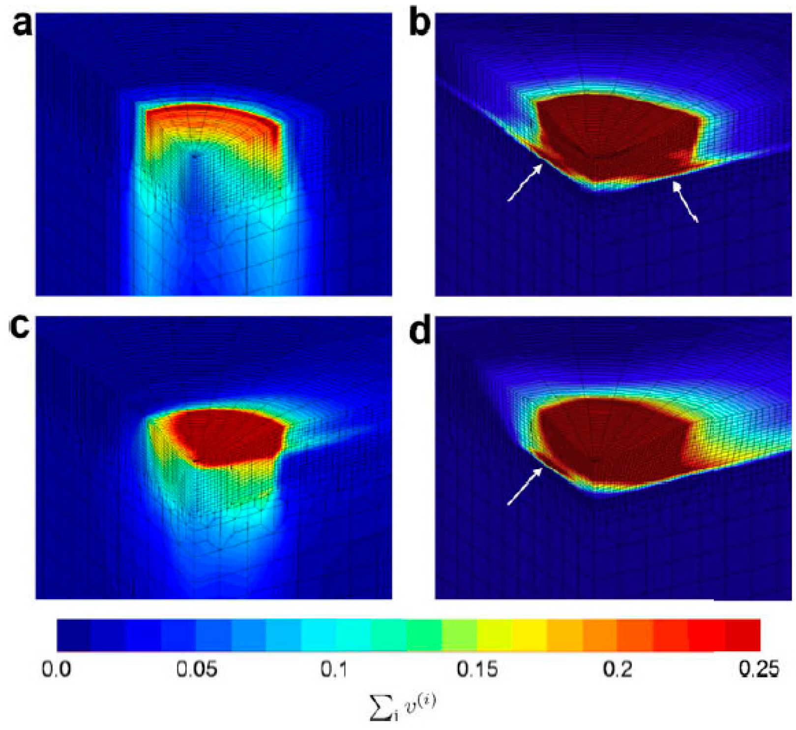
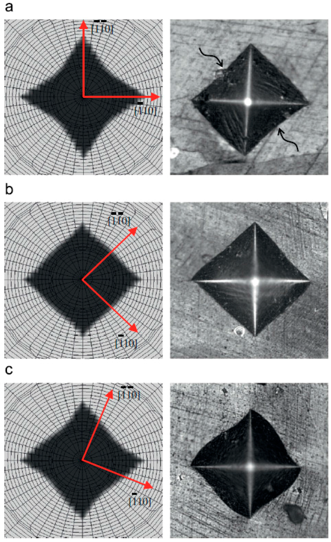
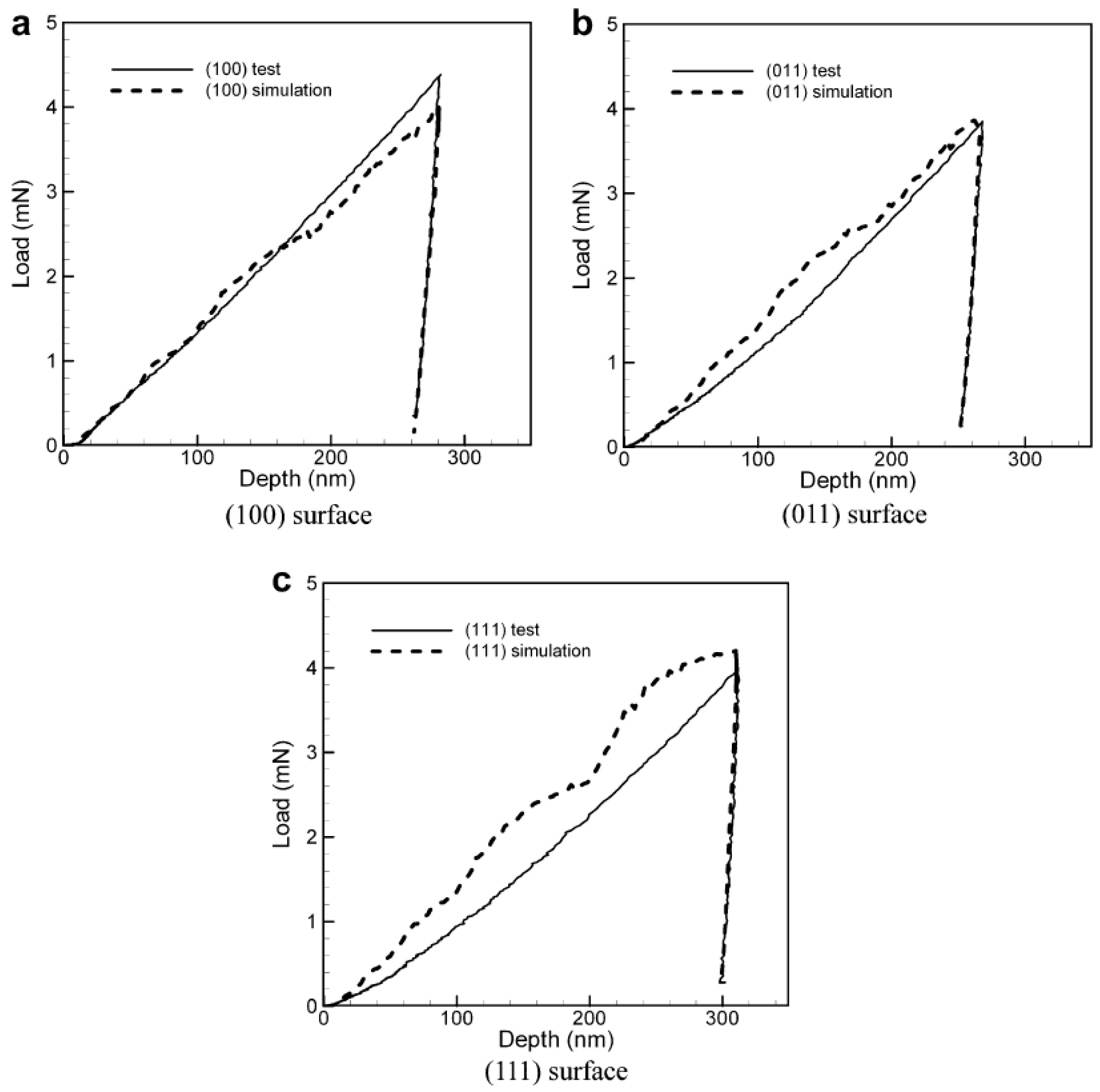
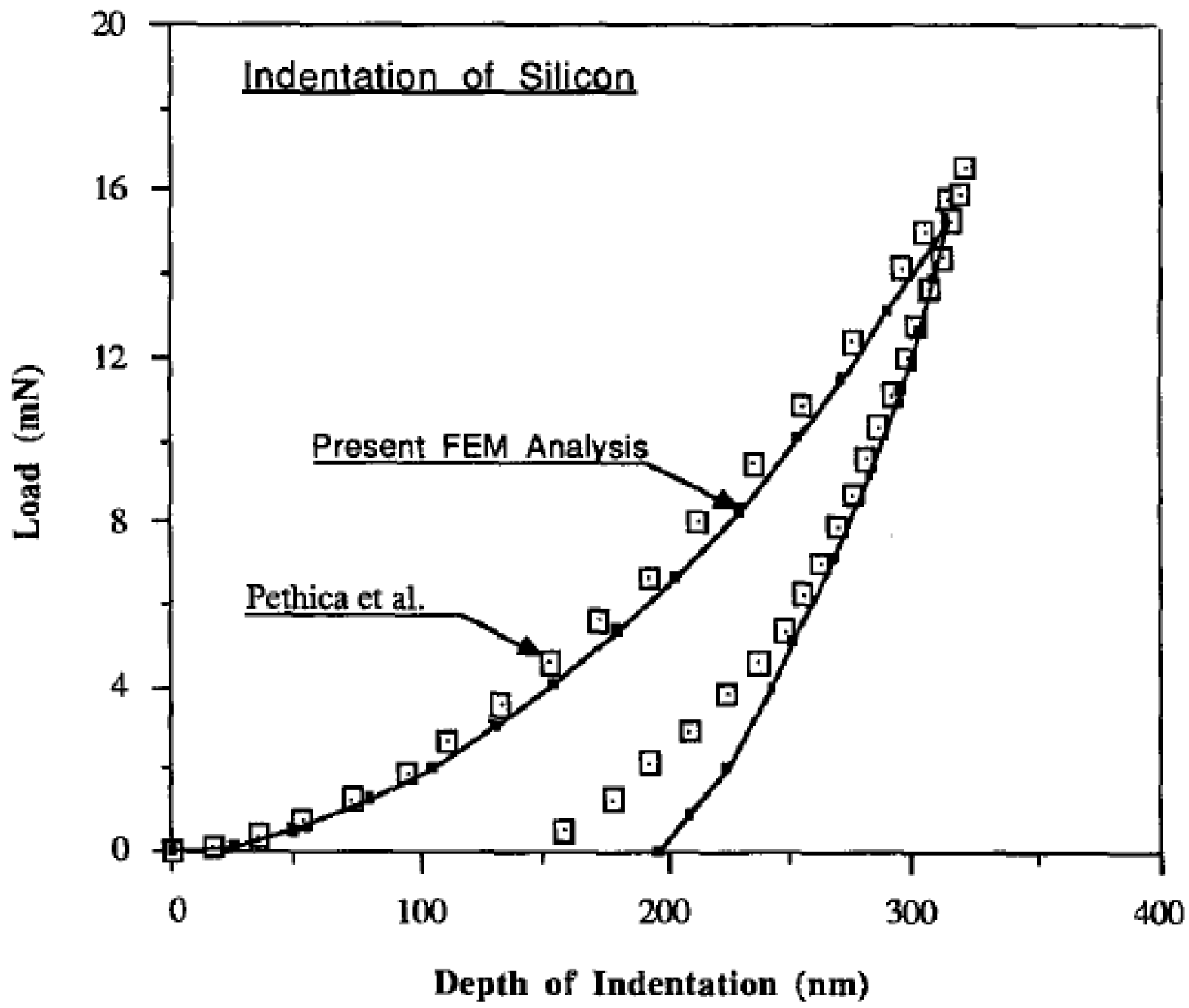
5.1. Conventional Finite Element Method (FEM) Simulations

Lee and Kobayashi’s work [103] was the first to conduct the finite element simulation (FEM) of indentation in 1969. Plane strain and axisymmetric flat punch indentation was simulated to study the development of the plastic zone, the load-displacement relationships, and the stress and strain distributions during continued loading, taking into account the changes of the punch friction and sample dimensions. However, problems such as the accuracy of the solutions and the efficiency of the computation still existed. Then three years later, Lee and his colleagues [83] performed another finite element simulation of indentation using ball indenter, and compared all the results with their own experiments for heat-treated SAE4340 steel. It was found that the simulated load-displacement curve, plastic zone development and indentation pressure were in good agreement with the experimental observations. In addition, by calculating the mean effective strains with FEM, the representative strains defined by Tabor were found to be equal to the mean effective strains of the plastic zone under the indenters shown in Figure 28.
Bhattacharya and Nix [104] performed elastoplastic FEM simulations of nanoindentation using conical indenter to study the elastic and plastic properties of materials on a sub-micro scale under the conditions of frictionless and completely adhesive contact. The simulated load-displacement curves for nickel and silicon were compared with experimental results as shown in Figure 29 and Figure 30, respectively. It was concluded that the FEM is suitable to simulate nanoindentation behaviour at a sub-micro scale for different types of materials. Bhattacharya and Nix [105] then investigated the relationship between Young’s modulus and yield strength, and concluded from FEM simulation that the shapes of the plastic zones for an elastic-plastic bulk material under a conical indenter depend strongly on the ratio E/ σ y (Young’s modulus/yield stress) with a fixed indenter angle as shown in Figure 31.
Subsequently, FEM nanoindentation simulation of thin films [107,108,109,110], stress distribution [111,112,113], hardness [114,115,116], friction effects [109,117], brittle cracking behaviour [118,119,120] and coatings [121,122] were extensively developed.
Furthermore, recently Maier et al. [123,124,125] proposed an inverse analysis method to identify elastic-plastic material parameters via FEM indentation simulation, and their proposed methodology was validated using “pseudo-experimental” (computer generated) data with and without noise. Chen et al. [126] proposed two alternative indentation techniques to effectively distinguish elastoplastic properties of the mystical materials which have distinct elastoplastic properties yet they yield almost identical indentation behaviors, even when the indenter angle is varied in a large range
Most of the researchers thought the conventional plasticity theory cannot be used to explain ISE because its constitutive models possess no intrinsic (internal) material lengths. However, Storakers et al. [127] did observe the reversed ISE through simulation by using a parabola-shaped indenter.

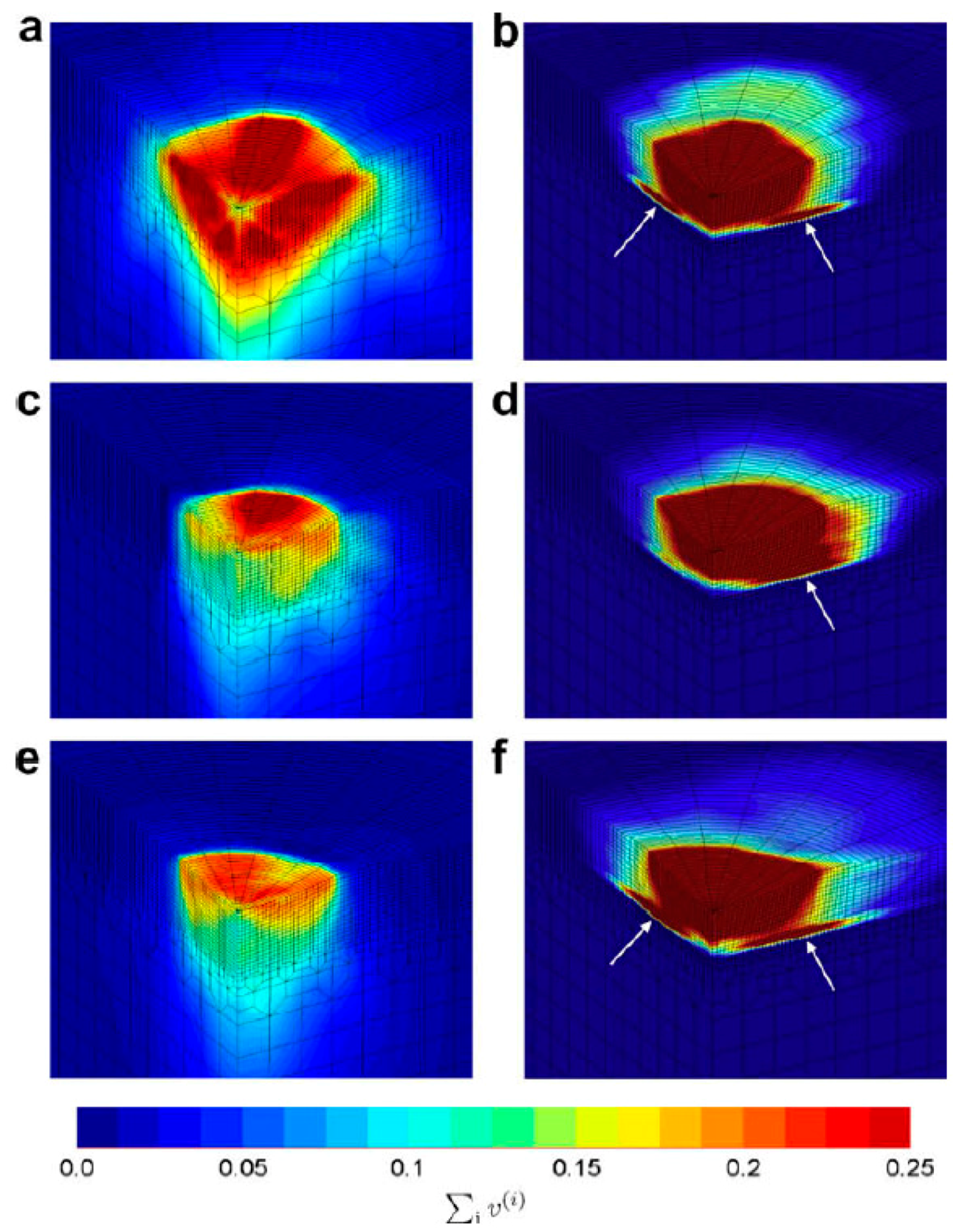
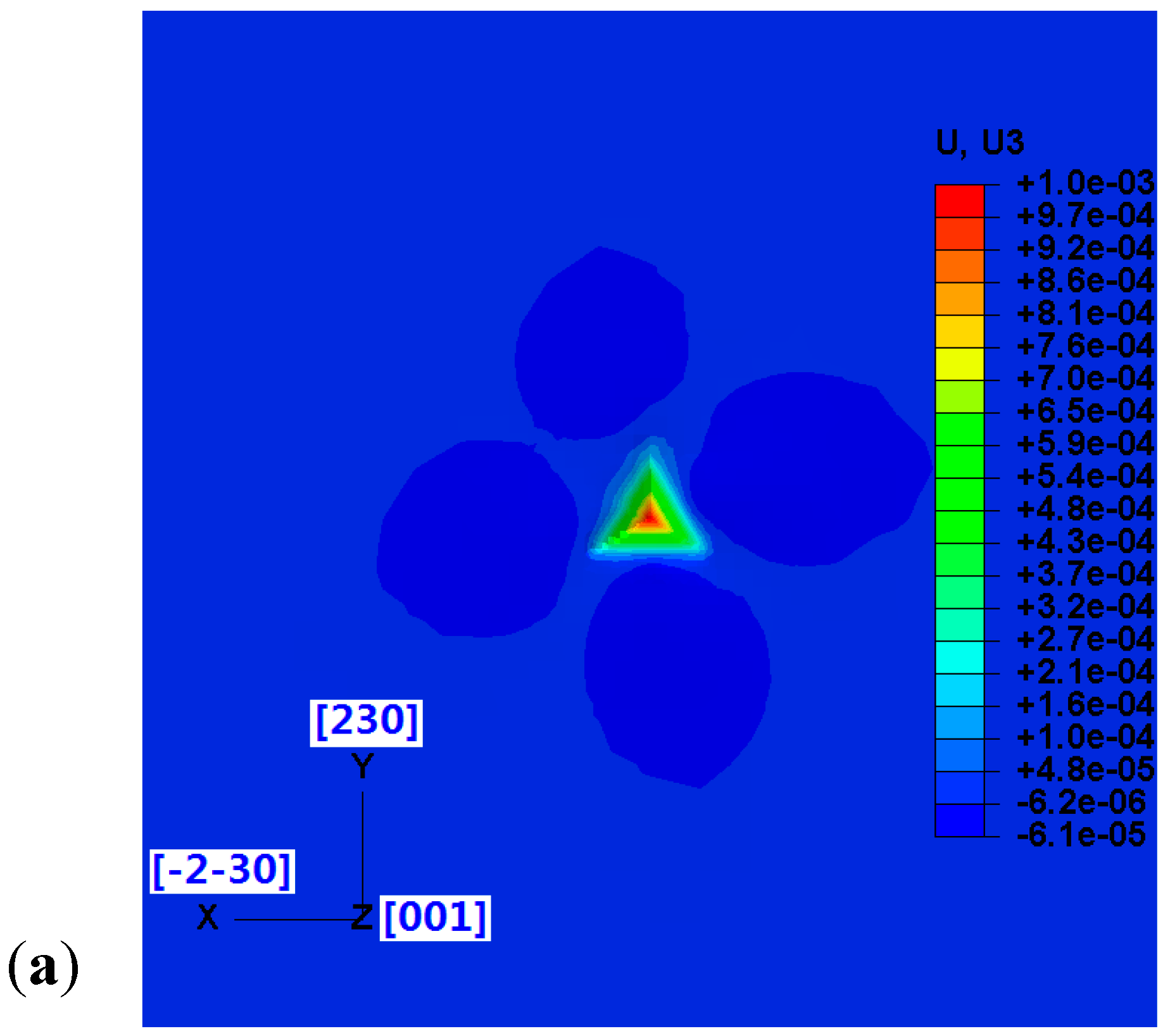
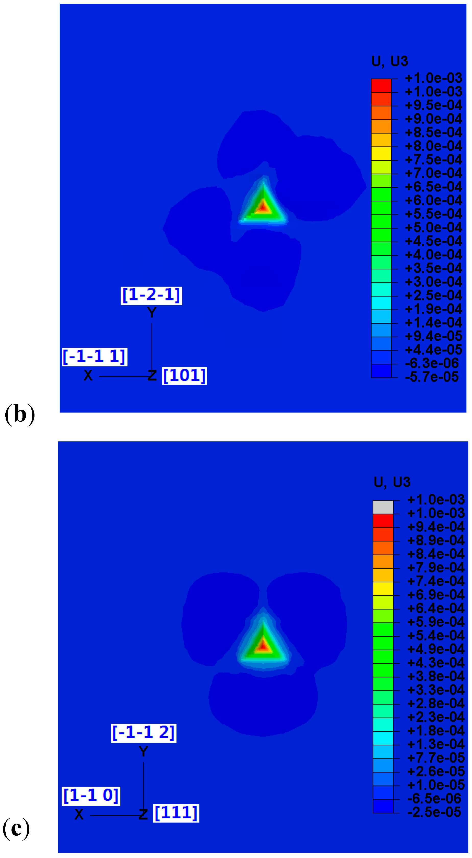
5.2. Crystal Plasticity FEM Simulation

The evolution of crystallographic texture and grain lattice rotation under the indentation has not been well understood. This work must be done through the crystal plasticity based simulation.
Casals and Forest [128] investigated the anisotropy in the contact response of FCC and HCP (hexagonal closest-packed) single crystal via simulating spherical indentation experiments of bulk single crystals and thin films on hard substrates. Their simulations predicted that the plastic zone beneath the indenter preferentially grew along the slip system directions as shown in Figure 32 and Figure 33. Consequently, in coated thin film systems, a prominent localization of plastic deformation occurred at those specific regions where slip system directions intersected the substrate. Meanwhile, these specific areas were prone to crack nucleation in terms of accumulative plastic damage. Therefore, the identification of these areas was meaningful for the prediction of potential delamination and failure of the coatings. Casals et al. [129] also used three-dimensional crystal plasticity finite element simulations to examine Vickers and Berkovich indentation experiments of strain-hardened copper. The results showed that the simulation was in a good agreement with experimental observations with respect to hardness, load-displacement curves, material piling up and sinking in development at the contact boundary.
Alcala et al. [130] analysed Vickers and Berkovich indentation behaviour via extensive crystal plasticity finite element simulation by recourse to the Bassani and Wu hardening model for pure FCC crystals. The simulated results have been used to illustrate the impact of the crystallographic orientation, as shown in Figure 34. It was clear that the irregular appearance of pyramidal indentations was governed by the crystallography of FCC crystals on the indented surface.
Liu et al. [131] implemented crystal plasticity constitutive model initially developed by Peirce et al. [132] in a finite element code Abaqus/Explicit to study the material behaviour of nanoindentation on (001) oriented surface of single crystal copper. All of the appropriate meso-plastic parameters used in the hardening model was determined by fitting the simulated load-displacement curves to the experimental data. Their studies demonstrated that the combined nanoindentation/CPFEM simulation approach for determining meso-plasitc model parameters works reasonably well from micro level to the macro level as shown in Figure 35. They also investigated the orientation effects in nanoindentation of single crystal copper [133]. Simulated load-displacement curves were found to be in agreement with those from experimental tests as shown in Figure 36. Meanwhile, two-, three-, and four-fold symmetric piling-up patterns were observed on (011), (111), and (100) oriented surface with respect to CPFEM simulation. The anisotropic nature of the surface topographies around the imprints in different crystallographic orientations of the single crystal copper samples then were related to the active slip systems and local texture variations. Wang et al. [40] had similar observations while performing a 3D elastic-viscoplastic crystal plasticity finite element method simulation to study the dependence of nanoindentation piling-up patterns. Their simulation showed that the piling-up patterns on the surface of (001)-, (011)- and (111)-oriented single crystal copper had four-, two-, and sixfold symmetry, respectively. All the simulated piling-up patterns were in agreement with those from the experiments. The explanations of the anisotropic surface profiles were also related to the active slip systems and local texture variations.
Zaafarani et al. [45] carried out the 3D elastic-viscoplastic crystal plasticity finite element simulations with the same geometry of indenter and boundary conditions as those from experiments. Their CPFEM simulations predicted a similar pattern for the absolute orientation changes as the experiments as shown in Figure 37. However, it was found that the simulations over-emphasized the magnitude of the rotation field tangent to the indenter relative to that directly below the indenter tip. The reason was then found to be due to edge effects at the contact zone and milling-induced curvature caused by ion beam so that no complete EBSD mapping could be made up to the actual contact interface [134].
Eidel [135] simulated pyramidal micro-indentation on the (001) surface of Ni-base superalloy single crystal with three different azimuthal orientations of the pyramidal indenter. The numerical piling-up patterns were compared with the experimental results. It was found that the resultant material piling-up was insensitive to different azimuthal orientations of the pyramidal indenter as shown in Figure 38. The reason could be due to the piling-up formation determined by crystallographic processes rather than by the stress distribution pattern, induced under the non-isotropic pyramidal indenter. He then also found that the piling-up was independent of the indenter shape (sphere or pyramid) and the elastic anisotropy, which further confirmed that only the geometry of the slip systems in the (001) oriented crystal governed piling-up, whereas stress concentrations introduced by different indenter shapes, by the azimuthal orientation of a pyramidal indenter and also by the characteristics of the elasticity law, had no significant influence.
Liu et al. [136] simulated indentation process of single-crystal aluminium with three different initial orientations via using three-sided Berkovich indenter, and all the numerical load-displacement curves and pile-up patterns from CPFEM have been validated by experimental observations, as shown in Figure 39, Figure 40 and Figure 41. CPFEM simulation was also used to explain the anisotropic feature of pile-up patterns for different single crystals in details [137,138]. Recently, indentation on severely deformed materials [139] and bicrystalline ones [139] were also investigated via CPFEM modelling.

6. Conclusions

Nanoindentation is the most popular method to investigate the mechanical properties of materials at mico- and nanoscale. The key advantage of this technology is its convenience and applicability on a very small sample where normal tensile test cannot be applied. A vast number of experiments have been conducted to investigate different characters during indentation deformation, including hardness, Young’s modulus, load-displacement curve, ISE, piling up and sinking in, cracks, texture evolution and lattice rotation and so on. Meanwhile, a wide range of materials were studied, such as metals, ceramics, rubbers, human bones, coatings, etc.
Indentation size effect has been extensively studied by numerous researchers. Among all of these researchers, Nix and Gao has proposed a strain gradient model which was believed to be the best way to simulate and explain ISE in the past. However, it has been found that the main assumptions for that model are in conflict with the experimental observations. Other potential influence factors, such as inadequate measurement capabilities of extremely small indents, presence of oxides or chemical contamination on the surface, indenter-sample friction, increased dominance of edge effects with shallow indents and tip radius have been eventually proven to be ineffective in determining the ISE. Therefore, the mechanism of ISE needs to be further investigated and discussed.
The conventional FEM has been used to study the indentation process on materials and to predict their hardness, stress distribution, friction effects, Young’s Modulus, load-displacement curves, and brittle cracking behaviour and so on. However, the anisotropic characters of materials could not be taken into account in the conventional FEM. Therefore, Crystal plasticity FEM (CPFEM) which considers the lattice rotation and the plastic slip as the key deformation mechanism has been used to simulate the texture evolution of materials during indentation deformation. All the numerical results can be accurately validated by comparing with experimental observations. In addition, CPFEM is also the best candidate to investigate the deformation mechanism of materials at smaller scale.

Acknowledgments

The authors acknowledge the financial support from an Australian Research Council Discovery Grant (DP0773329) and from UPA and IPTA scholarships from the University of Wollongong and from Japan Society for the Promotion of Science (JSPS).

Conflicts of Interest

The authors declare no conflicts of interest.

References

  1. Tabor, D. The Hardness of Metals; Oxford University Press: Oxford, UK, 1951. [Google Scholar]
  2. Bhushan, B. Handbook of Micro/Nanotribology, 2nd ed.; CRC Press: Boca Raton, FL, USA, 1999. [Google Scholar]
  3. Brinell, J.A. Way of determining the hardness of bodies and some applications of the same. Teknisk Tidskrift 1900, 5, 69. [Google Scholar]
  4. Wahlberg, A. Brinell’s method of determining hardness and other properties of iron and steel. J. Iron. Steel Inst. 1901, 59, 243. [Google Scholar]
  5. Meyer, E. Investigations of hardness testing and hardness. Phys. Z 1908, 9, 66. [Google Scholar]
  6. Smith, R.; Sandland, G. An accurate method of determining the hardness of metals, with particular reference to those of a high degree of hardness. Proc. Inst. Mech. Eng. 1922, 102, 623. [Google Scholar] [CrossRef]
  7. Hutchings, I.M. The contributions of David Tabor to the science of indentation hardness. J. Mater. Res. 2009, 24, 581–589. [Google Scholar] [CrossRef]
  8. Tabor, D. A simple theory of static and dynamic hardness. Proc. R. Soc. Lond. Ser. A 1948, 192, 247–274. [Google Scholar] [CrossRef]
  9. Johnson, K.L. The correlation of indentation experiments. J. Mech. Phys. Solids 1970, 18, 115–126. [Google Scholar] [CrossRef]
  10. King, R.F.; Tabor, D. The effect of temperature on the mechanical properties and the friction of plastics. Proc. Phys. Soc. B 1953, 66, 728–736. [Google Scholar] [CrossRef]
  11. Pascoe, M.W.; Tabor, D. The Friction and Deformation of Polymers. Proc. R. Soc. A 1956, 235, 210–224. [Google Scholar] [CrossRef]
  12. King, R.F.; Tabor, D. The strength properties and frictional behaviour of brittle solids. Proc. R. Soc. A 1954, 223, 225–238. [Google Scholar] [CrossRef]
  13. Atkins, A.G.; Tabor, D. Mutual Indentation Hardness of Single-Crystal Magnesium Oxide at High Temperatures. J. Am. Ceram. Soc. 1967, 50, 195–198. [Google Scholar] [CrossRef]
  14. Fischer-Cripps, A.C. A review of analysis methods for sub-micron indentation testing. Vacuum 2000, 58, 569–585. [Google Scholar] [CrossRef]
  15. Available online: http://www.nanoindentation.cornell.edu/Machine/commercial_machine.htm (accessed on 1 December 2013).
  16. Fischer-Cripps, A.C. The IBIS Handbook of Nanoindentation; Fischer-Cripps Laboratories Pty Ltd.: Sydney, Australia, 2009. [Google Scholar]
  17. Kim, D.K. Nanoindentation Lecture 1 Basic Principle, KAIST: Daejeon, Korea. Available online: http://szft.elte.hu/oktat/www/mikronano/Nano_indentation.pdf (accessed on 17 August 2017).
  18. Oliver, W.C.; Pharr, G.M. An Improved Technique for Determining Hardness and Elastic-Modulus Using Load and Displacement Sensing Indentation Experiments. J. Mater. Res. 1992, 7, 1564–1583. [Google Scholar] [CrossRef]
  19. Oliver, W.C.; Pharr, G.M. Measurement of hardness and elastic modulus by instrumented indentation: Advances in understanding and refinements to methodology. J. Mater. Res. 2004, 19, 3–20. [Google Scholar] [CrossRef]
  20. Kucharski, S.; Mroz, Z. Identification of yield stress and plastic hardening parameters from a spherical indentation test. Int. J. Mech. Sci. 2007, 49, 1238–1250. [Google Scholar] [CrossRef]
  21. Kruzic, J.J.; Kim, D.K.; Koester, K.J.; Ritchie, R.O. Indentation techniques for evaluating the fracture toughness of biomaterials and hard tissues. J. Mech. Behav. Biomed. 2009, 2, 384–395. [Google Scholar] [CrossRef] [PubMed]
  22. Huber, N.; Tsakmakis, C. Experimental and theoretical investigation of the effect of kinematic hardening on spherical indentation. Mech. Mater. 1998, 27, 241–248. [Google Scholar] [CrossRef]
  23. Masri, R.; Durban, D. Cylindrical cavity expansion in compressible Mises and Tresca solids. Eur. J. Mech. A-Solids 2007, 26, 712–727. [Google Scholar] [CrossRef]
  24. Mata, M.; Anglada, M.; Alcala, J. A hardness equation for sharp indentation of elastic-power-law strain-hardening materials. Philos. Mag. A 2002, 82, 1831–1839. [Google Scholar] [CrossRef]
  25. Hill, R. The Mathematical Theory of Plasticity; Oxford University Press: Oxford, UK, 1950. [Google Scholar]
  26. Marsh, D.M. Plastic Flow in Glass. Proc. R. Soc. A 1964, 279, 420–435. [Google Scholar] [CrossRef]
  27. Rodriguez, J.; Rico, A.; Otero, E.; Rainforth, W.M. Indentation properties of plasma sprayed Al2O3-13% TiO2 nanocoatings. Acta Mater. 2009, 57, 3148–3156. [Google Scholar] [CrossRef]
  28. Mencik, J.; Munz, D.; Quandt, E.; Weppelmann, E.R.; Swain, M.V. Determination of elastic modulus of thin layers using nanoindentation. J. Mater. Res. 1997, 12, 2475–2484. [Google Scholar] [CrossRef]
  29. Swain, M.V.; Mencik, J. Mechanical Property Characterization of Thin-Films Using Spherical Tipped Indenters. Thin Solid Films 1994, 253, 204–211. [Google Scholar] [CrossRef]
  30. Jonsson, B.; Hogmark, S. Hardness Measurements of Thin-Films. Thin Solid Films 1984, 114, 257–269. [Google Scholar] [CrossRef]
  31. Opitz, A.; Ahmed, S.I.U.; Schaefer, J.A.; Scherge, M. Nanofriction of silicon oxide surfaces covered with thin water films. Wear 2003, 254, 924–929. [Google Scholar] [CrossRef]
  32. Kim, J.H.; Yeon, S.C.; Jeon, Y.K.; Kim, J.G.; Kim, Y.H. Nano-indentation method for the measurement of the Poisson’s ratio of MEMS thin films. Sens. Actuator A-Phys. 2003, 108, 20–27. [Google Scholar] [CrossRef]
  33. Lou, J.; Shrotriya, P.; Buchheit, T.; Yang, D.; Soboyejo, W.O. Nanoindentation study of plasticity length scale effects in LIGA Ni microelectromechanical systems structures. J. Mater. Res. 2003, 18, 719–728. [Google Scholar] [CrossRef]
  34. Chicot, D.; Demarecaux, P.; Lesage, J. Apparent interface toughness of substrate and coating couples from indentation tests. Thin Solid Films 1996, 283, 151–157. [Google Scholar] [CrossRef]
  35. Drory, M.D.; Hutchinson, J.W. Measurement of the adhesion of a brittle film on a ductile substrate by indentation. Proc. R. Soc. Lond. A 1953, 452, 2319–2341. [Google Scholar] [CrossRef]
  36. Yamazaki, Y.; Kuga, S.; Yoshida, T. Evaluation of interfacial strength by an instrumented indentation method and its application to an actual TBC vane. Acta Metall. Sin.-Engl. 2011, 24, 109–117. [Google Scholar]
  37. Bartsch, M.; Mircea, I.; Suffner, J.; Baufeld, B. Interfacial fracture toughness measurement of thick ceramic coatings by indentation. Key Eng. Mater. 2005, 290, 183–190. [Google Scholar] [CrossRef]
  38. Vasinonta, A.; Beuth, J.L. Measurement of interfacial toughness in thermal barrier coating systems by indentation. Eng. Fract. Mech. 2001, 68, 843–860. [Google Scholar] [CrossRef]
  39. Yamazaki, Y.; Kuga, S.-I.; Jayaprakash, M. Interfacial Strength Evaluation Technique for Thermal Barrier Coated Components by Using Indentation Method. Procedia Eng. 2011, 10, 845–850. [Google Scholar] [CrossRef]
  40. Wang, Y.; Raabe, D.; Kluber, C.; Roters, F. Orientation dependence of nanoindentation pile-up patterns and of nanoindentation microtextures in copper single crystals. Acta Mater. 2004, 52, 2229–2238. [Google Scholar] [CrossRef]
  41. Saka, H.; Nagaya, G. Plan-View Transmission Electron-Microscopy Observation of a Crack-Tip in Silicon. Philos. Mag. Lett. 1995, 72, 251–255. [Google Scholar] [CrossRef]
  42. Lloyd, S.J.; Castellero, A.; Giuliani, F.; Long, Y.; McLaughlin, K.K.; Molina-Aldareguia, J.M.; Stelmashenko, N.A.; Vandeperre, L.J.; Clegg, W.J. Observations of nanoindents via cross-sectional transmission electron microscopy: A survey of deformation mechanisms. Proc. R. Soc. A-Math. Phys. 2005, 461, 2521–2543. [Google Scholar] [CrossRef]
  43. Lloyd, S.J.; Molina-Aldareguia, J.M.; Clegg, W.J. Deformation under nanoindents in sapphire, spinel and magnesia examined using transmission electron microscopy. Philos. Mag. A 2002, 82, 1963–1969. [Google Scholar] [CrossRef]
  44. Rester, M.; Motz, C.; Pippan, R. Indentation across size scales—A survey of indentation-induced plastic zones in copper {111} single crystals. Scr. Mater. 2008, 59, 742–745. [Google Scholar] [CrossRef]
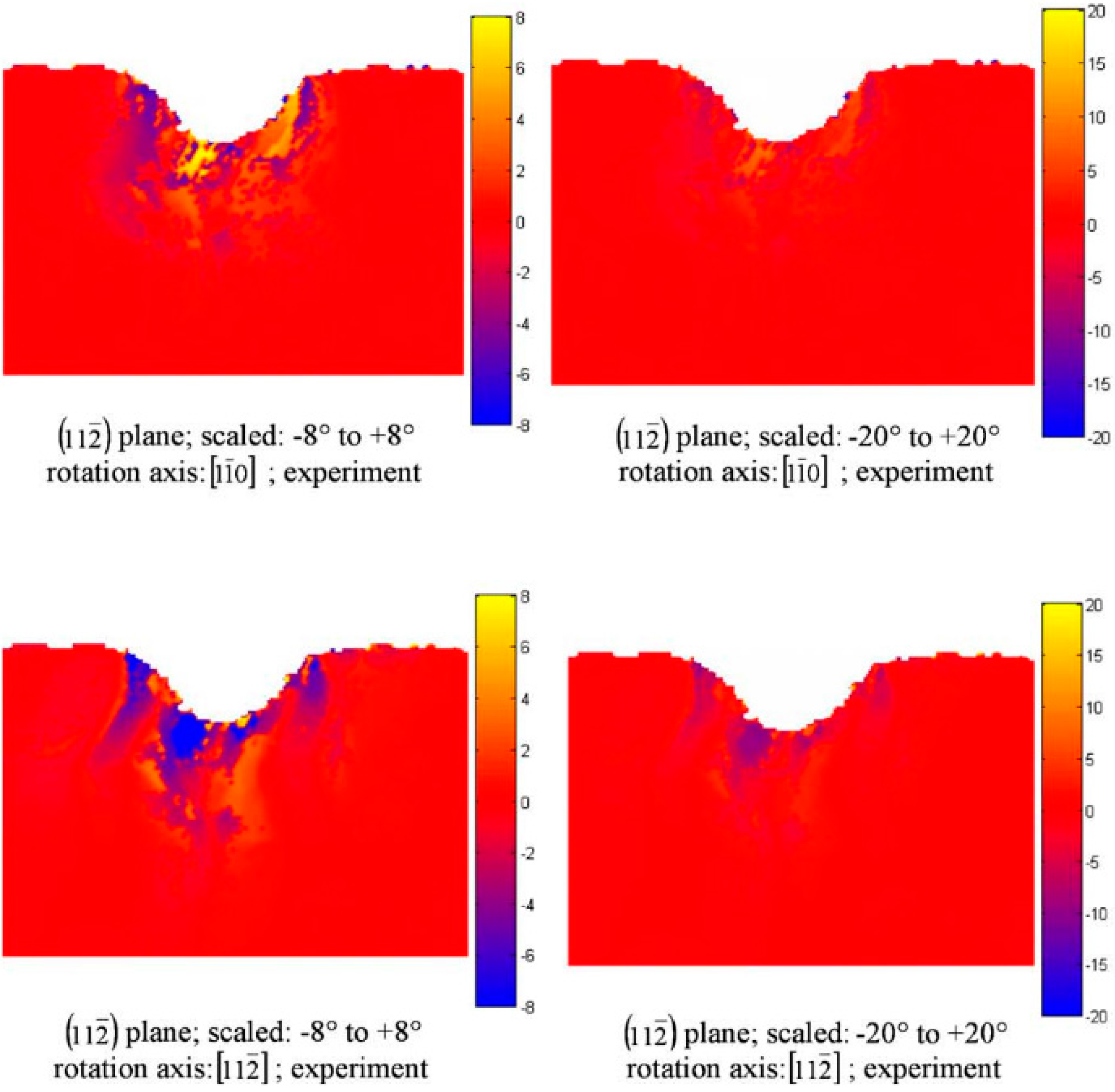
  45. Zaafarani, N.; Raabe, D.; Singh, R.N.; Roters, F.; Zaefferer, S. Three-dimensional investigation of the texture and microstructure below a nanoindent in a Cu single crystal using 3D EBSD and crystal plasticity finite element simulations. Acta Mater. 2006, 54, 1863–1876. [Google Scholar] [CrossRef]
  46. Pharr, G.M.; Herbert, E.G.; Gao, Y.F. The Indentation Size Effect: A Critical Examination of Experimental Observations and Mechanistic Interpretations. Annu. Rev. Mater. Res. 2010, 40, 271–292. [Google Scholar] [CrossRef]
  47. Li, L.; Zhou, Q.; Zhou, Y.Y.; Cao, J.G. Numerical study on the size effect in the ultra-thin sheet’s micro-bending forming process. Mater. Sci. Eng. A 2009, 499, 32–35. [Google Scholar] [CrossRef]
  48. Fleck, N.A.; Muller, G.M.; Ashby, M.F.; Hutchinson, J.W. Strain Gradient Plasticity—Theory and Experiment. Acta Metall. Mater. 1994, 42, 475–487. [Google Scholar] [CrossRef]
  49. Stolken, J.S.; Evans, A.G. A microbend test method for measuring the plasticity length scale. Acta Mater. 1998, 46, 5109–5115. [Google Scholar] [CrossRef]
  50. Gau, J.T.; Principe, C.; Yu, M. Springback behavior of brass in micro sheet forming. J. Mater. Process. Technol. 2007, 191, 7–10. [Google Scholar] [CrossRef]
  51. Geiger, M.; Kleiner, M.; Eckstein, R.; Tiesler, N.; Engel, U. Microforming. CIRP Ann.-Manuf. Technol. 2001, 50, 445–462. [Google Scholar] [CrossRef]
  52. Kals, T.A.; Eckstein, R. Miniaturization in sheet metal working. J. Mater. Process. Technol. 2000, 103, 95–101. [Google Scholar] [CrossRef]
  53. Saotome, Y.; Yasuda, K.; Kaga, H. Microdeep drawability of very thin sheet steels. J. Mater. Process. Technol. 2001, 113, 641–647. [Google Scholar] [CrossRef]
  54. Mott, B.W. Microindentation Hardness Testing; Butterworths Scientific Publications: London, UK, 1956. [Google Scholar]
  55. Bückle, H. Progress in micro-indentation hardness testing. Metall. Rev. 1959, 4, 49–100. [Google Scholar] [CrossRef]
  56. Gane, N. Direct Measurement of Strength of Metals on a Sub-Micrometre Scale. Proc. R. Soc. Lond. Ser.-A 1970, 317. [Google Scholar] [CrossRef]
  57. Kiener, D.; Durst, K.; Rester, M.; Minor, A.M. Revealing deformation mechanisms with nanoindentation. JOM-US 2009, 61, 14–23. [Google Scholar] [CrossRef]
  58. Gerberich, W.W.; Tymiak, N.I.; Grunlan, J.C.; Horstemeyer, M.F.; Baskes, M.I. Interpretations of indentation size effects. J. Appl. Mech. 2002, 69, 433–442. [Google Scholar] [CrossRef]
  59. Bull, S.J. On the origins and mechanisms of the indentation size effect. Z. Metallkd. 2003, 94, 787–792. [Google Scholar] [CrossRef]
  60. Zhu, T.T.; Bushby, A.J.; Dunstan, D.J. Materials mechanical size effects: A review. Mater. Technol. 2008, 23, 193–209. [Google Scholar] [CrossRef]
  61. Sangwal, K. On the reverse indentation size effect and microhardness measurement of solids. Mater. Chem. Phys. 2000, 63, 145–152. [Google Scholar] [CrossRef]
  62. Voyiadjis, G.Z.; Peters, R. Size effects in nanoindentation: An experimental and analytical study. Acta Mech. 2010, 211, 131–153. [Google Scholar] [CrossRef]
  63. Ashby, M.F. Deformation of Plastically Non-Homogeneous Materials. Philos. Mag. 1970, 21, 399–424. [Google Scholar] [CrossRef]
  64. Nye, J.F. Some geometrical relations in dislocated crystals. Acta Metall. Mater. 1953, 1, 153–162. [Google Scholar] [CrossRef]
  65. Nix, W.D.; Gao, H.J. Indentation size effects in crystalline materials: A law for strain gradient plasticity. J. Mech. Phys. Solids 1998, 46, 411–425. [Google Scholar] [CrossRef]
  66. Wiedersich, H. Hardening mechanisms and the theory of deformation. JOM 1964, 16, 425–430. [Google Scholar]
  67. Ebisu, T.; Horibe, S. Analysis of the indentation size effect in brittle materials from nanoindentation load-displacement curve. J. Eur. Ceram. Soc. 2010, 30, 2419–2426. [Google Scholar] [CrossRef]
  68. Ma, Q.; Clarke, D.R. Size dependent hardness of silver single crystals. J. Mater. Res. 1995, 10, 853–863. [Google Scholar] [CrossRef]
  69. Poole, W.J.; Ashby, M.F.; Fleck, N.A. Micro-hardness of annealed and work-hardened copper polycrystals. Scr. Mater. 1996, 34, 559–564. [Google Scholar] [CrossRef]
  70. Stelmashenko, N.A.; Walls, M.G.; Brown, L.M.; Milman, Y.V. Microindentations on W and Mo Oriented Single-Crystals—An Stm Study. Acta Metall. Mater. 1993, 41, 2855–2865. [Google Scholar] [CrossRef]
  71. Gao, H.; Huang, Y.; Nix, W.D. Modeling plasticity at the micrometer scale. Naturwissenschaften 1999, 86, 507–515. [Google Scholar] [CrossRef] [PubMed]
  72. Gao, H.; Huang, Y.; Nix, W.D.; Hutchinson, J.W. Mechanism-based strain gradient plasticity—I. Theory. J. Mech. Phys. Solids 1999, 47, 1239–1263. [Google Scholar] [CrossRef]
  73. Acharya, A.; Bassani, J.L. Lattice incompatibility and a gradient theory of crystal plasticity. J. Mech. Phys. Solids 2000, 48, 1565–1595. [Google Scholar] [CrossRef]
  74. Huang, Y.; Gao, H.; Nix, W.D.; Hutchinson, J.W. Mechanism-based strain gradient plasticity—II. Analysis. J. Mech. Phys. Solids 2000, 48, 99–128. [Google Scholar] [CrossRef]
  75. Gurtin, M.E. A gradient theory of single-crystal viscoplasticity that accounts for geometrically necessary dislocations. J. Mech. Phys. Solids 2002, 50, 5–32. [Google Scholar] [CrossRef]
  76. Demir, E.; Raabe, D.; Zaafarani, N.; Zaefferer, S. Investigation of the indentation size effect through the measurement of the geometrically necessary dislocations beneath small indents of different depths using EBSD tomography. Acta Mater. 2009, 57, 559–569. [Google Scholar] [CrossRef]
  77. Rester, M.; Motz, C.; Pippan, R. Microstructural investigation of the volume beneath nanoindentations in copper. Acta Mater. 2007, 55, 6427–6435. [Google Scholar] [CrossRef]
  78. Kiener, D.; Pippan, R.; Motz, C.; Kreuzer, H. Microstructural evolution of the deformed volume beneath microindents in tungsten and copper. Acta Mater. 2006, 54, 2801–2811. [Google Scholar] [CrossRef]
  79. Durst, K.; Backes, B.; Goken, M. Indentation size effect in metallic materials: Correcting for the size of the plastic zone. Scr. Mater. 2005, 52, 1093–1097. [Google Scholar] [CrossRef]
  80. Smedskjaer, M.M. Indentation size effect and the plastic compressibility of glass. Appl. Phys. Lett. 2014, 104, 251906. [Google Scholar] [CrossRef]
  81. Liu, M.; Xu, W.; Bai, J.; Chua, C.K.; Wei, J.; Li, Z.; Gao, Y.; Kim, D.H.; Zhou, K. Investigation of the size effect for photonic crystals. Nanotechnology 2016, 27, 405703. [Google Scholar] [CrossRef] [PubMed]
  82. Onitsch, E.M. The present status of testing the hardness of materials. Mikroskopie 1956, 95, 12–14. [Google Scholar]
  83. Lee, C.H.; Masaki, S.; Kobayashi, S. Analysis of ball indentation. Int. J. Mech. Sci. 1972, 14, 417–426. [Google Scholar] [CrossRef]
  84. Fischer-Cripps, A.C. Critical review of analysis and interpretation of nanoindentation test data. Surf. Coat. Technol. 2006, 200, 4153–4165. [Google Scholar] [CrossRef]
  85. Sakai, M. Energy principle of the indentation-induced inelastic surface deformation and hardness of brittle materials. Acta Metall. Mater. 1993, 41, 1751–1758. [Google Scholar] [CrossRef]
  86. Gong, J.; Wu, J.; Guan, Z. Examination of the indentation size effect in low-load vickers hardness testing of ceramics. J. Eur. Ceram. Soc. 1999, 19, 2625–2631. [Google Scholar] [CrossRef]
  87. Ren, X.J.; Hooper, R.M.; Griffiths, C.; Henshall, J.L. Indentation size effect in ceramics: Correlation with H/E. J. Mater. Sci. Lett. 2003, 22, 1105–1106. [Google Scholar] [CrossRef]
  88. Gogotsi, G.A.; Dub, S.N.; Lomonova, E.E.; Ozersky, B.I. Vickers and Knoop Indentation Behavior of Cubic and Partially-Stabilized Zirconia Crystals. J. Eur. Ceram. Soc. 1995, 15, 405–413. [Google Scholar] [CrossRef]
  89. Sahin, O.; Uzun, O.; Sopicka-Lizer, M.; Gocmez, H.; Kolemen, U. Analysis of load-penetration depth data using Oliver-Pharr and Cheng-Cheng methods of SiAlON-ZrO(2) ceramics. J. Phys. D Appl. Phys. 2008, 41, 035305. [Google Scholar] [CrossRef]
  90. Kolemen, U. Analysis of ISE in microhardness measurements of bulk MgB2 superconductors using different models. J. Alloy Compd. 2006, 425, 429–435. [Google Scholar] [CrossRef]
  91. Peng, Z.; Gong, J.; Miao, H. On the description of indentation size effect in hardness testing for ceramics: Analysis of the nanoindentation data. J. Eur. Ceram. Soc. 2004, 24, 2193–2201. [Google Scholar] [CrossRef]
  92. Gong, J.H.; Zhao, Z.; Guan, Z.D.; Miao, H.Z. Load-dependence of Knoop hardness of Al2O3-TiC composites. J. Eur. Ceram. Soc. 2000, 20, 1895–1900. [Google Scholar] [CrossRef]
  93. Li, H.; Bradt, R.C. The Microhardness Indentation Load Size Effect in Rutile and Cassiterite Single-Crystals. J. Mater. Sci. 1993, 28, 917–926. [Google Scholar] [CrossRef]
  94. Samuels, L.E. Microindentation in Metals; ASTM STP: Philadelphia, PA, USA, 1986; pp. 5–25. [Google Scholar]
  95. Sargent, P.M. Use of the Indentation Size Effect on Microhardness for Materials Characterization; ASTM STP: Philadelphia, PA, USA, 1986; pp. 160–174. [Google Scholar]
  96. Li, H.; Ghosh, A.; Han, Y.H.; Bradt, R.C. The Frictional Component of the Indentation Size Effect in Low Load Microhardness Testing. J. Mater. Res. 1993, 8, 1028–1032. [Google Scholar] [CrossRef]
  97. Elmustafa, A.A.; Stone, D.S. Nanoindentation and the indentation size effect: Kinetics of deformation and strain gradient plasticity. J. Mech. Phys. Solids 2003, 51, 357–381. [Google Scholar] [CrossRef]
  98. Hassel, A.W.; Lohrengel, M.M. Preparation and properties of ultra thin anodic valve metal oxide films. Passiv. Met. Semicond. 1995, 185, 581–590. [Google Scholar] [CrossRef]
  99. McElhaney, K.W.; Vlassak, J.J.; Nix, W.D. Determination of indenter tip geometry and indentation contact area for depth-sensing indentation experiments. J. Mater. Res. 1998, 13, 1300–1306. [Google Scholar] [CrossRef]
  100. Xue, Z.; Huang, Y.; Hwang, K.C.; Li, M. The influence of indenter tip radius on the micro-indentation hardness. J. Eng. Mater. Technol. 2002, 124, 371–379. [Google Scholar] [CrossRef]
  101. Lilleodden, E.T. Indentation-Induced Plasticity of Thin Metal Films. Ph.D. Thesis, Stanford University, Palo Alto, CA, USA, 2001. [Google Scholar]
  102. Huang, Y.; Xue, Z.; Gao, H.; Nix, W.D.; Xia, Z.C. A Study of Microindentation Hardness Tests by Mechanism-based Strain Gradient Plasticity. J. Mater. Res. 2000, 15, 1786–1796. [Google Scholar] [CrossRef]
  103. Lee, C.H.; Kobayash, S. Elastoplastic Analysis of Plane-Strain and Axisymmetric Flat Punch Indentation by Finite-Element Method. Int. J. Mech. Sci. 1970, 12, 349–370. [Google Scholar] [CrossRef]
  104. Bhattacharya, A.K.; Nix, W.D. Finite-Element Simulation of Indentation Experiments. Int. J. Solids Struct. 1988, 24, 881–891. [Google Scholar] [CrossRef]
  105. Bhattacharya, A.K.; Nix, W.D. Finite-Element Analysis of Cone Indentation. Int. J. Solids Struct. 1991, 27, 1047–1058. [Google Scholar] [CrossRef]
  106. Pethica, J.B.; Hutchings, R.; Oliver, W.C. Hardness Measurement at Penetration Depths as Small as 20-Nm. Philos. Mag. A 1983, 48, 593–606. [Google Scholar] [CrossRef]
  107. Lichinchi, M.; Lenardi, C.; Haupt, J.; Vitali, R. Simulation of Berkovich nanoindentation experiments on thin films using finite element method. Thin Solid Films 1998, 312, 240–248. [Google Scholar] [CrossRef]
  108. Bressan, J.D.; Tramontin, A.; Rosa, C. Modeling of nanoindentation of bulk and thin film by finite element method. Wear 2005, 258, 115–122. [Google Scholar] [CrossRef]
  109. Huang, X.Q.; Pelegri, A.A. Finite element analysis on nanoindentation with friction contact at the film/substrate interface. Compos. Sci. Technol. 2007, 67, 1311–1319. [Google Scholar] [CrossRef]
  110. Pelletier, H.; Krier, J.; Cornet, A.; Mille, P. Limits of using bilinear stress-strain curve for finite element modeling of nanoindentation response on bulk materials. Thin Solid Films 2000, 379, 147–155. [Google Scholar] [CrossRef]
  111. Xu, B.; Zhao, B.; Yue, Z.F. Finite element analysis of the indentation stress characteristics of the thin film/substrate systems by flat cylindrical indenters. Mater. Werkst. 2006, 37, 681–686. [Google Scholar] [CrossRef]
  112. Care, G.; FischerCripps, A.C. Elastic-plastic indentation stress fields using the finite-element method. J. Mater. Sci. 1997, 32, 5653–5659. [Google Scholar] [CrossRef]
  113. Zhao, M.H.; Yao, L.P.; Zhang, T.Y. Stress analysis of microwedge indentation-induced delamination. J. Mater. Res. 2009, 24, 1943–1949. [Google Scholar] [CrossRef]
  114. Wang, H.F.; Yang, X.; Bangert, H.; Torzicky, P.; Wen, L. 2-Dimensional Finite-Element Method Simulation of Vickers Indentation of Hardness Measurements on Tin-Coated Steel. Thin Solid Films 1992, 214, 68–73. [Google Scholar] [CrossRef]
  115. Yan, W.Y.; Sun, Q.P.; Liu, H.Y. Spherical indentation hardness of shape memory alloys. Mater. Sci. Eng. A-Struct. 2006, 425, 278–285. [Google Scholar] [CrossRef]
  116. Toparli, M.; Koksal, N.S. Hardness and yield strength of dentin from simulated nano-indentation tests. Comput. Methods Prog. Biomed. 2005, 77, 253–257. [Google Scholar] [CrossRef] [PubMed]
  117. Sarris, E.; Constantinides, G. Finite element modeling of nanoindentation on C-S-H: Effect of pile-up and contact friction. Cem. Concr. Comp. 2013, 36, 78–84. [Google Scholar] [CrossRef]
  118. Niezgoda, T.; Malachowski, J.; Boniecki, M. Finite element simulation of vickers microindentation on alumina ceramics. Ceram. Int. 1998, 24, 359–364. [Google Scholar] [CrossRef]
  119. Larsson, P.L.; Giannakopoulos, A.E. Tensile stresses and their implication to cracking at pyramid indentation of pressure-sensitive hard metals and ceramics. Mater. Sci. Eng. A-Struct. 1998, 254, 268–281. [Google Scholar] [CrossRef]
  120. Wang, H.F.; Bangert, H. 3-Dimensional Finite-Element Simulation of Vickers Indentation on Coated Systems. Mater. Sci. Eng. A-Struct. 1993, 163, 43–50. [Google Scholar] [CrossRef]
  121. Zhai, J.G.; Wang, Y.Q.; Kim, T.G.; Song, J.I. Finite element and experimental analysis of Vickers indentation testing on Al2O3 with diamond-like carbon coating. J. Cent. South Univ. 2012, 19, 1175–1181. [Google Scholar] [CrossRef]
  122. Chen, Z.Y.; Diebels, S. Nanoindentation of hyperelastic polymer layers at finite deformation and parameter re-identification. Arch. Appl. Mech. 2012, 82, 1041–1056. [Google Scholar] [CrossRef]
  123. Bolzon, G.; Maier, G.; Panico, M. Material model calibration by indentation, imprint mapping and inverse analysis. Int. J. Solids Struct. 2004, 41, 2957–2975. [Google Scholar] [CrossRef]
  124. Bocciarelli, M.; Bolzon, G.; Maier, G. Parameter identification in anisotropic elastoplasticity by indentation and imprint mapping. Mech. Mater. 2005, 37, 855–868. [Google Scholar] [CrossRef]
  125. Nakamura, T.; Wang, T.; Sampath, S. Determination of properties of graded materials by inverse analysis and instrumented indentation. Acta Mater. 2000, 48, 4293–4306. [Google Scholar] [CrossRef]
  126. Chen, X.; Ogasawara, N.; Zhao, M.H.; Chiba, N. On the uniqueness of measuring elastoplastic properties from indentation: The indistinguishable mystical materials. J. Mech. Phys. Solids 2007, 55, 1618–1660. [Google Scholar] [CrossRef]
  127. Storåkers, B.; Biwa, S.; Larsson, P.-L. Similarity analysis of inelastic contact. Int. J. Solids Struct. 1997, 34, 3061–3083. [Google Scholar] [CrossRef]
  128. Casals, O.; Forest, S. Finite element crystal plasticity analysis of spherical indentation in bulk single crystals and coatings. Comput. Mater. Sci. 2009, 45, 774–782. [Google Scholar] [CrossRef]
  129. Casals, O.; Ocenasek, J.; Alcala, J. Crystal plasticity finite element simulations of pyramidal indentation in copper single crystals. Acta Mater. 2007, 55, 55–68. [Google Scholar] [CrossRef]
  130. Alcala, J.; Casals, O.; Ocenasek, J. Micromechanics of pyramidal indentation in fcc metals: Single crystal plasticity finite element analysis. J. Mech. Phys. Solids 2008, 56, 3277–3303. [Google Scholar] [CrossRef]
  131. Liu, Y.; Wang, B.; Yoshino, M.; Roy, S.; Lu, H.; Komanduri, R. Combined numerical simulation and nanoindentation for determining mechanical properties of single crystal copper at mesoscale. J. Mech. Phys. Solids 2005, 53, 2718–2741. [Google Scholar] [CrossRef]
  132. Peirce, D.; Asaro, R.J.; Needleman, A. An Analysis of Nonuniform and Localized Deformation in Ductile Single-Crystals. Acta Metall. Mater. 1982, 30, 1087–1119. [Google Scholar] [CrossRef]
  133. Liu, Y.; Varghese, S.; Ma, J.; Yoshino, M.; Lu, H.; Komanduri, R. Orientation effects in nanoindentation of single crystal copper. Int. J. Plast. 2008, 24, 1990–2015. [Google Scholar] [CrossRef]
  134. Zaafarani, N.; Raabe, D.; Roters, F.; Zaefferer, S. On the origin of deformation-induced rotation patterns below nanoindents. Acta Mater. 2008, 56, 31–42. [Google Scholar] [CrossRef]
  135. Eidel, B. Crystal plasticity finite-element analysis versus experimental results of pyramidal indentation into (0 0 1) fcc single crystal. Acta Mater. 2011, 59, 1761–1771. [Google Scholar] [CrossRef]
  136. Liu, M.; Lu, C.; Tieu, K.A.; Peng, C.T.; Kong, C. A combined experimental-numerical approach for determining mechanical properties of aluminum subjects to nanoindentation. Sci. Rep. 2015, 14, 15072. [Google Scholar] [CrossRef] [PubMed]
  137. Liu, M.; Tieu, K.A.; Zhou, K.; Peng, C.T. Investigation of the Anisotropic Mechanical Behaviors of Copper Single Crystals through Nanoindentation Modeling. Metall. Mater. Trans. A 2016, 47, 2717–2725. [Google Scholar] [CrossRef]
  138. Liu, M.; Tieu, A.K.; Peng, C.T.; Zhou, K. Explore the anisotropic indentation pile-up patterns of single-crystal coppers by crystal plasticity finite element modelling. Mater. Lett. 2015, 161, 227–230. [Google Scholar] [CrossRef]
  139. Liu, M.; Tieu, K.A.; Zhou, K.; Peng, C.T. Indentation analysis of mechanical behaviour of torsion-processed single-crystal copper by crystal plasticity finite-element method modelling. Philos. Mag. 2016, 96, 261–273. [Google Scholar] [CrossRef]
Figure 1. Commonly used methods of indentation hardness tests: (a) spherical indenter (Brinell and Meyer); (b) diamond pyramid (Vickers) [7]. Reproduced with permission from Ian M. Hutchings, Journal of Materials Research; published by Cambridge University Press, 2009.
Crystals 07 00258 g001
Figure 2. Commercial representative indentation instruments: (a) Nano-Indenter XP (Keysight Technologies); (b) Ultra-Micro-Indentation System (IBIS); (c) TS-75-TriboScope (Hysitron); (d) Table-Topnanoindentation (Anton Paar).
Crystals 07 00258 g002aCrystals 07 00258 g002b
Figure 3. Sketches of the representative indentation instruments: (a) Nano-Indenter; (b) The Ultra-Micro-Indentation System (UMIS); (c) TriboScope; (d) The Nano-Hardness Tester (NHT) [15].
Crystals 07 00258 g003
Figure 4. Shapes of different indenters: (a) Conical indenter; (b) Berkovich indenter; (c) Vickers indenter; (d) Knoop indenter; (e) Cube-corner indenter; (f) Spherical indenter [16].
Crystals 07 00258 g004
Figure 5. Indentation site on the transverse section of human cortical bone. Images are of (a) as-indented; (b) dehydrated; (c) ESEM (environmental scanning electron microscope) and (d) SEM. The bottom corner of the indentation; (e) shows a crack with 1 = 10 μm, which is one of the two cracks emanated from indent corners among 30 corners. High-magnification imaging of the top right corner; (f) revealed that no cracks were generated from this indent corner [21]. Reproduced with permission from J.J. Kruzic et al., Journal of the Mechanical Behavior of Biomedical Materials; published by Elsevier, 2009.
Crystals 07 00258 g005
Figure 6. Opening of experimental measured hysteresis loops [22]. Reproduced with permission from N. Huber et al., Mechanics of Materials; published by Elsevier, 1998.
Crystals 07 00258 g006
Figure 7. Young’s modulus and hardness vs. total penetration depth for both coatings [27]. Reproduced with permission from J. Rodriguez et al., Acta Materialia; published by Elsevier, 2009.
Crystals 07 00258 g007
Figure 8. Top view of the double ring sample [32]. Reproduced with permission from Jong-Hoon Kim et al., Sensors and Actuators A: Physical; published by Elsevier, 2003.
Crystals 07 00258 g008
Figure 9. Schematic illustration of the instrumented indentation test equipment [39]. Reproduced with permission from S. Kuga et al., Procedia Engineering; published by Elsevier, 2011.
Crystals 07 00258 g009
Figure 10. Typical interfacial cracks initiated by the indentation test: (a) for 0 thermal cycles (As-sprayed); (b) after 500 cycles [39]. Reproduced with permission from S. Kuga et al., Procedia Engineering; published by Elsevier, 2011.
Crystals 07 00258 g010
Figure 11. Experimentally observed contour plots of the pile-up patterns on (a) (001), (b) (011) and (c) (111) oriented copper single crystal surfaces after indentation with a conical indenter [40]. Reproduced with permission from Y. Wang et al., Acta Materialia; published by Elsevier, 2004.
Crystals 07 00258 g011
Figure 12. (a) Schematic illustrating how the indents were sectioned in the FIB to allow examination with a TEM; (b) Secondary electron FIB image of the final stages of preparation of a thin foil through a 50 mN indent in silicon [42]. Reproduced with permission from S.J. Lloyd et al., Proceedings of the Royal Society A; published by The Royal Society, 2005.
Crystals 07 00258 g012
Figure 13. Bright field images of indents in silicon formed with loads of (a) 30 mN and (b) 60 mN. The structure is observed here after the load has been removed, allowing the high-pressure phase to transform back to a mixture of other structures [43]. Reproduced with permission from S.J. Lloyd et al., Philosophical Magazine A; published by Taylor & Francis, 2002.
Crystals 07 00258 g013
Figure 14. (a) Bright field image of an 80 mN indent in spinel with an inset diffraction pattern; (b) Bright field image of a 60 mN indent in spinel showing the region of shear bands under the indent more clearly; (c) Schematic illustrating the principle components of the deformation pattern in spinel [42]. Reproduced with permission from S.J. Lloyd et al., Proceedings of the Royal Society A; published by The Royal Society, 2005.
Crystals 07 00258 g014
Figure 15. Slip band spacing in spinel as a function of distance from the indenter tip (see Figure 14b) for the 50 mN and 80 mN indents. The error in measurement of the shear band spacing is approximately 10 nm [42]. Reproduced with permission from S.J. Lloyd et al., Proceedings of the Royal Society A; published by The Royal Society, 2005.
Crystals 07 00258 g015
Figure 16. (a) Bright field image of a 50 mN indent in spinel with lattice rotations (in degrees) at selected positions indicated; (b,c) are dark field images of the surface of the same indent taken using streaks from either side of the 004 reflection [42]. Reproduced with permission from S.J. Lloyd et al., Proceedings of the Royal Society A; published by The Royal Society, 2005.
Crystals 07 00258 g016
Figure 17. Misorientation maps of indentations in copper for loads of (ad) 0.5, 1, 10, 300 mN; (e) 10 N and (f) 100 N [44]. Reproduced with permission from M. Rester et al., Scripta Materialia; published by Elsevier, 2008.
Crystals 07 00258 g017aCrystals 07 00258 g017b
Figure 18. Logarithmic plot of the hardness versus the indentation depth for loads ranging from 40 μN to 100 N. The arrows mark the hardness values of imprints investigated in course of this work [44]. Reproduced with permission from M. Rester et al., Scripta Materialia; published by Elsevier, 2008.
Crystals 07 00258 g018
Figure 19. (a) Joint high-resolution field emission SEM/electron backscatter diffraction (EBSD) set-up together with a focussed ion beam (FIB) system in the form of a cross-beam 3D crystal orientation microscope for conducting 3D EBSD measurements by serial sectioning (Zeiss); (b) Schematic of the joint FIB/EBSD set-up; (c) Schematic of the FIB sectioning geometry [45]. Reproduced with permission from N. Zaafarani et al., Acta Materialia; published by Elsevier, 2006.
Crystals 07 00258 g019aCrystals 07 00258 g019b
Figure 20. Rotation angles and rotation directions in the (11 2 ¯ ) plane [45]. Reproduced with permission from N. Zaafarani et al., Acta Materialia; published by Elsevier, 2006.
Crystals 07 00258 g020
Figure 21. Indentation size effect (ISE) (a) for geometrically self-similar indenters such as a conical or pyramidal tip (b) [46]. Reproduced with permission from George M. Pharr et al., Proceedings of Annual Review of Materials Research; published by Annual Reviews, 2010.
Crystals 07 00258 g021
Figure 22. Visualization of the ISE: hardness decreases with increasing indentation depth for cold-worked polycrystalline copper [62]. Reproduced with permission from G.Z. Voyiadjis et al., Acta Mechanica; published by Springer, 2010.
Crystals 07 00258 g022
Figure 23. Visualization of the ISE with the incorporated hardening effect. For h < h1, hardness decreases, for h1 < h < h2, hardness increases and for h > h2, hardness decreases again [62]. Reproduced with permission from G.Z. Voyiadjis et al., Acta Mechanica; published by Springer, 2010.
Crystals 07 00258 g023
Figure 24. Model of geometrically necessary dislocation for a conical indent: (a) Sample being indented by a rigid conical indenter; (b) Deformation loops created during indentation process [62]. Reproduced with permission from G.Z. Voyiadjis et al., Acta Mechanica; published by Springer, 2010.
Crystals 07 00258 g024
Figure 25. Maximum misorientation angle measured along the flanks of the indent for different sized Vickers indents into fcc copper (closed squares) and bcc tungsten (open squares) [82,83]. Reproduced with permission from D. Kiener et al., JOM; published by Springer, 2009.
Crystals 07 00258 g025
Figure 26. Variation of Meyer’s law coefficient C with Meyer’s exponent n. Note that completely different trends are observed when different unit systems were used for recording the experimental data [92]. Reproduced with permission from JianghongGong et al., Proceedings of Journal of the European Ceramic Society; published by Elsevier, 2000.
Crystals 07 00258 g026
Figure 27. Schematic plot of the ISE behaviour [90]. Reproduced with permission from U. Kölemen et al., Journal of alloys and compounds; published by Elsevier, 2006.
Crystals 07 00258 g027
Figure 28. Strain contours and elastic-plastic boundaries under the load of (a) 978 kg; (b) 1423 kg; (c) 2224 kg and (d) 3000 kg (—FEM; ----experiment) [83]. Reproduced with permission from C.H. Lee et al., International Journal of Mechanical Sciences; published by Elsevier, 1972.
Crystals 07 00258 g028
Figure 29. Comparison between the results from the present Finite Element Method (FEM) analysis and those from Pethica et al. [106] on indentation of nickel [104]. Reproduced with permission from A.K. Bhattacharya et al., International Journal of Solids and Structures; published by Elsevier, 1988.
Crystals 07 00258 g029
Figure 30. Comparison between the results from the present FEM analysis and those from Pethica et al. [106] on indentation of silicon [104]. Reproduced with permission from A.K. Bhattacharya et al., International Journal of Solids and Structures; published by Elsevier, 1988.
Crystals 07 00258 g030
Figure 31. Comparison of the yield zones at a particular indenter angle of 136° for various E/ σ y , ratios for a depth of indentation of 203 nm [105]. Reproduced with permission from A.K. Bhattacharya et al., International Journal of Solids and Structures; published by Elsevier, 1991.
Crystals 07 00258 g031
Figure 32. Details of the indentation-induced plastic zone in the simulations concerning face centered cubic (FCC) copper crystals. (a,c,e) correspond to the (001), (011) and (111) indented planes of bulk crystals. (b,d,f) correspond to their thin film counterparts. Plastic zone is assessed by considering the total acumulated plastic strain variable. White arrows point to the specific locations where high plastic strain localization occurs within the coating-substrate interface. Penetration depth in the figures is h s = 3.5 μm [128]. Reproduced with permission from O. Casals et al., Computational Materials Science; published by Elsevier, 2009.
Crystals 07 00258 g032
Figure 33. Details of the indentation-induced plastic zone in the simulations concerning hexagonal closest-packed (HCP) zinc crystals. (a,c) correspond to the basal and prismatic indented planes of bulk crystals. (b,d) correspond to their thin film counterparts. White arrows point to the specific locations where high plastic strain localization occurs within the coating-substrate interface. Penetration depth in the figures is h s = 3.5 µm [128]. Reproduced with permission from O. Casals et al., Computational Materials Science; published by Elsevier, 2009.
Crystals 07 00258 g033
Figure 34. Imprint morphologies for Vickers indentation in the (001) plane for different orientations (rotations) of the tip. (a) The slip directions at the surface coincide with the edges of the indenter (arrows indicate development of pincushion effects); (b) The slip directions coincide with the sides of the indenter; (c) Intermediate orientation to those described in (a,b) [130]. Reproduced with permission from J. Alcala et al., Journal of the Mechanics and Physics of Solids; published by Elsevier, 2008.
Crystals 07 00258 g034
Figure 35. (a) Results of FEM simulations showing the variation of the indentation force, F with indent diameter, 2a for different indenter radii, R; (b) Results of indentation experiments showing the variation of the indentation force, F with indent diameter, 2a for different indenter radii, R [131]. Reproduced with permission from Y. Liu et al., Journal of the Mechanics and Physics of Solids; published by Elsevier, 2005.
Crystals 07 00258 g035
Figure 36. Comparisons between numerical and experimental load-displacement curves on copper samples of different crystallographic orientations made with a spherical indenter (tip radius 3.4 μm): (a) (100) plane; (b) (011) plane and (c) (111) plane [133]. Reproduced with permission from Y. Liu et al., International Journal of Plasticity; published by Elsevier, 2008.
Crystals 07 00258 g036
Figure 37. Rotation maps for a set of successive (11 2 ¯ ) sections perpendicular to the (111) indentation plane (surface plane perpendicular to the plane presented) with different spacing to the actual indent [45]. The images on the left-hand side (ah) were obtained from viscoplastic crystal plasticity simulations. The corresponding maps on the right-hand side (ip) were determined via EBSD measurements in succeeding planes prepared by serial FIB sectioning. The color code shows the magnitude of the orientation change relative to the initial crystal orientation without indicating the rotation axis or rotation direction. Scaling is identical for all diagrams. Reproduced with permission from N. Zaafarani et al., Acta Materialia; published by Elsevier, 2006.
Crystals 07 00258 g037
Figure 38. Pyramidal indentation experiments into (001) FCC CMSX-4. Left: experiment (SEM); right: simulation with isolines of height, uz (μm), for azimuthal orientation angle θ = 0°, 22.5°, 45° in row 1–3. In the coordinate system, X-, Y-, Z-axes each represent h001i directions. The white stains in the experimental indentation craters are debris from sputtering [135]. Reproduced with permission from Y. Liu et al., International Journal of Plasticity; published by Elsevier, 2008.
Crystals 07 00258 g038
Figure 39. Comparisons between numerical and experimental load-displacement curves for single-crystal Al samples: (a) (001); (b) (101) and (c) (111) surfaces [136].
Crystals 07 00258 g039
Figure 40. Atomic-force microscopy (AFM) images of the indent impressions made on a single-crystal Al workpiece with a Berkovich indenter (tip radius 200 nm) at different crystallographic orientations: (a) (001), (b) (101) and (c) (111) surfaces [136].
Crystals 07 00258 g040
Figure 41. Simulated images of the indent impressions on a single-crystal Al workpiece with a Berkovich indenter (tip radius 200 nm) at different crystallographic orientations: (a) (001); (b) (101) and (c) (111) surfaces [136].
Crystals 07 00258 g041aCrystals 07 00258 g041b
Table 1. Parameters of different indenters [17].
Indenter TypeProjected AreaSemi Angle (θ)Effective Cone Angle (a)Intercept FactorGeometry Correction Factor (β)
SphereA ≈ π2RhpN/AN/A0.751
BerkovichA = 3hp2tan2θ65.3°70.2996°0.751.034
VickersA = 4hp2tan2θ68°70.32°0.751.012
KnoopA = 2hp2tanθ1tanθ2θ1 = 86.25° θ2 = 65°77.64°0.751.012
Cube-cornerA = 3hp2tan2θ35.26°42.28°0.751.034
ConicalA = πhp2tan2aaa0.721

