Article

The Effect of Twin Grain Boundary Tuned by Temperature on the Electrical Transport Properties of Monolayer MoS2

1
Department of Physics, Renmin University of China, Beijing 100872, China
2
Beijing National Laboratory for Condensed Matter Physics and Institute of Physics, Chinese Academy of Sciences, Beijing 100190, China
3
Collaborative Innovation Center of Quantum Matter, Beijing 100190, China
*
Author to whom correspondence should be addressed.
Crystals 2016, 6(9), 115; https://doi.org/10.3390/cryst6090115
Submission received: 30 June 2016 / Revised: 14 August 2016 / Accepted: 7 September 2016 / Published: 14 September 2016

Abstract

:
Theoretical calculation and experimental measurement have shown that twin grain boundary (GB) of molybdenum disulphide (MoS2) exhibits extraordinary effects on transport properties. Precise transport measurements need to verify the transport mechanism of twin GB in MoS2. Here, monolayer molybdenum disulphide with a twin grain boundary was grown in our developed low-pressure chemical vapor deposition (CVD) system, and we investigated how the twin GB affects the electrical transport properties of MoS2 by temperature-dependent transport studies. At low temperature, the twin GB can increase the in-plane electrical conductivity of MoS2 and the transport exhibits variable-range hopping (VRH), while at high temperature, the twin GB impedes the electrical transport of MoS2 and the transport exhibits nearest-neighbor hopping (NNH). Our results elucidate carrier transport mechanism of twin GB and give an important indication of twin GB in tailoring the electronic properties of MoS2 for its applications in next-generation electronics and optoelectronic devices.

1. Introduction

Grain boundary is one kind of defect which usually decreases the electrical and thermal conductivity of the materials. It is desired to reduce the defects as far as possible to get the highest quality products in material growth. On the other hand, we can tune the electrical, optical, and mechanical properties of the materials by GB. For example, grain boundary gives a significant Raman D peak, impedes electrical transport, and induces a prominent weak localization (WL) peak in graphene grown by chemical vapor deposition (CVD) [1,2]. It is worth special mention of twin GB, which introduces a plane of mirror symmetry, due to the better mechanical and electrical properties of twin GB than ordinary GB. Copper, with a high density of twin grain boundaries, exhibits a tensile strength about 10 times higher than that of conventional coarse-grained copper due to the effective blockage of dislocation motion by twin grain boundaries [3]. In particular, twin GB holds a crucial role in tailoring the properties of a semiconducting MoS2 monolayer, the typical layered transition metal dichalcogenides (TMDCs), which shows novel properties, such as valley polarization [4,5,6], valley hall effect [7,8], superconductivity [9,10,11], high on/off ratio [12], metal-insulator transition [12,13], unconventional quantum Hall effect, and a tunable spin Hall effect [14]. Different from the tilt GB of MoS2 that causes strong photoluminescence enhancement and decreases the electrical conductivity [15], it has been reported that one-dimensional mid-gap metallic modes [16,17] and one-dimensional charge density waves [18] exist in twin GB. The twin GB causes strong photoluminescence quenching and increases the in-plane electrical conductivity at room temperature [15]. The improvement of electrical conductivity at room temperature contradicts our assumptions and is an interesting phenomenon. Thus, comprehensively understanding the impact and scattering mechanisms of the twin grain boundary in MoS2 is essential. In this paper, we fabricate the twin GB device and directly examine the carrier transport properties of the twin GB with a variable temperature. The revealed transport mechanism at the different temperatures helps us to elucidate the roles of twin GB of MoS2 in the electrical transport.

2. Results and Discussion

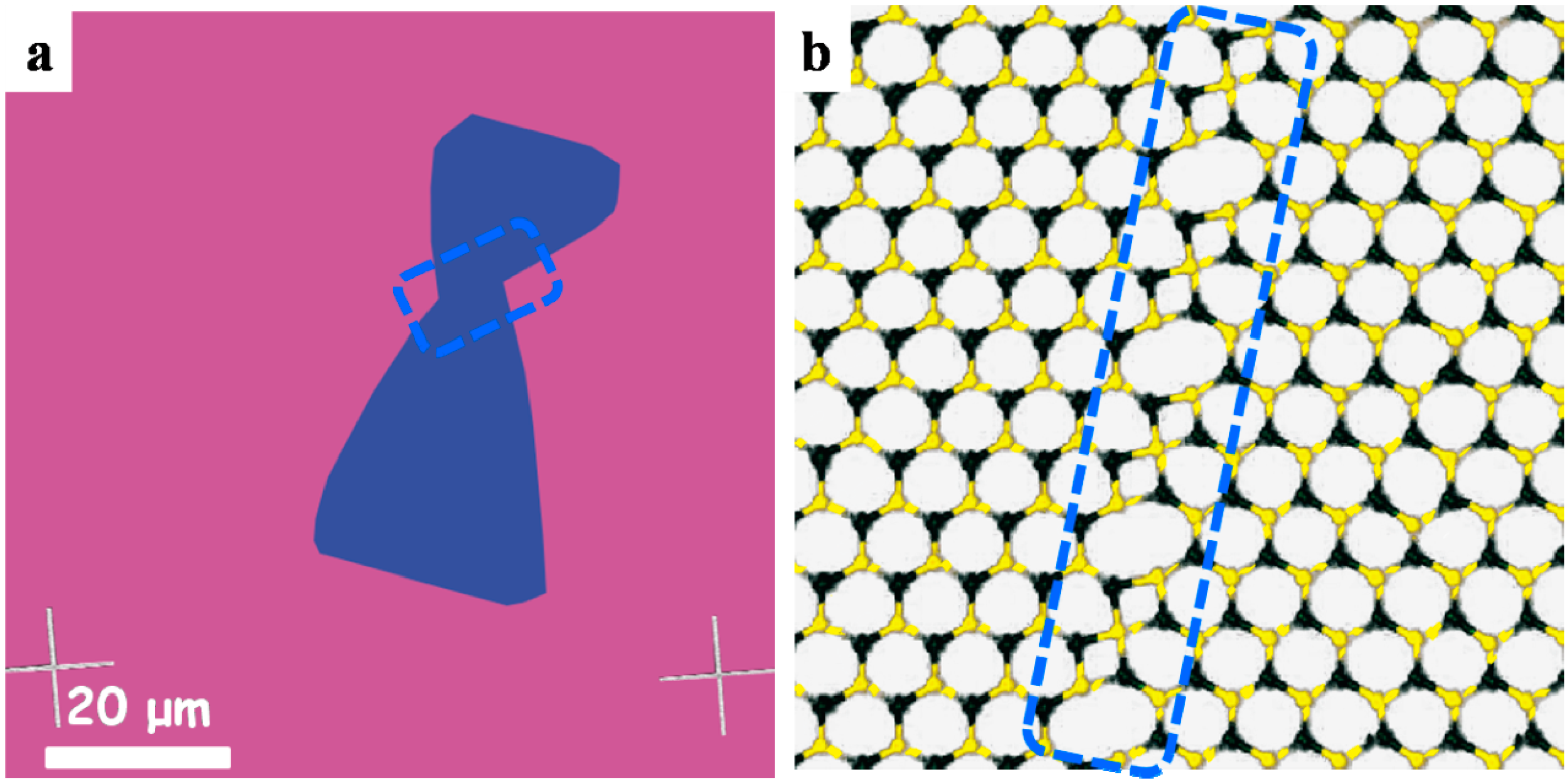
2.1. MoS2 with Twin GB Synthesis and the Atomistic Model

Monolayer MoS2 with twin GB was gown via van der Waals epitaxy on sapphire through low pressure oxygen-assisted CVD [19] (see Section 3.1) and then transferred from sapphire onto a SiO2 (300 nm thick)/Si substrate by wet chemical etching (see Section 3.2). There are only two lattice orientations for MoS2 (0° and 180°) due to the epitaxial growth mechanism, and two types of grain boundaries (0° grain boundary and twin grain boundary). Figure 1a shows the optical images of monolayer MoS2 transferred on a SiO2/Si substrate with increased contrast. Two grains were rotated 180° from one another and merged during the growth to form the twin GB. The optical images of other monolayer MoS2 with twin grain boundary and 0° grain boundary can be seen in supporting information (refer to Figure S1 and Figure S4). Figure 1b exhibits the atomistic model of the MoS2 and the twin GB with a recurring periodic 4-4-8 ring pattern [15].

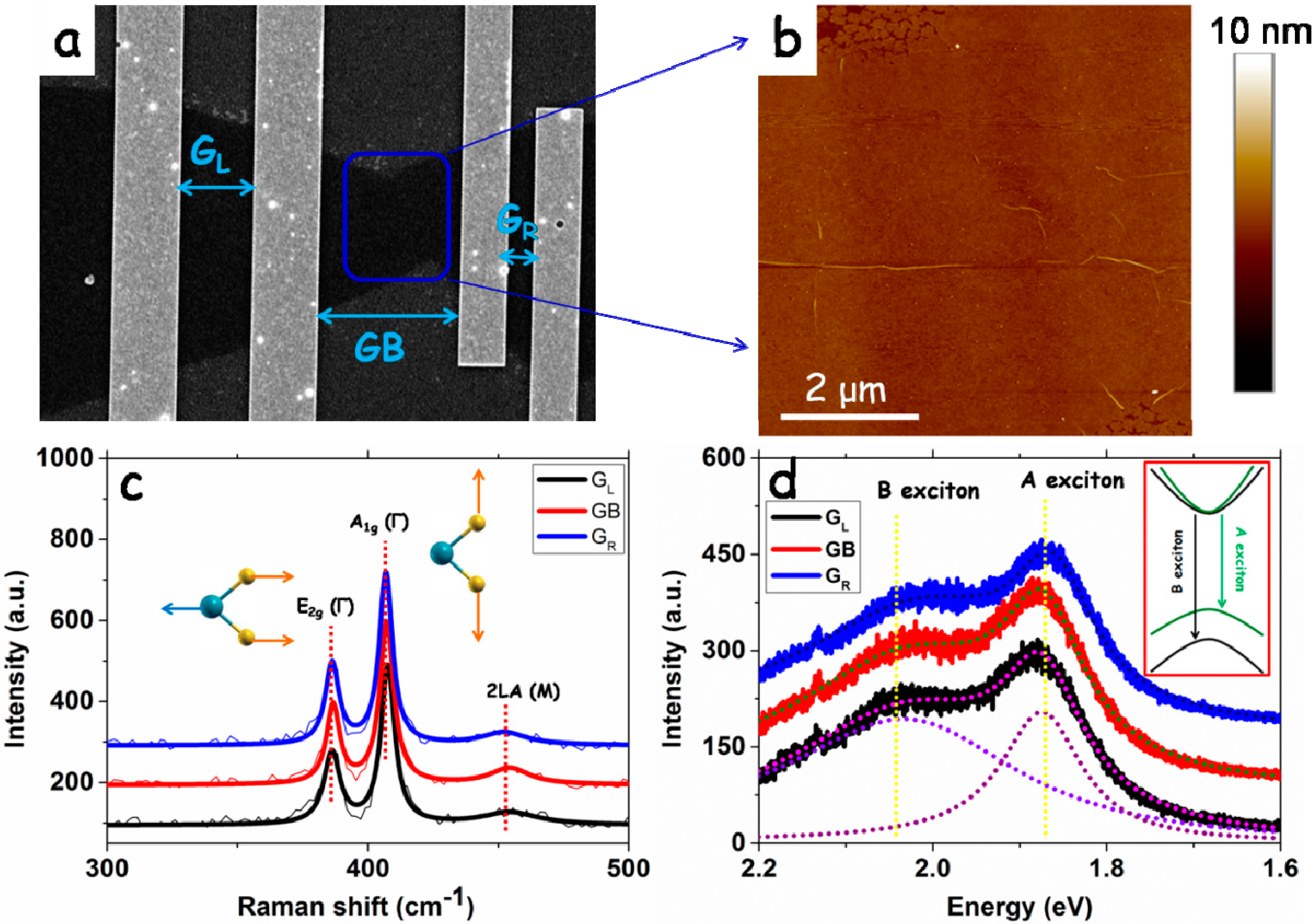
2.2. Device Fabrication and Spectroscopic Properties

Figure 2a shows the scanning electron microscopy (SEM) image of a typical device with multi-terminal electrodes on merged MoS2 grains with twin GB that allows us to measure intra-grain (within grain) and inter-grain (across twin GB) electrical properties. Figure 2b exhibits the atomic force microscopy (AFM) image of region shown in Figure 2a and reveals that the surface of sample is uniform without cracks and residues, except a few wrinkles caused by the transfer process and device fabrication. Figure 2c, Raman spectra excited by a 532 nm laser line, were collected and show no difference in the different regions of Figure 2a. Two main typical Raman active modes were found: E2g (Γ) at 386.3 cm−1 and A1g (Γ) at 405.6 cm−1 correspond to in-plane vibration of Mo and S atoms and out-of-plane vibration of the S atom respectively. Spacing between the two peaks (19.3 cm−1) confirms the monolayer nature [20,21]. At the same time, a broad peak at ~460 cm−1 assigned to the second-order zone-edge phonon peak 2LA(M) was observed [20]. The photoluminescence (PL) spectrum (Figure 2d) which keeps unchanged in the whole region shows two characteristic peaks at 1.87 eV (A excitation, derived from the direct band gap) and 2.03 eV (B excitation, originating from the valence band splitting of 160 meV caused by strong spin-obit coupling) [22,23]. Raman and PL spectra confirm the homogeneity of our sample for the subsequent transport properties measurement.

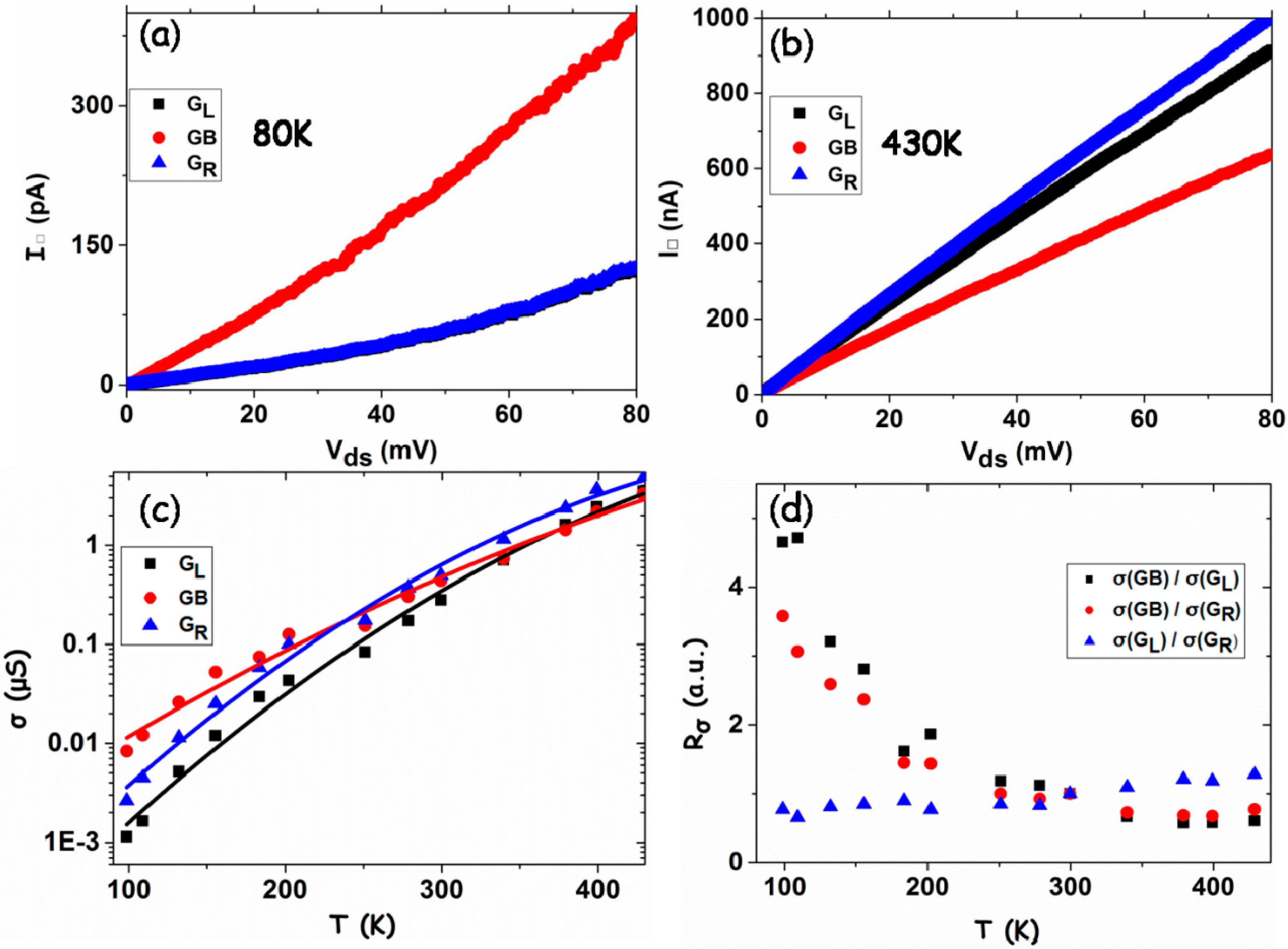
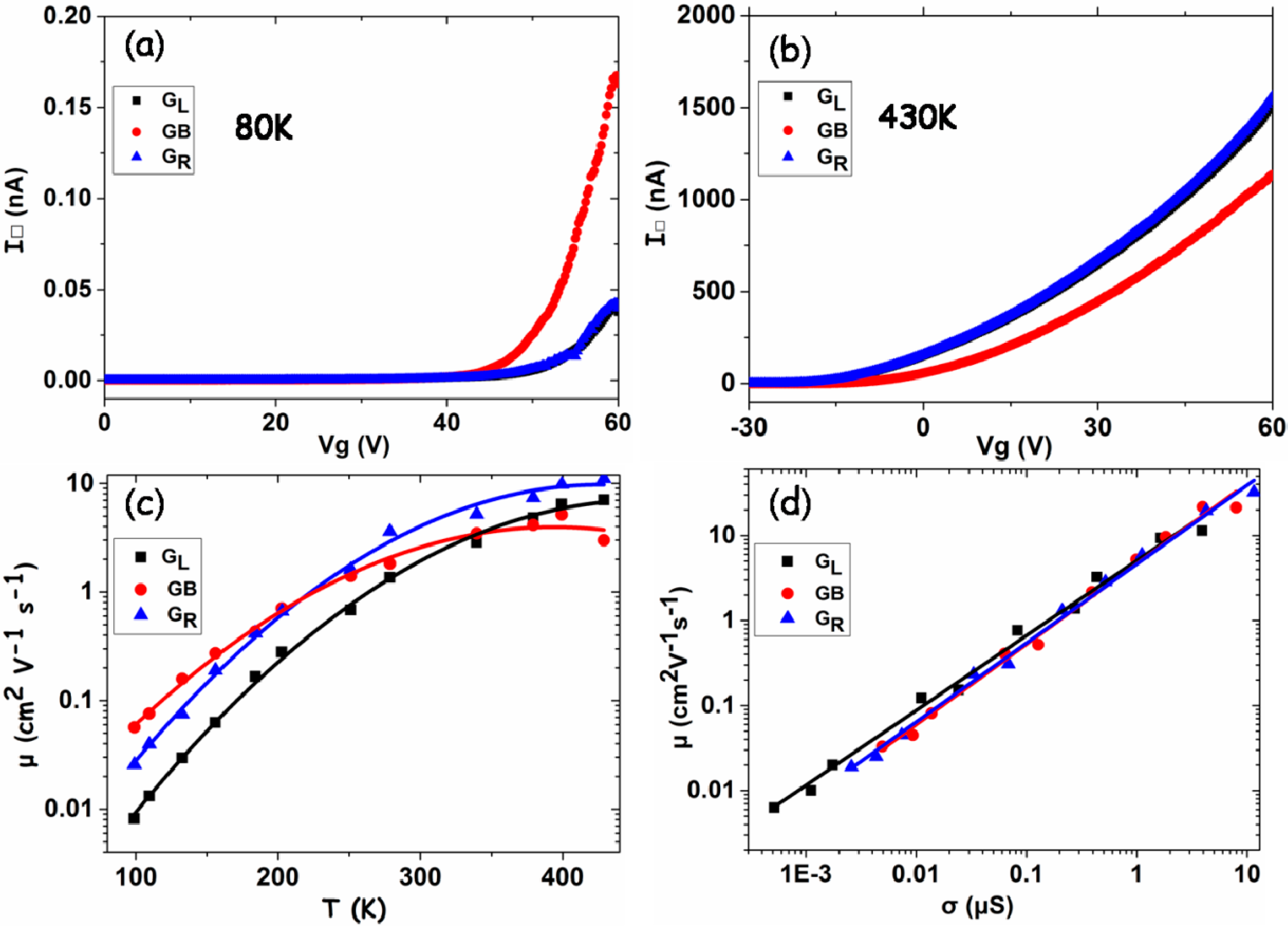
2.3. Transport Measurement

We have measured the transport characteristics of three samples with twin grain boundary (marked as sample 1, 2, and 3) and one sample with 0° grain boundary for intra-grain (GL and GR) , cross-grain boundary (GB), and along-grain boundary (G//) from 80 K to 430 K (the results of sample 2, 3, and 0° grain boundary are shown in supporting information). Taking into account the device geometry, we can extract the normalized effective current I□:
I =   I 0 L L W ( x )   d x
where I is current that we measured, L and W(x) is the sample length and width that varies along the direction of current. Figure 3a and Figure 4a are the output and transfer characteristics at 80 K, respectively, and show that the conductance across the twin grain boundary is larger than that in individual grains (left or right grain) at different carrier densities tuned by the back-gate voltage. While the normalized effective current of twin GB at 430 K is found to be less than that of each individual grain at various gate voltage showed in Figure 3b and Figure 4b. The output and transfer characteristics at different temperatures indicate that the device shows typical n-type behavior, and linear I−V curves demonstrate ohmic-like contact. Figure 3c,d exhibit the temperature dependence of electrical conductivity (σ) and relative conductivity (Rσ), and show that the conductance of twin GB is higher at lower temperature, but lower at higher temperature than that of individual grains. The relative conductivity between the left grain and right grain does not change with temperature and is almost equal to 1. While the relative conductivity between twin GB and individual grain increases dramatically with decreasing temperature and the conductivity for twin GB is four times of that for individual grains at 80 K. The transverse transports across the twin GB of samples 2 and 3 also show the analogous characteristics (refer to Figures S2 and S3). While 0° grain boundary has little effect on the transport (refer to Figure S4). These experimental results indicate that the transport mechanism of carrier in twin GB is different with the temperature changing. We will elucidate the reason later. The field-effect mobility (μ) is calculated from I□–Vg curves according to the following equation [24,25]:
μ   =   dI dV g 1 C ox V D
where Vg is the gate voltage, Cox is area-normalized capacitance of 300 nm thick SiO2 (11 nF/cm2), VD is the drain voltage, and the field-effect mobility is plotted as a function of temperature in Figure 4c. The trend of field-effect mobility with temperature is as the same as conductance. There is a universal relation between conductivity and mobility (shown in Figure 4d):
μ = σm
where m = 0.92, 0.94, 0.9 for GL, GB, GR, respectively. The relation can be explained by invoking a dense distribution of trap states, which acted as an impurity band and might come from the trapped charges in the substrate [26,27] or sulfur vacancies of MoS2 [28].

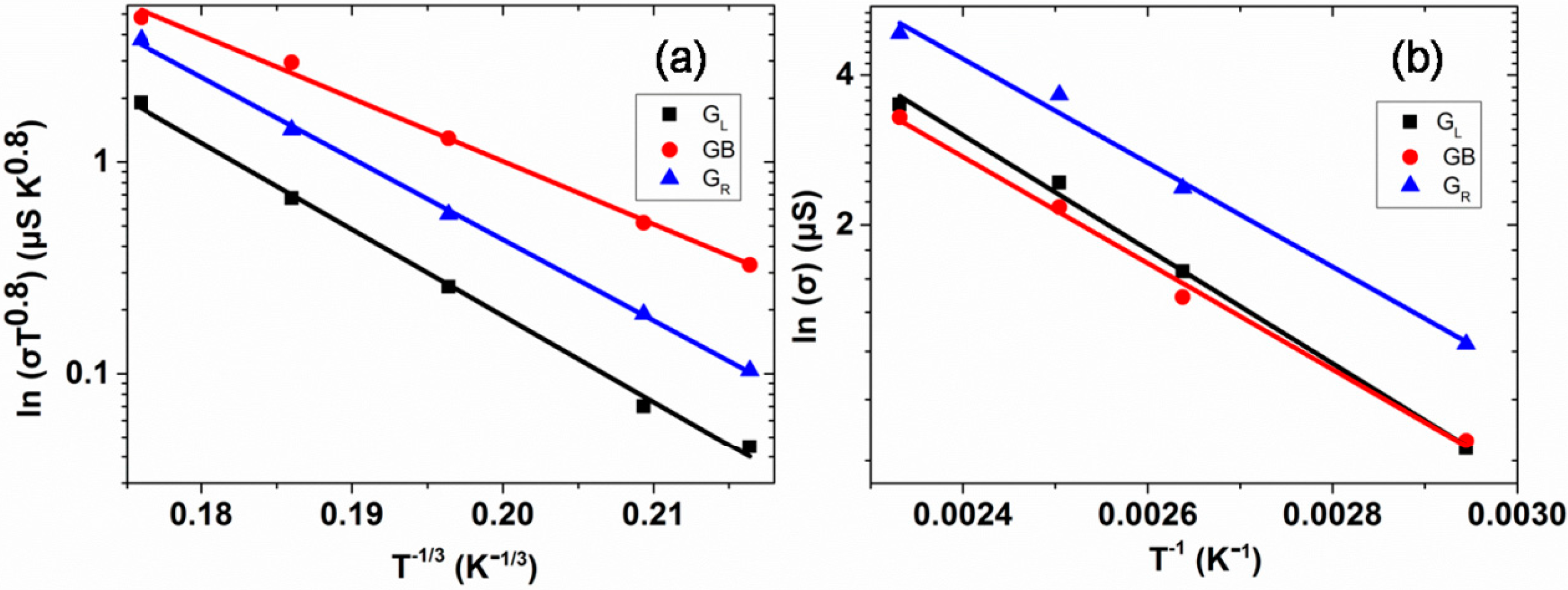
2.4. Transport Mechanism

We examine the temperature-dependent transport behavior in MoS2 with twin GB. The results summarized in Figure 5a,b can be used to identify the nature of the electronic states and the role of twin GB. It is evident from the temperature dependency of conductivity that the transport is dominated by a variable-range hopping (VRH) mechanism rather than thermally-activated behavior at low temperatures. Conductivity could be fitted very well by the 2D Mott VRH model given by:
σ = σ 0 ( T ) exp   [ ( T 0 T ) 1 / ( d + 1 ) ]
where T0 is the correlation energy scale, d is the dimensionality and equals 2 due to the monolayer scenario, and σ0(T) is a temperature-dependent conductivity prefactor with σ0(T) = ATm, where A is constant and m ~ 0.8–1, chosen as 0.8 in our analysis [26,29]. The observed behavior is common in highly-disordered systems and a signature of hopping transport via localized states [29,30,31]. The VRH transport is found to be consistent with the larger electrical conductivity of GB, due to localized mid-gap states that arises from twin GB can increase the hopping bond and conductivity [15,16,32,33]. The conductivity versus the inverse of temperature ( 1 T ) is exhibited in Figure 5b at high temperature, showing that the conductivity can be described by NNH transport with Arrhenius-type activated behavior:
σ = σ 0 exp   ( E a k B T )
where σ0 is a fitting parameter, Ea is the activation energy, and kB is Boltzmann constant [34,35]. In contrast with the VRH transport at low temperature, the NNH model at high temperature is reasonable for impeding the electrical transport by twin GB which serves as the line defects, scattering centers for charge carriers that can decrease the conductivity.

3. Materials and Methods

3.1. MoS2 with Twin GB Synthesis

Monolayer MoS2 was grown on sapphire by the oxygen-assisted chemical vapor deposition method in a three-temperature-zone furnace using MoO3 (Alfa Aesar, Shanghai, China, 99.999%) and S (Alfa Aesar, Shanghai, China, 99.9%) powder as precursors. Sulfur (in zone-I) and MoO3 powder (in zone-II) were separately loaded into two mini quartz tubes. Each of the three temperature zone was heated to preset values at a rate of 25 °C/min. And the temperatures of sulfur, MoO3, and the substrate are kept at 115, 530, and 850 °C, respectively, during growth.

3.2. MoS2 Transfer by Wet Chemical Etching

MoS2 on sapphire was firstly spin-coated by PMMA (950 K, 5% in anisole) at 3000 rpm for 60 s, and baked at 180° for 90 s. MoS2 with the PMMA coating was then soaked in 80° 2 mol/L KOH solution for 2.5 h to separate the PMMA/MoS2 films from the sapphire substrates. After several times of DI water rinsing, these films were received by SiO2/Si substrates. Acetone was used to dissolve the PMMA and MoS2 was annealed at 300° with 150 sccm Ar and 10 sccm H2.

3.3. Device Fabrication

The global back-gated MoS2 FET devices with twin GB were fabricated by e-beam lithography, e-beam evaporation of Ti (8 nm)/Au (30 nm) contact electrodes and lifting-off processes. Devices were annealed at 300° in 150 sccm Ar and 10 sccm H2 flow for 2h before electrical measurements.

3.4. Structure Characterizations

The morphology was characterized by AFM (MultiMode IIId, Veeco Instruments, New York, NY, USA) using tapping mode at room temperature in ambient atmosphere. The Raman and PL spectra were performed at room temperature on a Horiba Jobin Yvon LabRAM HR-Evolution Raman microscope (Paris, France ) with an excitation laser wavelength of 532 nm, laser power of 10 mW, and laser spot size of ~1 μm.

3.5. Transport Measurements

The output and transfer characteristics were measured from 80 K to 430 K in a close-cycle cryogenic probe station with a base pressure of 10−7 Torr.

4. Conclusions

The influence of twin GB on charge carriers of MoS2 has been investigated by transport studies at different temperatures. The twin GB plays different roles in affecting the electrical conductivity of MoS2 at different temperature ranges: dedicating localized mid-gap states at low temperature and the scattering center for carriers at high temperature. In the low-temperature region, the transport exhibits VRH, scattering for carriers can be ignored and twin GB can enhance the conductivity by dedicating localized mid-gap states and increasing the hopping path. While at high temperature, the transport shows NNH and the primary role of twin GB is the scattering center, which impedes the electrical transport. The temperature-dependent transport properties measurement provides a comprehensive illustration of the charge carrier transport mechanism in twin GB. The changed role of twin GB at different temperature ranges can help us design MoS2 electrical devices and tailor the electronic transport properties of MoS2 monolayers.

Supplementary Materials

The following are available online at https://www.mdpi.com/2073-4352/6/9/115/s1, Figure S1: Optical reflection images of samples 2 and 3, Figure S2: Sample 2 with twin grain boundary and transport measurement, Figure S3: Sample 3 with twin grain boundary and transport measurement, Figure S4: Sample with 0° grain boundary and transport measurement.

Acknowledgments

This work was supported by the National Natural Science Foundation of China (NSFC) under the grant No. 61325021.

Author Contributions

Luojun Du and Guangyu Zhang conceived and designed the experiments; Luojun Du performed the experiments; Luojun Du, Shuang Wu, Jing Zhao, Jing Zhang, Rong Yang analyzed the data; Hua Yu, Li Xie, Shuopei Wang, Xiaobo Lu, Jianling Meng, Jianqi Zhu, Peng Chen, Guole Wang contributed reagents/materials/analysis tools; Mengzhou Liao drew the atomistic model; Luojun Du and Dongxia Shi wrote the paper.

Conflicts of Interest

The authors declare no conflict of interest.

References

  1. Yu, Q.; Jauregui, L.A.; Wu, W.; Colby, R.; Tian, J.; Su, Z.; Cao, H.; Liu, Z.; Pandey, D.; Wei, D.; et al. Control and characterization of individual grains and grain boundaries in graphene grown by chemical vapour deposition. Nat. Mater. 2011, 10, 443–449. [Google Scholar] [CrossRef] [PubMed]
  2. Jauregui, L.A.; Cao, H.; Wu, W.; Yu, Q.; Chen, Y.P. Electronic properties of grains and grain boundaries in graphene grown by chemical vapor deposition. Solid State Commun. 2011, 151, 1100–1104. [Google Scholar] [CrossRef]
  3. Lu, L.; Shen, Y.; Chen, X.; Qian, L.; Lu, K. Ultrahigh Strength and High Electrical Conductivity in Copper. Science 2004, 304, 422–426. [Google Scholar] [CrossRef] [PubMed]
  4. Mak, K.F.; He, K.; Shan, J.; Heinz, T.F. Control of valley polarization in monolayer MoS2 by optical helicity. Nat. Nanotechnol. 2012, 7, 494–498. [Google Scholar] [CrossRef] [PubMed]
  5. Zeng, H.; Dai, J.; Yao, W.; Xiao, D.; Cui, X. Valley polarization in MoS2 monolayers by optical pumping. Nat. Nanotechnol. 2012, 7, 490–493. [Google Scholar] [CrossRef] [PubMed]
  6. Cao, T.; Wang, G.; Han, W.; Ye, H.; Zhu, C.; Shi, J.; Niu, Q.; Tan, P.; Wang, E.; Liu, B.; et al. Valley-selective circular dichroism of monolayer molybdenum disulphide. Nat. Commun. 2012, 3, 887–891. [Google Scholar] [CrossRef] [PubMed]
  7. Mak, K.F.; McGill, K.L.; Park, J.; Paul, L.; McEuen, P.L. The valley Hall effect in MoS2 transistors. Science 2014, 344, 1489–1492. [Google Scholar] [CrossRef] [PubMed]
  8. Lee, J.; Mak, K.F.; Shan, J. Electrical control of the valley Hall effect in bilayer MoS2 transistors. Nat. Nanotechnol. 2016, 11, 421–425. [Google Scholar] [CrossRef] [PubMed]
  9. Ye, J.T.; Zhang, Y.J.; Akashi, R.; Bahramy, M.S.; Arita, R.; Iwasa, Y. Superconducting dome in a gate-tuned band insulator. Science 2012, 338, 1193–1196. [Google Scholar] [CrossRef] [PubMed]
  10. Kohulák, O.; Martoňák, R.; Tosatti, E. High-pressure structure, decomposition, and superconductivity of MoS2. Phys. Rev. B 2015, 91, 144113. [Google Scholar] [CrossRef]
  11. Costanzo, D.; Jo, S.; Berger, H.; Morpurgo, A.F. Gate-induced superconductivity in atomically thin MoS2 crystals. Nat. Nanotechnol. 2016, 11, 339–344. [Google Scholar] [CrossRef] [PubMed]
  12. Radisavljevic, B.; Radenovic, A.; Brivio, J.; Giacometti, V.; Kis, A. Single-layer MoS2 transistors. Nat. Nanotechnol. 2011, 6, 147–150. [Google Scholar] [CrossRef] [PubMed]
  13. Liu, Y.; Wu, H.; Cheng, H.C.; Yang, S.; Zhu, E.; He, Q.; Ding, M.; Li, D.; Guo, J.; Weiss, N.O.; et al. Toward Barrier Free Contact to Molybdenum Disulfide Using Graphene Electrodes. Nano Lett. 2015, 15, 3030–3034. [Google Scholar] [CrossRef] [PubMed]
  14. Li, X.; Zhang, F.; Niu, Q. Unconventional quantum Hall effect and tunable spin Hall effect in Dirac materials: Application to an isolated MoS2 trilayer. Phys. Rev. Lett. 2013, 110, 066803. [Google Scholar] [CrossRef] [PubMed]
  15. Van der Zande, A.M.; Huang, P.Y.; Chenet, D.A.; Berkelbach, T.C.; You, Y.M.; Lee, G.H.; Heinz, T.F.; Reichman, D.R.; Muller, D.A.; Hone, J.C. Grains and grain boundaries in highly crystalline monolayer molybdenum disulphide. Nat. Mater. 2013, 12, 554–561. [Google Scholar] [CrossRef] [PubMed]
  16. Zou, X.; Liu, Y.; Yakobson, B.I. Predicting dislocations and grain boundaries in two-dimensional metal-disulfides from the first principles. Nano Lett. 2012, 13, 253–258. [Google Scholar] [CrossRef] [PubMed]
  17. Liu, H.; Jiao, L.; Yang, F.; Cai, Y.; Wu, X.; Ho, W.; Gao, C.; Jia, J.; Wang, N.; Fan, H.; et al. Dense network of one-dimensional midgap metallic modes in monolayer MoSe2 and their spatial undulations. Phys. Rev. Lett. 2014, 113, 066105. [Google Scholar] [CrossRef] [PubMed]
  18. Barja, S.; Wickenburg, S.; Liu, Z.F.; Zhang, Y.; Ryu, H.; Ugeda, M.M.; Hussain, Z.; Shen, Z.X.; Mo, S.K.; Wong, E.; et al. Charge density wave order in 1D mirror twin boundaries of single-layer MoSe2. Nat. Phys. 2016, 12, 751–756. [Google Scholar] [CrossRef]
  19. Chen, W.; Zhao, J.; Zhang, J.; Gu, L.; Yang, Z; Li, X.; Yu, H.; Zhu, X.; Yang, R.; Shi, D.; et al. Oxygen-Assisted Chemical Vapor Deposition Growth of Large Single-Crystal and High-Quality Monolayer MoS2. J. Am. Chem. Soc. 2015, 137, 15632–15635. [Google Scholar] [CrossRef] [PubMed]
  20. Li, H.; Zhang, Q.; Yap, C.C.R.; Tay, B.K.; Edwin, T.H.T.; Olivier, A.; Baillargeat, D. From bulk to monolayer MoS2: Evolution of Raman scattering. Adv. Funct. Mater. 2012, 22, 1385–1390. [Google Scholar] [CrossRef]
  21. Zhang, J.; Yu, H.; Chen, W.; Tian, X.; Liu, D.; Cheng, M.; Xie, G.; Yang, W.; Yang, R.; Bai, X.; et al. Scalable growth of high-quality polycrystalline MoS2 monolayers on SiO2 with tunable grain sizes. ACS Nano 2014, 8, 6024–6030. [Google Scholar] [CrossRef] [PubMed]
  22. Mak, K.F.; Lee, C.; Hone, J.; Shan, J.; Heinz, T.F. Atomically thin MoS2: A new direct-gap semiconductor. Phys. Rev. Lett. 2010, 105, 136805. [Google Scholar] [CrossRef] [PubMed]
  23. Zhu, Z.Y.; Cheng, Y.C.; Schwingenschlögl, U. Giant spin-orbit-induced spin splitting in two-dimensional transition-metal dichalcogenide semiconductors. Phys. Rev. B 2011, 84, 153402. [Google Scholar] [CrossRef]
  24. Schmidt, H.; Wang, S.; Chu, L.; Toh, M.; Kumar, R.; Zhao, W.; Neto, A.H.C.; Martin, J.; Adam, S.; Özyilmaz, B.; et al. Transport properties of monolayer MoS2 grown by chemical vapor deposition. Nano Lett. 2014, 14, 1909–1913. [Google Scholar] [CrossRef] [PubMed]
  25. Jariwala, D.; Sangwan, V.K.; Late, D.J.; Johns, J.E.; Dravid, V.P.; Marks, T.J.; Lauhon, L.J.; Hersam, M.C. Band-like transport in high mobility unencapsulated single-layer MoS2 transistors. Appl. Phys. Lett. 2013, 102, 173107. [Google Scholar] [CrossRef]
  26. Ghatak, S.; Pal, A.N.; Ghosh, A. Nature of electronic states in atomically thin MoS2 field-effect transistors. ACS Nano 2011, 5, 7707–7712. [Google Scholar] [CrossRef] [PubMed]
  27. Paasch, G.; Lindner, T.; Scheinert, S. Variable range hopping as possible origin of a universal relation between conductivity and mobility in disordered organic semiconductors. Synth. Met. 2002, 132, 97–104. [Google Scholar] [CrossRef]
  28. Qiu, H.; Xu, T.; Wang, Z.; Ren, W.; Nan, H.; Ni, Z.; Chen, Q.; Yuan, S.; Miao, F.; Song, F.; et al. Hopping transport through defect-induced localized states in molybdenum disulphide. Nat. Commun. 2013, 4, 2642–2647. [Google Scholar] [CrossRef] [PubMed]
  29. Mott, V.F.; Davis, E.A. Electronic Processes in Non-Crystalline Materials; Clarendon Press: Oxford, UK, 1971. [Google Scholar]
  30. Najmaei, S.; Amani, M.; Chin, M.L.; Liu, Z.; Birdwell, A.G.; O’Regan, T.P.; Ajayan, P.M.; Dubey, M.; Lou, J. Electrical transport properties of polycrystalline monolayer molybdenum disulfide. ACS Nano 2014, 8, 7930–7937. [Google Scholar] [CrossRef] [PubMed]
  31. Han, M.Y.; Brant, J.C.; Kim, P. Electron Transport in Disordered Graphene Nanoribbons. Phys. Rev. Lett. 2010, 104, 056801. [Google Scholar] [CrossRef] [PubMed]
  32. Zhou, W.; Zou, X.; Najmaei, S.; Liu, Z.; Shi, Y.; Kong, J.; Lou, J.; Ajayan, P.M.; Yakobson, B.I.; Idrobo, J.C. Intrinsic structural defects in monolayer molybdenum disulfide. Nano Lett. 2013, 13, 2615–2622. [Google Scholar] [CrossRef] [PubMed]
  33. Liu, X.; Balla, I.; Bergeron, H.; Hersam, M.C. Point Defects and Grain Boundaries in Rotationally Commensurate MoS2 on Epitaxial Graphene. J. Phys. Chem. C 2016. [Google Scholar] [CrossRef]
  34. Zhang, J.; Wang, J.; Chen, P.; Sun, Y.; Wu, S.; Jia, Z.; Lu, X.; Yu, H.; Chen, W.; Zhu, J.; et al. Observation of Strong Interlayer Coupling in MoS2/WS2 Heterostructures. Adv. Mater. 2016, 28, 1950–1956. [Google Scholar] [CrossRef] [PubMed]
  35. Zhu, W.; Low, T.; Lee, Y.H.; Wang, H.; Farmer, D.B.; Kong, J.; Xia, F.; Avouris, P. Electronic transport and device prospects of monolayer molybdenum disulphide grown by chemical vapour deposition. Nat. Commun. 2014, 5, 3087–3094. [Google Scholar] [CrossRef] [PubMed]
Figure 1. (a) Optical reflection image of MoS2 on a SiO2 (300 nm)/Si substrate. The image contrast has been increased for visibility; violet is the bare substrate, and blue represents monolayer MoS2. (b) An atomistic model of the MoS2 with twin GB. The black spots are Mo atoms; the yellow spots are two stacked S atoms. The region marked with blue frame line in (a) and (b) is the twin GB.
Crystals 06 00115 g001
Figure 2. (a) SEM image of a device with four electrodes contacting two coalesced MoS2 grains, GL, GB, and GR represent the left grain, grain boundary, and right grain; (b) AFM image of region shown in (a); (c) Raman spectra and atomic displacements of the typical Raman-active modes; and (d) PL spectra and the band structure shows the valence band splitting at the K point of the Brillouin zone; the dashed line is the Lorentz fitting.
Crystals 06 00115 g002
Figure 3. (a,b) Output characteristics at 80 K and 430 K, respectively; (c) temperature dependence of electrical conductivity σ; and (d) relative conductivity Rσ at different temperatures.
Crystals 06 00115 g003
Figure 4. (a,b) Transfer characteristics at 80 K and 430 K, respectively; (c) temperature dependence of mobility μ; and (d) the relation between mobility μ and conductivity σ.
Crystals 06 00115 g004
Figure 5. (a) Temperature dependence of conductivity and variable range hopping. The solid lines are the linear fit to the data that indicate VRH behavior at low temperature; and (b) temperature dependence of conductivity and nearest-neighbor hopping. The solid lines are the linear fit to the data and indicate NNH behavior at high temperature.
Crystals 06 00115 g005

