Review

Van Der Waals Heterostructures between Small Organic Molecules and Layered Substrates

1
Hunan Key Laboratory of Super-microstructure and Ultrafast Process, School of Physics and Electronics, Central South University, Changsha 410083, China
2
State Key Laboratory of Powder Metallurgy, Central South University, Changsha 410083, China
3
Department of Physics, National University of Singapore, 2 Science Drive 3, Singapore 117542, Singapore
4
Department of Physics and Astronomy, University of Rochester, Rochester, NY 14627, USA
*
Authors to whom correspondence should be addressed.
Crystals 2016, 6(9), 113; https://doi.org/10.3390/cryst6090113
Submission received: 16 July 2016 / Revised: 27 August 2016 / Accepted: 30 August 2016 / Published: 9 September 2016

Abstract

:
Two dimensional atomic crystals, like grapheme (G) and molybdenum disulfide (MoS2), exhibit great interest in electronic and optoelectronic applications. The excellent physical properties, such as transparency, semiconductivity, and flexibility, make them compatible with current organic electronics. Here, we review recent progress in the understanding of the interfaces of van der Waals (vdW) heterostructures between small organic molecules (pentacene, copper phthalocyanine (CuPc), perylene-3,4,9,10-tetracarboxylic dianhydride (PTCDA), and dioctylbenzothienobenzothiophene (C8-BTBT)) and layered substrates (G, MoS2 and hexagonal boron nitride (h-BN)). The influences of the underlying layered substrates on the molecular arrangement, electronic and vibrational properties will be addressed.

Graphical Abstract

1. Introduction

Organic (opto-)electronics are attracting tremendous attention for their mechanical flexibility, light weight, low cost, and available large scale production in organic light emitting diodes (OLEDs), organic photovoltaics (OPVs), and organic field effect transistors (OFETs) [1,2,3,4,5]. The quality of organic semiconductor thin films is one of the key components for a better device performance. Figure 1a–d shows the molecular structures of four air-stable candidates for organic electronics, pentacene, copper phthalocyanine (CuPc), perylene-3,4,9,10-tetracarboxylic dianhydride (PTCDA) and dioctylbenzothienobenzothiophene (C8-BTBT), respectively. The anisotropic structures suggest orientation-dependent electronic properties. For example, pentacene possesses a relatively higher mobility in its b-c plane than a-b plane, as shown in Figure 1e [6,7]. Thus, various substrates, metals [8,9,10], native oxide silica [11,12,13,14], and layered materials [6,7,15,16,17,18], have been chosen for the growth of high quality thin films. In order to optimize the devices performance, it is essential to clarify how the interactions between molecules and substrates affect the growth of organic thin films.
The two dimensional (2D) derivatives of layered materials, such as single- or few-layered (SL, FL) molybdenum disulfide (MoS2), hexagonal boron nitride (h-BN), and graphene (G), whose structures are schematically shown in Figure 1f and exhibiting an atomically flat surfaces without dangling bonds, are thought to be perfect candidates to fundamental researches and practical applications. G has the advantages such as very high charge carrier mobility, good flexibility, and transparency to be used as a transparent electrode substituting indium−tin oxide (ITO) [19,20]. h-BN is an insulating isomorph of G with covalent bonding boron and nitrogen atoms occupying the inequivalent positions, possessing a low dielectric constant. MoS2 is composed by one layer of Mo atoms stacked between two sulfide layers and used as channel materials in FETs because of its high on/off ratio, low sub-threshold swing value, and good carrier mobility [21,22,23,24]. G, MoS2, and h-BN are all chemically inert, avoiding bonding strongly when integrating with different dimensional crystals at the interface and leading to 2D-2D and 0D-2D (organic molecules-2D) van der Waals (vdW) heterostructures [25,26,27]. For example, MoS2-G vdW heterostructure shows that close to the Fermi level, no significant charge transfer doping is detected from MoS2 to G [28,29]. Besides, organic molecules are able to grow into well-ordered thin film with a high degree of crystallinity on 2D substrates and form vdW heterostructures. Such vdW heterostructures possess potential applications in FET devices [30]. Moreover, the excellent physical properties, such as transparency and flexibility, make them compatible with current organic (opto-)electronics.
This review consists of following six sections: I tuning the orientation of pentacene, II pentacene on layered substrates, III CuPc on layered substrates, IV C8-BTBT on layered substrates, V PTCDA on layered substrates, and VI conclusions.

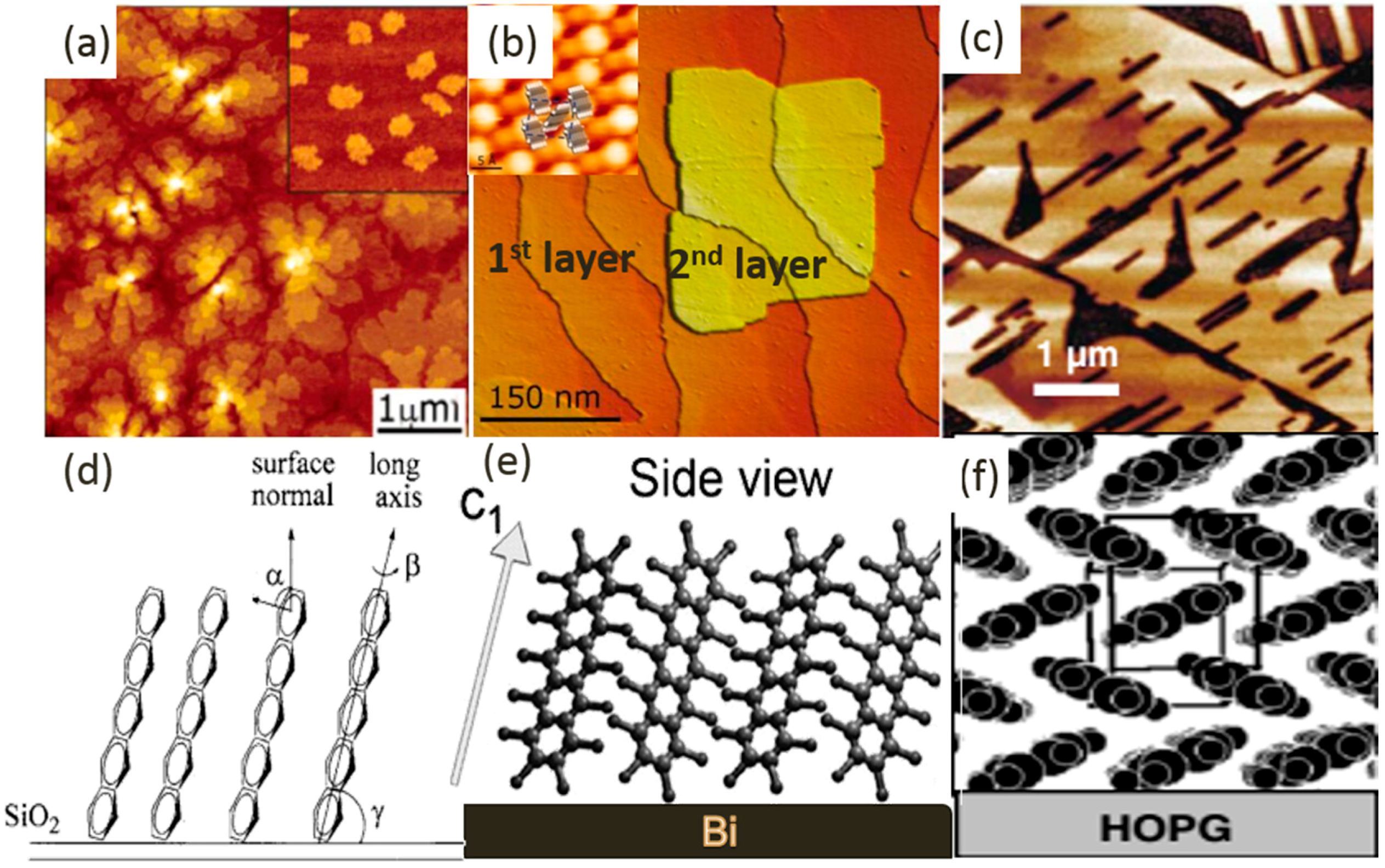
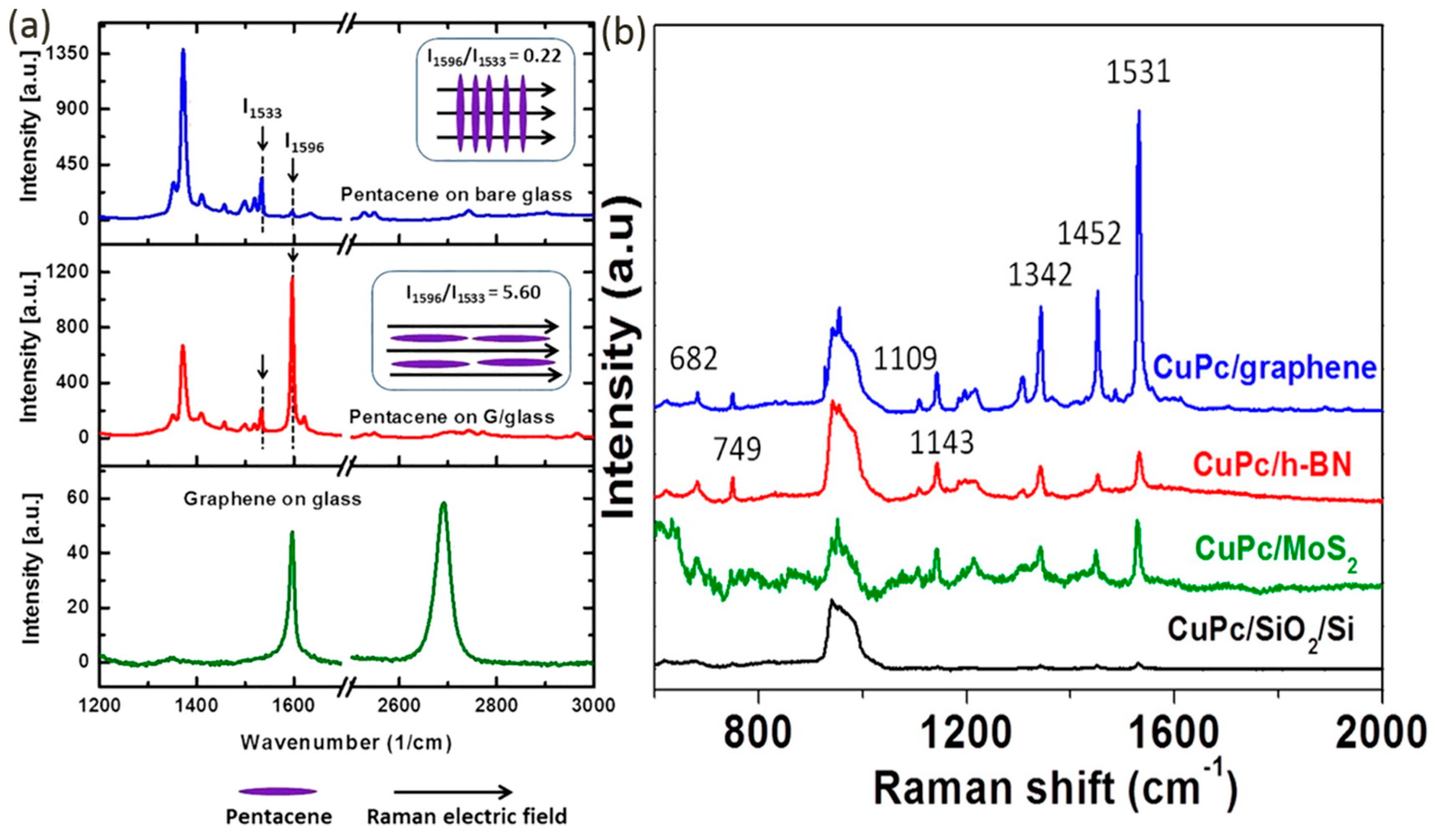
2. Tuning the Orientation of Pentacene

As a well-known gate dielectric, SiO2 is one of most usual substrates to study the properties of thin films of small organic molecules, for example, pentacene. The AFM image in Figure 2a shows the typical morphological features of ~3 ML (ML, monolayer, a full layer of molecules in the standing-up configuration) pentacene thin films on SiO2 [12]. Such films are composed by dendritic grains with flat surfaces and well-ordered crystalline structures in size of few micrometers, indicating a kinetics-limited Volmer-Weber growth mode [31,32]. The corresponding inset shows the nucleation and extension of pentacene in the first monolayer into dendritic grains, indicating presence of plenty of grain boundaries in thicker films. The average step height of ~1.5 nm, close to the length of one pentacene molecule, suggests that pentacene molecules always stand up on SiO2 (molecular a-b plane parallel to the substrate surface) as shown in Figure 2d, which can be attributed to the relatively weak interfacial interaction between pentacene and SiO2. Consequently, the charge carriers in such pentacene thin films prefer to lateral transport along the overlapped π orbitals with high mobilities up to 5 cm2/Vs [33]. However, the existed plenty of grain boundaries may scatter the charge carriers and reduce the mobilities. Given that molecule-substrate and molecule-molecule interactions predominantly determine the film structures, so as to enhance the device’s performance, an adequate substrate is urgently required to ensure higher-crystalline pentacene thin films.
STM image in Figure 2b shows that Bi(001) is covered by an ordered single layer pentacene entirely and a second layer partially (with brighter contrast) [8]. The pentacene layer grows in a step flow mode, like h-BN grown on Ru(0001) [34], which can effectively reduce the grain boundaries and result the first layer pentacene in grains with a larger size exceeding 200 μm in diameter. The inserted molecularly-resolved STM image shows aligned spots. Each of them corresponds to a single standing-up pentacene molecule, indicating the pentacene molecular a-b plane parallel to Bi(001), as show in Figure 2e. Angle Resolved Photoemission Spectroscopy (ARPES) measurements demonstrate a higher highest occupied molecular orbital (HOMO) dispersion and more delocalized charge carriers than theoretical calculations along three high symmetrical directions ( Γ ¯ M ¯ , Γ ¯ Y ¯ and Γ ¯ X ¯ ), which means a larger overlap of π-orbitals and higher carrier mobilties [9]. The results indicate the Bi(001) indeed improved the crystallinity of pentacene films and induced higher mobility.
HOPG is a famous inert substrate for surface science researches. The AFM image in Figure 2c shows the morphology of ~12 nm thick pentacene films on HOPG, which is characterized by large block-like ordered crystals with deep trenches [6]. On the contrary to above two cases, the long axes of pentacene molecules are parallel to the substrate surface according to X-ray diffraction results. Such a lying-down arrangement, as schematically shown in Figure 2f, can be attributed to the improved interfacial π-π interactions due to the epitaxial growth of pentacene on HOPG. The rather weak adsorption energy of the molecules on graphite enables a slight tilting of the molecules at the interface and thus allows the formation of crystalline multilayer films by suppressing any strain due to lattice mismatch between the molecular film and the substrate [35]. The films are possibly in orthorhombic polymorph and possess fiber textures with (100) as the fiber long axis along the surface normal. Thus, they have high enough crystallinity to show a HOMO-derived band dispersion of ~190 meV at room temperature, which is absent for pentacene grown on SiO2 [6]. The results indicate that layered substrates like HOPG and MoS2, moreover, their single- or few- layered derivatives like G and MoS2, may improve the crystallinity of thin films of small organic molecules.

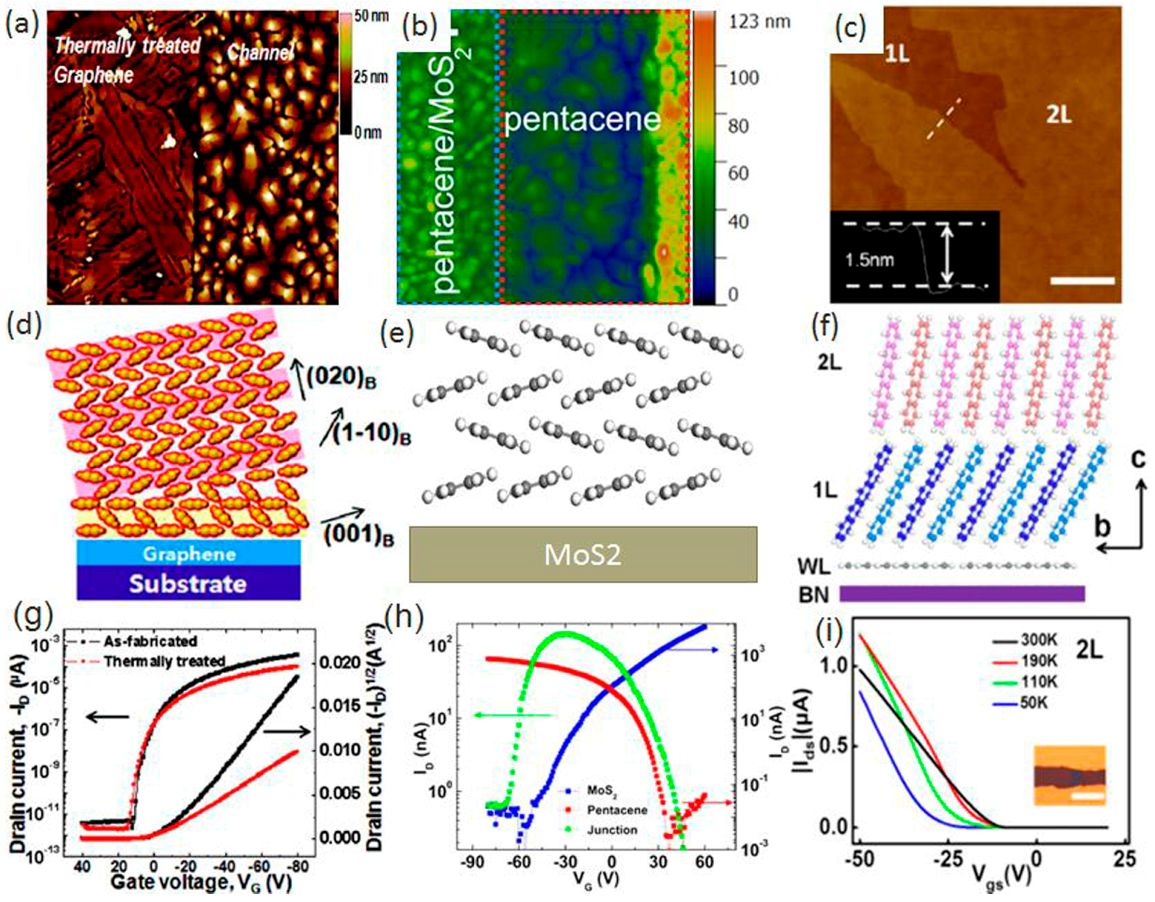
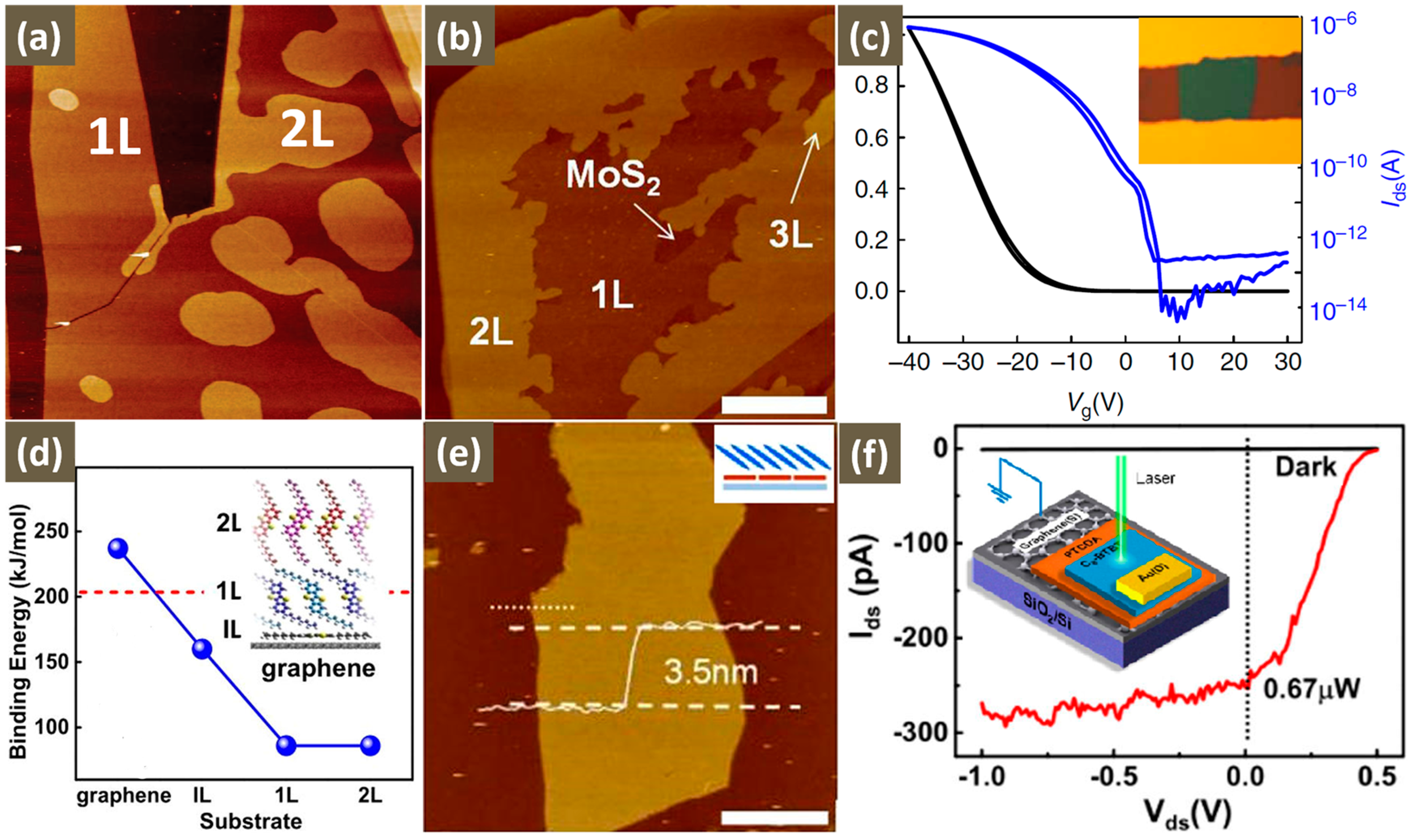
3. Pentacene on Layered Substrates

In terms of devices, G is an ideal electrode material due to its outstanding conductivity, flexibility, and transparency. Conductive and transparent monolayer G can be used as a template to tune pentacene molecular orientation from standing-up to lying-down in well-defined films [15,36]. The AFM image in Figure 3a shows that the morphology of 50 nm thick pentacene films on CVD-G-covered and bare SiO2 has an abrupt change cross the boundary, which revealed remarkable differences in growth and the modulation effect of substrates. Pentacene films on G (left-hand side) show a highly ordered block-like crystals with deep trenches texture, similar to on HOPG, while on SiO2 (right-hand side) are in typical polycrystalline grains [15]. They differ greatly in crystallinity, grain size, and orientation. Both the angle-dependent near-edge X-ray absorption fine structure (NEXAFS) and two-dimensional grazing incidence X-Ray diffraction (2D GIXRD) measurements corroborate that pentacene molecules in the first layer are in a lying-down orientation, while slightly tilted relative to the G plane in subsequent layers, as depicted in Figure 3d. It is ascribed to that the interfacial π-π interaction is reduced when pentacene grows into several layers [15]. It is well adapted to the cases of pentacene on G-covered glass [36] and perfluoropentacene on G-covered quartz [37]. It’s also important to mention that polymer residues remaining on G surfaces induce a stand-up orientation of pentacene [15]. The Fe film morphology was influenced by substrate surface defects [38]. Considering this reason, there can be a distinct structure and orientation of pentacene film if the substrate surface exhibits defects or becomes rough, because the template effect is no longer operative. In that case, molecules adsorb in an upright orientation and continue to grow as (001) oriented films. Thus, it is a crucial factor which avoids surface defects and roughness when utilizing template-guided molecular film growth [35]. The particular interaction between G and small molecules [39] is used to govern both the thin film morphology and electronic characteristics of pentacene films.
The AFM image in Figure 3b displays the morphology of 40 nm thick pentacene on SiO2 covered with/without mechanically exfoliated 2L MoS2 (blue/red dash block) [40]. On the MoS2 side, pentacene, perhaps in a lying-down configuration (Figure 3e), is more compact and homogeneous but in smaller grains. The abrupt change in the pentacene film grain size coincides with the boundary with the underlying MoS2.
The AFM image in Figure 3c shows the well-defined crystal facets of ~2 ML pentacene grown on mechanically-exfoliated h-BN [7], indicating that pentacene is highly-crystalline and grows in a layer-by-layer mode with obvious difference in the first three layers. The average thickness of the wetting layer (WL), the first (1L), and the second conducting layer (2L) are 0.5, 1.14, and 1.58 nm, respectively. The subsequent layers have the same height and molecular packing as 2L. The thickness of WL approximates the length of pentacene molecule along b-axis (0.606 nm), and far less than that along c-axis (1.601 nm) [12], which indicates the molecules adopt the lying-down configuration. In addition, the thickness of 2L is consistent with the (001) plane spacing of thin film phase (1.45 nm). However, 1L is clearly in a new polymorph which slightly differs with 2L. The transitional height implies more tilted molecular packing compared to 2L, as schematically illustrated in Figure 3f. The molecular packing is very different with on G and MoS2.
Figure 3g–i shows the transfer characteristics of pentacene based OFETs with G, MoS2 and h-BN as function layers, respectively. Figure 3g demonstrates transfer characteristics of lateral FETs using monolayer G with/without PMMA residues (black/red curve) as electrodes. The devices with/without PMMA residues show an average field-effect mobility of 1.2/0.4 cm2/Vs and a comparable current on-off ratio of 108. The poorer field-effect mobility is due to the orientation of the pentacene long axis parallel to the substrate plane on clean G. That is, the π conjugate direction is normal to electron transport direction of planar FET devices.
Figure 3h displays the transfer characteristics of a MoS2 FET (blue), a pentacene FET (red), and a type II p-n heterojunction based on pentacene/MoS2 (green), respectively [40]. The gate-tunable asymmetric antiambipolar transfer characteristic of pentacene/MoS2 heterojuntion is different than the symmetric one with a MoS2−WSe2 p-n heterojunctions [41,42], suggesting harnessing to achieve simultaneous phase [43] and amplitude [44] shift-keying for wireless telecommunication technologies. In addition, this heterojunction exhibits a photovoltaic effect but poor power conversion efficiencies of ~0.004% @ 625 nm, Performance of FET devices is unsatisfied because of a low on/off ratio and mobility. It seems that the reduced carrier diffusion length results from charge carrier scattering and trapping due to smaller grain size. Hence, the crystalline of pentacene on MoS2 continue to be a primary issue for application.
Figure 3i shows the temperature dependent transfer characteristics of a 2L pentacene/h-BN based FET [7]. The extracted field effect mobility is about 3 and 5.2 cm2/Vs at room- and low-temperature (110 K), respectively, far surpassing devices based on pentacene polycrystalline thin films at similar temperatures. On the contrary to the bandlike transport of 2L devices, the WL devices exhibit no conduction due to the absence of intralayer π-π stacking, and the 1L devices display characteristic of 2D hopping transport mode. In 2L, a sufficient extended density of states along a-b plane caused by the π orbital laterally-overlapping leads to bandlike transport for planar FETs. In 1L, a more tilted molecular orientation results in disconnected bonding and localization in both directions. The strong modulation demonstrates that h-BN is an excellent candidate for an insert layer which enables the conversion of molecules’ arrangement by vdW interactions.

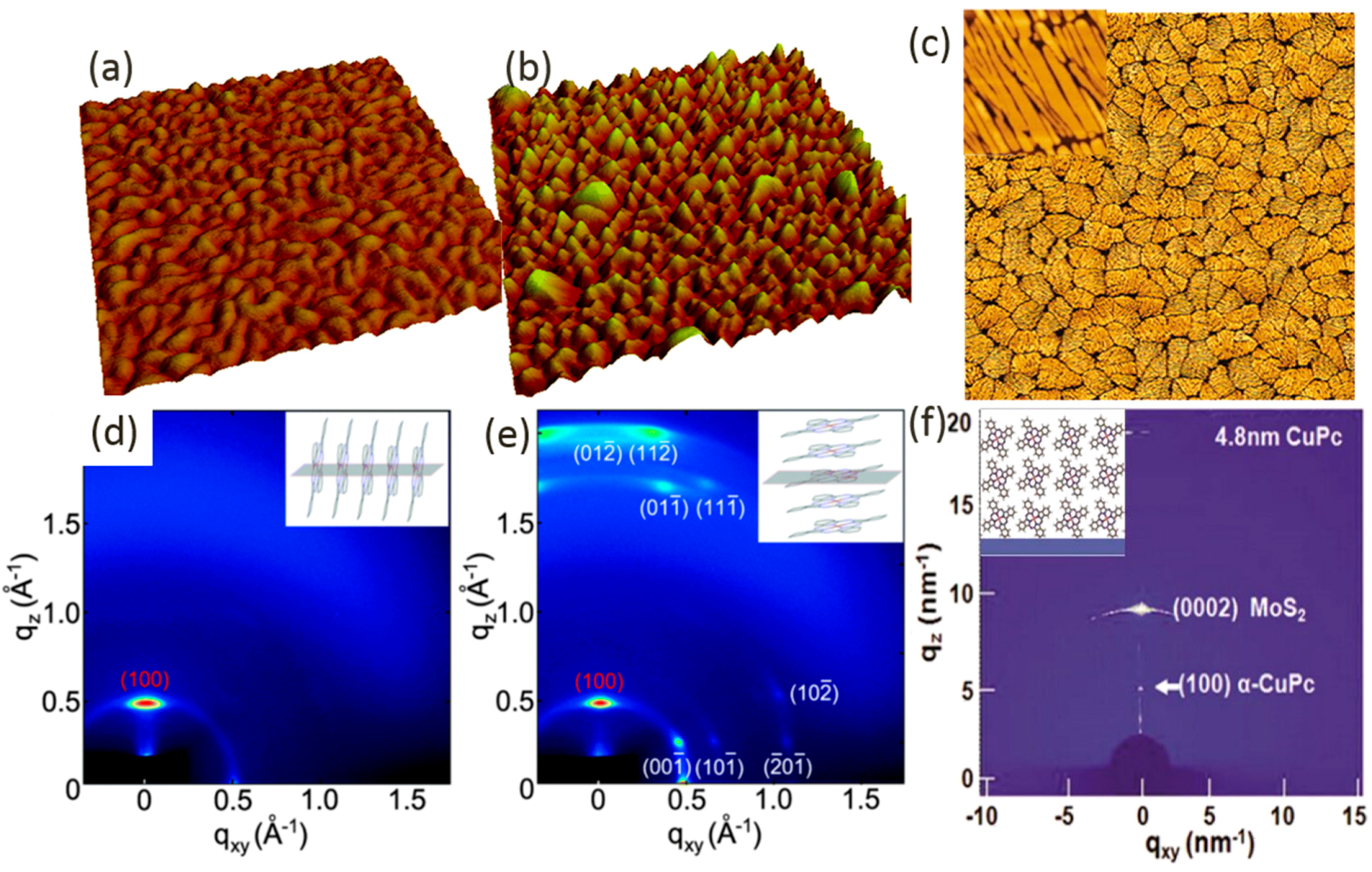
4. CuPc on Layered Substrates

The modulation of layered substrates on the growth of CuPc are also interesting. Figure 4a,b show the AFM topography images CuPc on glass covered with/without CVD-grown G [45]. On bare glass, elongated CuPc grains, 94 ± 34 nm long and 35 ± 6 nm wide, are observed with a root mean squared film roughness of 2.0 nm, and similar to previous AFM observations of standing up oriented CuPc [46,47].Round CuPc grains are observed on a few layers of G (FLG) with a greater roughness of 4.2 nm. The 2D-GIXRD pattern in Figure 4d for CuPc on bare glass only shows one single sharp peak concentrated on the meridian (qxy = 0), implying that CuPc molecules are oriented perpendicularly to the surface of the glass substrate, similarly on Si [48]. On the contrary, the pattern in Figure 4e shows multiple new diffraction points for CuPc on FLG-covered glass. Furthermore, it is not dispersed much, indicating that CuPc molecules are well oriented on G-covered glass [49]. Thus, CuPc adopts a near face-on orientation with the molecular plane tilted on average 9° with respect to the substrate. The continued appearance of the (100) reflection along the meridian indicates that there are still some crystallites adopt the edge-on configuration in the film [48]. Conductive atomic force microscopy (C-AFM) measurements show that at a single-grain level CuPc on (G covered) PEDOT:PSS/ITO presents a hole mobility of (1.9 ± 0.2) × 10−3 ((1.6 ± 0.2) × 10−2) cm2/Vs. G-templated CuPc thin films exhibit an order of magnitude higher out-of plane hole mobility relative to untemplated thin films. Whether the G coating affects the charge injection requires further research.
The AFM image in Figure 4c presents the 1D nanorod-like structure of 4.8 nm thick CuPc on bulk MoS2(0001) [50]. The corresponding 2D-GIXRD pattern in Figure 4f proves a good crystallization, as well as a standing-up orientation. It should be noted that this study was carried out in ambient conditions. In situ LEED patterns illustrate that CuPc molecules assemble into large domains at a thickness of 4.8 nm with the molecular plane (quasi-)parallel to the MoS2(0001) substrate [51]. Thus, MoS2 may have different effect on CuPc growth compared with G. Furthermore, photodetectors based on the vdW heterostructure of 2 nm-thick p-type CuPc/5L n-type MoS2 presents the highest performance with a photoresponsivity of ~1.98 A/W, a detectivity of ~6.11 × 10¹⁰ Jones, and an external quantum efficiency of ~12.57%, due to the transfer of photo-generated charge carrier form CuPc to MoS2 and the CuPc layer thickness-dependent interlayer recombination processes across the CuPc/MoS2 interface [52].
Raman spectroscopy is an effective and non-destructive method at ambient conditions to determine surface characterization. Figure 5a demonstrates the spatially-averaged Raman spectra for a 50 nm thick pentacene film on glass covered with/without a monolayer of G [36]. The band at 1596 (1533) cm−1 can be assigned to a B3g (Ag) mode. The intensity ratio between them (R = I1596/I1533) can be used to quantitatively define the orientation of the pentacene long axis on different substrates [53]. For pentacene on G (center), R = 5.6, while on glass (upper) R = 0.22. Thus, the pentacene molecules are lying almost flat on the G surface, consistent with precious results [15,54].
Figure 5b shows the Raman enhancement effect of 2D layered materials, such as G, h-BN, and MoS2 on CuPc [55]. Compared to the low intensity of Raman signals for CuPc on blank SiO2/Si substrate, shown by the black curve in Figure 5b, 1531, 1450 and 1340 cm−1 vibrational modes can be explicitly observed for CuPc on G, h-BN, and MoS2 substrates. The enhancement factors of CuPc on G (blue line) and h-BN (red line) are stronger than on MoS2 (green line). Insulated h-BN with a strong B–N bond is favorable to strong dipole-dipole coupling and G with a nonpolar C–C bond is a benefit to the occurrence of charge transfer. Thus, a remarkable Raman scattering enhancement requires strong molecule-substrate coupling and, thus, effective charge transfer between them.

5. C8-BTBT on Layered Substrates

C8-BTBT can epitaxially grow on exfoliated G and MoS2 with precisely controlled thickness down to a monolayer into 2D molecular crystals for OFETs [56,57]. The AFM image in Figure 6a shows that C8-BTBT molecules prefer to grow on G than on SiO2 accompanied with a layer-by-layer manner and atomic smoothness due to the high diffusion coefficient. According to the measured thickness of the first two layers of 0.6 and 1.7 nm, a schematic illustration of the C8-BTBT molecular packing is shown in the inset in Figure 6d, similar to above-mentioned case of pentacene on h-BN. Figure 6b displays the AFM image of three layers C8-BTBT grown on MoS2 [57]. Interestingly, the average thickness of the first C8-BTBT layer on MoS2 is ~1.4 nm, suggesting no WL and the different effect of MoS2 on organic molecule growth to G. This is attributed to reduced interfacial interactions between C8-BTBT layer and MoS2 due to that MoS2 [58,59] is natively not a π-conjugated system and the lattice constants are rather different from G. A higher density of nucleation sites on MoS2, especially at the edges, is attributed to the high density of sulfur vacancies in the mechanically-exfoliated monolayer MoS2 [60,61]. The frequent and purposeful interruption and ambient exposure for AFM characterization does not distinctly affect the film growth, implying that the crystals are of pristine quality and stable in the ambient environment. Figure 6c shows the transfer characteristic of a 1L C8-BTBT/h-BN-based planar OFET at room temperature [56]. The calculated field-effect mobility reaches up to 10 cm2/Vs, much higher than previously reported values for monolayer OFETs [62,63,64,65,66]. The most significant part of these results is that growing C8-BTBT molecule on layered substrates does not drastically alert the charge transport characteristic, signifying organic semiconductor crystal can be regarded as quasi-freestanding with minimal disturbance from the substrate.
Figure 6d shows the calculated binding energy (BE) of a single C8-BTBT with different substrates, which depends highly on the underlying substrate. Such a BE gradient creates temperature windows for C8-BTBT thermodynamically stable on the corresponding substrates, resulting in self-limited organic molecule beam epitaxy (SLOMBE) [67]. Thus, highly precise, controllable, self-limited epitaxy of layered monocrystalline organic semiconductors (C8-BTBT) and related heterojunctions (C8-BTBT/PTCDA) can be obtained on exfoliated G by controlling the substrate temperature. Figure 6e shows the AFM topography image of a heterojunction of bilayer (WL+1L) C8-BTBT/1L PTCDA/G, indicating the C8-BTBT was uniformly grown on PTCDA in a self-limited manner. The photodetector based on such a p-n junction displays a photoresponsivity of ~0.37 mA/W @ 514 nm laser, where the organic films are ~15 nm thick to minimize the direct tunneling effects. Thus, by harnessing the vdW interactions at the interfaces, highly controllable, SL epitaxy of layered organic semiconductors and heterojunctions are achievable for future devices.

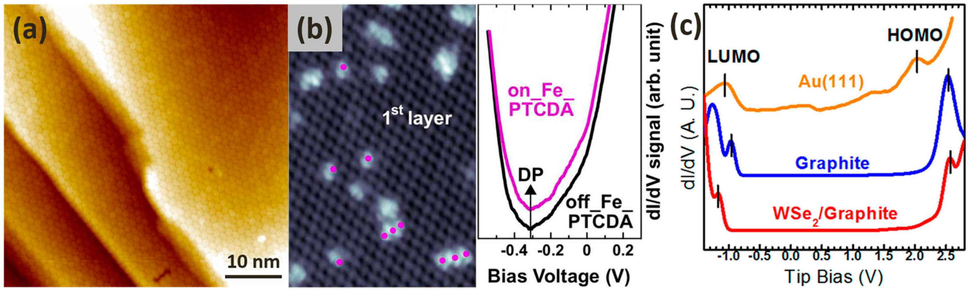
6. PTCDA on Layered Substrates

PTCDA usually forms an in-plane herringbone structure because of intermolecular hydrogen bonding. EG is continuously over SiC step edges due to its bottom-up growth mechanism [68]. Thus, the EG-covered SiC step edges would not hamper the carpet-like PTCDA growth. As demonstrated in Figure 7a, monolayer PTCDA in a herringbone arrangement follows EG continuously over bi- and tri- SiC bilayer steps. This confirms the possibility to grow a pinhole-free PTCDA monolayer on EG. Synchrotron-based PES investigation reveals weak charge transfer and weak interactions between PTCDA and EG [68]. It is important for the functionalization of the EG surface using PTCDA derivatives to enhance the adhesion of a gate dielectric layer on EG, facilitating the growth of defect-free ultrathin dielectric layers in G-based electronic devices.
Such a self-assembled PTCDA layer can also be used as a buffer layer to protect the topological surface states (TSSs) of Bi2Se3, which exhibits a Dirac cone-like dispersion similar to G [69]. Fe deposition on bare Bi2Se3 results in resonance states at Fe adatoms due to Coulomb scattering between the Fe adatoms and the TSSs, and the shift of the Dirac point (DP) energy position downward by ~80 meV (doping effect) due to charge transfer from the Fe adatoms to the Bi2Se3 surface. On the contrary, Fe deposition on one ML PTCDA covered Bi2Se3 results in neither resonance states nor doping effect, as shown in Figure 7b, because of the charge transfer from the Fe adatom to PTCDA molecules and concentration of the Coulomb charge. Thus, organic molecules are promising as spacers in the future TI devices to prevent undesirable doping and scattering effects at the interfaces.
The highest occupied molecular orbital-lowest unoccupied molecular orbital (HOMO-LUMO) gaps of small organic molecules are dependent on the electronic screening effects from the substrate. It is measured to be 3.73, 3.49, and 3.10 eV for PTCDA on SL WSe2/graphite (semiconducting), graphite (semimetallic), and Au(111) (metallic), respectively, as demonstrated in the scanning tunnelling spectroscopy (STS) results in Figure 7c, although the lattice parameters for these herringbone arrangements are very similar for the different substrates [70].Thus, the semiconducting 2D transition metal dichalcogenides (TMDs) layers can participate actively in hybrid organic−inorganic devices with tailored structures and properties.

7. Conclusions

2D layered-material templated growth is a newly developed method for fabricating high-quality organic semiconductor thin films with controllable morphologies, interface properties, molecular orientations, and electronic structures. G, MoS2, and h-BN show obviously different effects on the growth of pentacene, CuPc, and C8-BTBT, indicating slight differences in the interfacial interactions. PTCDA can be used as protecting layer due to its inherent intermolecular H-bonding. Large-scale high-quality 2D layered materials are required for future thinner organic (opto-) electronics like OLEDs, OPVs and OFETs.

Acknowledgments

We acknowledge the financial support from the National Natural Science Foundation (NSF) of China (Grants No. 11304398, 11334014, 51173205). Han Huang acknowledges the support from State Key Laboratory of Powder Metallurgy, Central South University and that from NSF of Hunan province (Grants No. 2016JJ1021).

Author Contributions

All authors contributed to the writing and production of this manuscript.

Conflicts of Interest

The authors declare no competing financial interests.

References

  1. Sokolov, A.N.; Tee, B.C.; Bettinger, C.J.; Tok, J.B.H.; Bao, Z. Chemical and engineering approaches to enable organic field-effect transistors for electronic skin applications. Acc. Chem. Res. 2011, 45, 361–371. [Google Scholar] [CrossRef] [PubMed]
  2. Figueira-Duarte, T.M.; Müllen, K. Pyrene-based materials for organic electronics. Chem. Rev. 2011, 111, 7260–7314. [Google Scholar] [CrossRef] [PubMed]
  3. Gao, Y. Surface analytical studies of interfaces in organic semiconductor devices. Mater. Sci. Eng. R 2010, 68, 39–87. [Google Scholar] [CrossRef]
  4. Qian, C.; Sun, J.; Zhang, L.; Xie, H.; Huang, H.; Yang, J.; Gao, Y. Air-stable and high-performance organic field-effect transistors based on ordered, large-domain phthalocyanine copper thin film. Synth. Met. 2015, 210, 336–341. [Google Scholar] [CrossRef]
  5. Huang, W.; Yang, B.; Sun, J.; Liu, B.; Yang, J.; Zou, Y.; Gao, Y. Organic field-effect transistor and its photoresponse using a benzo [1,2-b:4,5-b′] difuran-based donor–acceptor conjugated polymer. Org. Electron. 2014, 15, 1050–1055. [Google Scholar] [CrossRef]
  6. Koch, N.; Vollmer, A.; Salzmann, I.; Nickel, B.; Weiss, H.; Rabe, J.P. Evidence for temperature-dependent electron band dispersion in pentacene. Phys. Rev. Lett. 2006, 96, 156803. [Google Scholar] [CrossRef] [PubMed]
  7. Zhang, Y.; Qiao, J.; Gao, S.; Hu, F.; He, D.; Wu, B.; Ji, W. Probing Carrier Transport and Structure-Property Relationship of Highly Ordered Organic Semiconductors at the Two-Dimensional Limit. Phys. Rev. Lett. 2016, 116, 016602. [Google Scholar] [CrossRef] [PubMed]
  8. Sadowski, J.T.; Nagao, T.; Yaginuma, S.; Fujikawa, Y.; Al-Mahboob, A.; Nakajima, K.; Tromp, R.M. Thin bismuth film as a template for pentacene growth. Appl. Phys. Lett. 2005, 86, 073109. [Google Scholar] [CrossRef]
  9. Kakuta, H.; Hirahara, T.; Matsuda, I.; Nagao, T.; Hasegawa, S.; Ueno, N.; Sakamoto, K. Electronic structures of the highest occupied molecular orbital bands of a pentacene ultrathin film. Phys. Rev. Lett. 2007, 98, 247601. [Google Scholar] [CrossRef] [PubMed]
  10. Huang, H.; Huang, Y.; Pflaum, J.; Wee, A.T.S.; Chen, W. Nanoscale phase separation of a binary molecular system of copper phthalocyanine and di-indenoperylene on Ag (111). Appl. Phys. Lett. 2009, 95, 263309. [Google Scholar] [CrossRef]
  11. Zheng, F.; Park, B.N.; Seo, S.; Evans, P.G.; Himpsel, F.J. Orientation of pentacene molecules on SiO2: From a monolayer to the bulk. J. Chem. Phys. 2007, 126, 154702. [Google Scholar] [CrossRef] [PubMed]
  12. Ruiz, R.; Choudhary, D.; Nickel, B.; Toccoli, T.; Chang, K.C.; Mayer, A.C.; Malliaras, G.G. Pentacene thin film growth. Chem. Mater. 2004, 16, 4497–4508. [Google Scholar] [CrossRef]
  13. Wang, C.; Irfan, I.; Turinske, A.J.; Gao, Y. Pinning of fullerene lowest unoccupied molecular orbital edge at the interface with standing up copper phthalocyanine. Thin Solid Films 2012, 525, 64–67. [Google Scholar] [CrossRef]
  14. He, T.; Ding, H.; Peor, N.; Lu, M.; Corley, D.A.; Chen, B.; Tour, J.M. Silicon/molecule interfacial electronic modifications. J. Am. Chem. Soc. 2008, 130, 1699–1710. [Google Scholar] [CrossRef] [PubMed]
  15. Lee, W.H.; Park, J.; Sim, S.H.; Lim, S.; Kim, K.S.; Hong, B.H.; Cho, K. Surface-directed molecular assembly of pentacene on monolayer graphene for high-performance organic transistors. J. Am. Chem. Soc. 2011, 133, 4447–4454. [Google Scholar] [CrossRef] [PubMed]
  16. Wan, W.; Li, H.; Huang, H.; Wong, S.L.; Lv, L.; Gao, Y.; Wee, A.T.S. Incorporating isolated molybdenum (Mo) atoms into bilayer epitaxial graphene on 4H-SiC (0001). ACS Nano 2013, 8, 970–976. [Google Scholar] [CrossRef] [PubMed]
  17. Huang, H.; Wong, S.L.; Wang, Y.; Sun, J.T.; Gao, X.; Wee, A.T.S. Scanning tunneling microscope and photoemission spectroscopy investigations of bismuth on epitaxial graphene on SiC (0001). J. Phys. Chem. C 2014, 118, 24995–24999. [Google Scholar] [CrossRef]
  18. Wang, C.; Liu, X.; Wang, C.; Xu, X.; Li, Y.; Xie, F.; Gao, Y. Molecular orientation of copper phthalocyanine thin films on different monolayers of fullerene on SiO2 or highly oriented pyrolytic graphite. Appl. Phys. Lett. 2015, 106, 121603. [Google Scholar] [CrossRef]
  19. Wan, X.; Long, G.; Huang, L.; Chen, Y. Graphene–A promising material for organic photovoltaic cells. Adv. Mater. 2011, 23, 5342–5358. [Google Scholar] [CrossRef] [PubMed]
  20. Wassei, J.K.; Kaner, R.B. Graphene, a promising transparent conductor. Mater. Today 2010, 13, 52–59. [Google Scholar] [CrossRef]
  21. Radisavljevic, B.; Radenovic, A.; Brivio, J.; Giacometti, V.; Kis, A. Single-layer MoS2 transistors. Nat. Nanotechnol. 2011, 6, 147–150. [Google Scholar] [CrossRef] [PubMed]
  22. Liu, H.; Neal, A.T.; Ye, P.D. Channel length scaling of MoS2 MOSFETs. ACS Nano 2012, 6, 8563–8569. [Google Scholar] [CrossRef] [PubMed]
  23. Kim, S.; Konar, A.; Hwang, W.S.; Lee, J.H.; Lee, J.; Yang, J.; Jin, Y.W. High-mobility and low-power thin-film transistors based on multilayer MoS2 crystals. Nat. Commun. 2012, 3, 1011. [Google Scholar] [CrossRef] [PubMed]
  24. Xiao, J.; Long, M.; Li, X.; Xu, H.; Huang, H.; Gao, Y. Theoretical prediction of electronic structure and carrier mobility in single-walled MoS2 nanotubes. Sci. Rep. 2014, 4. [Google Scholar] [CrossRef] [PubMed]
  25. Jariwala, D.; Marks, T.J.; Hersam, M.C. Mixed-dimensional van der Waals heterostructures. Nat. Mater. 2016. [Google Scholar] [CrossRef] [PubMed]
  26. Geim, A.K.; Grigorieva, I.V. Van der Waals heterostructures. Nature 2013, 499, 419–425. [Google Scholar] [CrossRef] [PubMed]
  27. Chen, H.; Wen, X.; Zhang, J.; Wu, T.; Gong, Y.; Zhang, X.; Zhuang, W. Ultrafast formation of interlayer hot excitons in atomically thin MoS2/WS2 heterostructures. Nat. Commun. 2016, 7, 12512. [Google Scholar] [CrossRef] [PubMed]
  28. Pierucci, D.; Henck, H.; Avila, J.; Balan, A.; Naylor, C.H.; Patriarche, G.; Asensio, M.C. Band alignment and minigaps in monolayer MoS2-graphene van der Waals heterostructures. Nano Lett. 2016, 16, 4054–4061. [Google Scholar] [CrossRef] [PubMed]
  29. Coy Diaz, H.; Avila, J.; Chen, C.; Addou, R.; Asensio, M.C.; Batzill, M. Direct observation of interlayer hybridization and Dirac relativistic carriers in graphene/MoS2 van der Waals heterostructures. Nano Lett. 2015, 15, 1135–1140. [Google Scholar] [CrossRef] [PubMed]
  30. Shih, C.-J.; Wang, Q.H.; Son, Y.; Jin, Z.; Blankschtein, D.; Strano, M.S. Tuning On−Off Current Ratio and Field-Effect Mobility in a MoS2−Graphene Heterostructure via Schottky Barrier Modulation. ACS Nano 2014, 8, 5790–5798. [Google Scholar] [CrossRef] [PubMed]
  31. Sadowski, J.T.; Sazaki, G.; Nishikata, S.; Al-Mahboob, A.; Fujikawa, Y.; Nakajima, K.; Sakurai, T. Single-nucleus polycrystallization in thin film epitaxial growth. Phys. Rev. Lett. 2007, 98, 046104. [Google Scholar] [CrossRef] [PubMed]
  32. Al-Mahboob, A.; Sadowski, J.T.; Nishihara, T.; Fujikawa, Y.; Xue, Q.K.; Nakajima, K.; Sakurai, T. Epitaxial structures of self-organized, standing-up pentacene thin films studied by LEEM and STM. Surf. Sci. 2007, 601, 1304–1310. [Google Scholar] [CrossRef]
  33. Kelley, T.W.; Baude, P.F.; Gerlach, C.; Ender, D.E.; Muyres, D.; Haase, M.A.; Theiss, S.D. Recent progress in organic electronics: Materials, devices, and processes. Chem. Mater. 2004, 16, 4413–4422. [Google Scholar] [CrossRef]
  34. Lu, J.; Yeo, P.S.E.; Zheng, Y.; Xu, H.; Gan, C.K.; Sullivan, M.B.; Loh, K.P. Step flow versus mosaic film growth in hexagonal boron nitride. J. Am. Chem. Soc. 2013, 135, 2368–2373. [Google Scholar] [CrossRef] [PubMed]
  35. Götzen, J.; Käfer, D.; Wöll, C.; Witte, G. Growth and structure of pentacene films on graphite: Weak adhesion as a key for epitaxial film growth. Phys. Rev. B 2010, 81, 085440. [Google Scholar] [CrossRef]
  36. Zhang, L.; Roy, S.S.; Hamers, R.J.; Arnold, M.S.; Andrew, T.L. Molecular Orientation-Dependent Interfacial Energetics and Built-in Voltage Tuned by a Template Graphene Monolayer. J. Phys. Chem. C 2014, 119, 45–54. [Google Scholar] [CrossRef]
  37. Salzmann, I.; Moser, A.; Oehzelt, M.; Breuer, T.; Feng, X.; Juang, Z.Y.; Brillante, A. Epitaxial growth of π-stacked perfluoropentacene on graphene-coated quartz. ACS Nano 2012, 6, 10874–10883. [Google Scholar] [CrossRef] [PubMed]
  38. Kholmanov, I.N.; Gavioli, L.; Fanetti, M.; Casella, M.; Cepek, C.; Mattevi, C.; Sancrotti, M. Effect of substrate surface defects on the morphology of Fe film deposited on graphite. Surf. Sci. 2007, 601, 188–192. [Google Scholar] [CrossRef]
  39. Mao, H.Y.; Wang, R.; Wang, Y.; Niu, T.C.; Zhong, J.Q.; Huang, M.Y.; Chen, W. Chemical vapor deposition graphene as structural template to control interfacial molecular orientation of chloroaluminium phthalocyanine. Appl. Phys. Lett. 2011, 99, 093301. [Google Scholar]
  40. Jariwala, D.; Howell, S.L.; Chen, K.S.; Kang, J.; Sangwan, V.K.; Filippone, S.A.; Hersam, M.C. Hybrid, Gate-Tunable, van der Waals p–n Heterojunctions from Pentacene and MoS2. Nano Lett. 2015, 16, 497–503. [Google Scholar] [CrossRef] [PubMed]
  41. Furchi, M.M.; Pospischil, A.; Libisch, F.; Burgdörfer, J.; Mueller, T. Photovoltaic effect in an electrically tunable van der Waals heterojunction. Nano Lett. 2014, 14, 4785–4791. [Google Scholar] [CrossRef] [PubMed]
  42. Lee, C.H.; Lee, G.H.; Van Der Zande, A.M.; Chen, W.; Li, Y.; Han, M.; Guo, J. Atomically thin p-n junctions with van der Waals heterointerfaces. Nat. Nanotechnol. 2014, 9, 676–681. [Google Scholar] [CrossRef] [PubMed]
  43. Jariwala, D.; Sangwan, V.K.; Seo, J.W.T.; Xu, W.; Smith, J.; Kim, C.H.; Hersam, M.C. Large-area, low-voltage, antiambipolar heterojunctions from solution-processed semiconductors. Nano Lett. 2014, 15, 416–421. [Google Scholar] [CrossRef] [PubMed]
  44. Xiong, F. Amplitude shift keying. In Encyclopedia of RF and Microwave Engineering; John Wiley & Sons, Inc.: Hoboken, NJ, USA, 2005. [Google Scholar]
  45. Mativetsky, J.M.; Wang, H.; Lee, S.S.; Whittaker-Brooks, L.; Loo, Y.L. Face-on stacking and enhanced out-of-plane hole mobility in graphene-templated copper phthalocyanine. Chem. Commun. 2014, 50, 5319–5321. [Google Scholar] [CrossRef] [PubMed]
  46. Della Pirriera, M.; Puigdollers, J.; Voz, C.; Stella, M.; Bertomeu, J.; Alcubilla, R. Optoelectronic properties of CuPc thin films deposited at different substrate temperatures. J. Phys. D Appl. Phys. 2009, 42, 145102. [Google Scholar] [CrossRef]
  47. Bao, Z.; Lovinger, A.J.; Dodabalapur, A. Organic field-effect transistors with high mobility based on copper phthalocyanine. Appl. Phys. Lett. 1996, 69, 3066–3068. [Google Scholar] [CrossRef]
  48. Xiao, K.; Deng, W.; Keum, J.K.; Yoon, M.; Vlassiouk, I.V.; Clark, K.W.; Li, A.-P.; Kravchenko, I.I.; Gu, G.; Payzant, E.A.; et al. Surface-induced orientation control of CuPc molecules for the epitaxial growth of highly ordered organic crystals on graphene. J. Am. Chem. Soc. 2013, 135, 3680–3687. [Google Scholar] [CrossRef] [PubMed]
  49. Jeong, J.; Park, S.; Kang, S.J.; Lee, H.; Yi, Y. Impacts of Molecular Orientation on the Hole Injection Barrier Reduction: CuPc/HAT-CN/Graphene. J. Phys. Chem. C 2016, 120, 2292–2298. [Google Scholar] [CrossRef]
  50. Zhang, L.; Yang, Y.; Huang, H.; Lyu, L.; Zhang, H.; Cao, N.; Gao, Y. Thickness-dependent air-exposure-induced phase transition of CuPc ultrathin films to well-ordered one-dimensional nanocrystals on layered substrates. J. Phys. Chem. C 2015, 119, 4217–4223. [Google Scholar] [CrossRef]
  51. Cao, N.-T.; Zhang, L.; Lü, L.; Xie, H.-P.; Huang, H.; Niu, D.-M.; Gao, Y.-L. van der Waals heterostructure about CuPc/MoS2 (0001). Acta Phys. Sin. 2014, 63, 167903. [Google Scholar]
  52. Pak, J.; Jang, J.; Cho, K.; Kim, T.Y.; Kim, J.K.; Song, Y.; Lee, T. Enhancement of photodetection characteristics of MoS2 field effect transistors using surface treatment with copper phthalocyanine. Nanoscale 2015, 7, 18780–18788. [Google Scholar] [CrossRef] [PubMed]
  53. Hosoi, Y.; Deyra, D.M.; Nakajima, K.; Furukawa, Y. Micro-Raman spectroscopy on pentacene thin-film transistors. Mol. Crys. Liq. Crys. 2008, 491, 317–323. [Google Scholar] [CrossRef]
  54. Chhikara, M.; Pavlica, E.; Matković, A.; Gajić, R.; Bratina, G. Effect of Water Layer at the SiO2/Graphene Interface on Pentacene Morphology. Langmuir 2014, 30, 11681–11688. [Google Scholar] [CrossRef] [PubMed]
  55. Ling, X.; Fang, W.; Lee, Y.H.; Araujo, P.T.; Zhang, X.; Rodriguez-Nieva, J.F.; Dresselhaus, M.S. Raman enhancement effect on two-dimensional layered materials: Graphene, h-BN and MoS2. Nano Lett. 2014, 14, 3033–3040. [Google Scholar] [CrossRef] [PubMed]
  56. He, D.; Zhang, Y.; Wu, Q.; Xu, R.; Nan, H.; Liu, J.; Shi, Y. Two-dimensional quasi-freestanding molecular crystals for high-performance organic field-effect transistors. Nat. Commun. 2014, 5, 5162. [Google Scholar] [CrossRef] [PubMed]
  57. He, D.; Pan, Y.; Nan, H.; Gu, S.; Yang, Z.; Wu, B.; Ni, Z. A van der Waals pn heterojunction with organic/inorganic semiconductors. Appl. Phys. Lett. 2015, 107, 183103. [Google Scholar] [CrossRef]
  58. Wang, Q.H.; Kalantar-Zadeh, K.; Kis, A.; Coleman, J.N.; Strano, M.S. Electronics and optoelectronics of two-dimensional transition metal dichalcogenides. Nat. Nanotechnol. 2012, 7, 699–712. [Google Scholar] [CrossRef] [PubMed]
  59. Sachs, B.; Britnell, L.; Wehling, T.O.; Eckmann, A.; Jalil, R.; Belle, B.D.; Novoselov, K.S. Doping mechanisms in graphene-MoS2 hybrids. Appl. Phys. Lett. 2013, 103, 251607. [Google Scholar] [CrossRef]
  60. Hong, J.; Hu, Z.; Probert, M.; Li, K.; Lv, D.; Yang, X.; Zhang, J. Exploring atomic defects in molybdenum disulphide monolayers. Nat. Commun. 2015, 6, 6293. [Google Scholar] [CrossRef] [PubMed]
  61. Yu, Z.; Pan, Y.; Shen, Y.; Wang, Z.; Ong, Z.Y.; Xu, T.; Wang, J. Towards intrinsic charge transport in monolayer molybdenum disulfide by defect and interface engineering. Nat. Commun. 2014, 5, 5290. [Google Scholar] [CrossRef] [PubMed]
  62. Smits, E.C.; Mathijssen, S.G.; Van Hal, P.A.; Setayesh, S.; Geuns, T.C.; Mutsaers, K.A.; Kemerink, M. Bottom-up organic integrated circuits. Nature 2008, 455, 956–959. [Google Scholar] [CrossRef]
  63. Li, L.; Gao, P.; Wang, W.; Müllen, K.; Fuchs, H.; Chi, L. Growth of ultrathin organic semiconductor microstripes with thickness control in the monolayer precision. Angew. Chem. Int. Ed. 2013, 52, 12530–12535. [Google Scholar] [CrossRef] [PubMed]
  64. Mathijssen, S.G.; Smits, E.C.; van Hal, P.A.; Wondergem, H.J.; Ponomarenko, S.A.; Moser, A.; de Leeuw, D.M. Monolayer coverage and channel length set the mobility in self-assembled monolayer field-effect transistors. Nat. Nanotechnol. 2009, 4, 674–680. [Google Scholar] [CrossRef] [PubMed]
  65. Dinelli, F.; Murgia, M.; Levy, P.; Cavallini, M.; Biscarini, F.; de Leeuw, D.M. Spatially correlated charge transport in organic thin film transistors. Phys. Rev. Lett. 2004, 92, 116802. [Google Scholar] [CrossRef] [PubMed]
  66. Ruiz, R.; Papadimitratos, A.; Mayer, A.C.; Malliaras, G.G. Thickness Dependence of Mobility in Pentacene Thin-Film Transistors. Adv. Mater. 2005, 17, 1795–1798. [Google Scholar] [CrossRef]
  67. Wu, B.; Zhao, Y.; Nan, H.; Yang, Z.; Zhang, Y.; Zhao, H.; Shi, Y. Precise, self-limited epitaxy of ultrathin organic semiconductors and heterojunctions tailored by van der Waals interactions. Nano Lett. 2016, 6, 3754–3759. [Google Scholar] [CrossRef] [PubMed]
  68. Huang, H.; Chen, S.; Gao, X.; Chen, W.; Wee, A.T.S. Structural and electronic properties of PTCDA thin films on epitaxial graphene. ACS Nano 2009, 3, 3431–3436. [Google Scholar] [CrossRef] [PubMed]
  69. Yang, H.H.; Chu, Y.H.; Lu, C.I.; Butler, C.J.; Sankar, R.; Chou, F.C.; Lin, M.T. Organic Monolayer Protected Topological Surface State. Nano Lett. 2015, 15, 6896–6900. [Google Scholar] [CrossRef] [PubMed]
  70. Zheng, Y.J.; Huang, Y.L.; Chen, Y.; Zhao, W.; Eda, G.; Spataru, C.D.; Quek, S.Y. Heterointerface Screening Effects between Organic Monolayers and Monolayer Transition Metal Dichalcogenides. ACS Nano 2016, 10, 2476–2484. [Google Scholar] [CrossRef] [PubMed]
Figure 1. Molecular structures of pentacene (a), CuPc (b), PTCDA (c), C8-BTBT (d), respectively. (e) The a-b and b-c planes of a pentacene single crystal, showing the anisotropy of small organic molecules. (f) Schematics of three layered substrates, G, MoS2 and h-BN.
Crystals 06 00113 g001
Figure 2. Morphologies of pentacene thin films on different substrates. (a) AFM topography image of fractal islands of pentacene on SiO2 at a coverage of ~3 ML. Inset: nucleation at submonolayer coverage. (b) STM image of pentacene on Bi(001) at a coverage of slightly over 1 ML. Inset: high-resolution STM image showing pentacene molecules in the first layer in a standing-up configuration. (c) Twelve nanometer thick pentacene film on Highly Oriented Pyrolytic Graphite (HOPG). (df) Schematic representations of the proposed molecular packing corresponding to image in panel (ac). Panel a reprinted with permission from [12]. Copyright 2004 American Chemical Society. Panel b reprinted from [8] with the permission of AIP Publishing. Panels c, f reprinted with permission from [6] as follows: Koch, N. Physical review letters, 96 (15), 156803, 2006. Copyright 2006, American Physical Society.
Crystals 06 00113 g002
Figure 3. Epitaxial growth of pentacene molecular crystals on layered substrates. (a) AFM image of ~50 nm thick pentacene films over the sharp linear boundary between G-covered and bare SiO2. (b) Forty nanometer pentacene films over the boundary between MoS2-covered and bare SiO2. (c) Approximately two ML pentacene crystals with a flat-lying wetting layer on mechanically exfoliated h-BN. (df) Schematic illustrations of the molecular packing of (ac), respectively. (gi) The transfer characteristics of FETs based on the films in (ac), respectively. Panel a,d,g reprinted with permission from [15]. Copyright 2011 American Chemical Society. Panel b, h reprinted with permission from [40]. Copyright 2015 American Chemical Society. Panel c, f, i reprinted with permission from [7] as follows: Zhang, Y. Physical review letters, 116 (1), 016602, 2016. Copyright 2016 American Physical Society.
Crystals 06 00113 g003
Figure 4. The AFM morphologic images and 2D-GIXRD images of CuPc on glass (a,d), G-covered glass (b,e), and bulk MoS2 (c,f), respectively. The insets show the corresponding CuPc packing. Panel a, b, d, e is reproduced from [45] with permission from The Royal Society of Chemistry. Panel c, f is reprinted with permission from [50], copyright 2015 American Chemical Society.
Crystals 06 00113 g004
Figure 5. (a) Raman spectra from pentacene on glass without/with monolayer G, and from G on glass. (λ = 532 nm; 3.0 mW). (b) Raman spectra from 2 Å thick CuPc on G (blue line), on h-BN (red line), on MoS2 (green line), and on the blank SiO2/Si substrate (black line). Panel a reprinted with permission from [36], copyright 2015 American Chemical Society. Panel b reprinted with permission from [55], copyright 2015 American Chemical Society.
Crystals 06 00113 g005
Figure 6. C8-BTBT on layered substrates. AFM image of C8-BTBT on G (a) and MoS2 (b). (c) Transfer characteristic of 1L C8-BTBT/h-BN based planar OFET at room temperature. Black and blue lines are drawn in linear and log scales, respectively. Inset shows the optical microscopy image of the device. (d) Blue dots: calculated binding energies of a single C8-BTBT molecule on G, IL/G, 1L/IL/G, and 2L/1L/IL/G. Red dash line: C8-BTBT−C8-BTBT interaction. Inset shows the molecular structure of C8-BTBT and molecular packing of different C8-BTBT layers on G. (e) AFM images of SLOMBE of bilayer C8-BTBT on PTCDA. (f) Output characteristics of the p-n junction (>15 nm) under the dark conditions (black) and under the 0.67 μW laser illumination. Inset shows schematic layout of the device. Panel a, c reprinted with permission from [56], copyright 2014, Nature Publishing Group. Panel b reprinted from [57], with the permission of AIP Publishing. Panel d, e, f adapted with permission from [67], copyright 2016 American Chemical Society.
Crystals 06 00113 g006
Figure 7. PTCDA on layered substrates. (a) Molecularly-resolved STM image of one monolayer PTCDA covered epitaxial G on SiC(0001). (b) STM image of ~0.01 ML Fe (protrusions) on one monolayer PTCDA covered Bi2Se3 (left) and STS curves at positions with/without Fe (purple/black, right). (c) STS curves at positions of PTCDA on Au(111), graphite, and WSe2/graphite. Panel a printed with permission from [68], copyright 2009 American Chemical Society. Panel b printed with permission from [69], copyright 2015 American Chemical Society. Panel c printed with permission from [70], copyright 2016 American Chemical Society.
Crystals 06 00113 g007

