
Recent Advances in the Raman Investigation of Structural and Optical Properties of Graphene and Other Two-Dimensional Materials

1
Department of Information Engineering, Infrastructures and Sustainable Energy (DIIES), University “Mediterranea” of Reggio Calabria, 89122 Reggio Calabria, Italy
2
Dipartimento di Fisica, Università della Calabria, 87036 Rende, Italy
3
Licryl CNR/Nanotec c/o Dipartimento di Fisica, Università della Calabria, 87036 Rende, Italy
*
Author to whom correspondence should be addressed.
Crystals 2023, 13(9), 1357; https://doi.org/10.3390/cryst13091357
Submission received: 16 August 2023
/
Revised: 2 September 2023
/
Accepted: 6 September 2023
/
Published: 8 September 2023
(This article belongs to the Special Issue Recent Advances in Graphene and Other Two-Dimensional Materials)
Abstract
:This research work presents our recent advancements in the study of graphene and other two-dimensional (2D) materials. This review covers studies on graphene oxide (GO) thin films deposited on various substrates, including titanium and silver thin films. The analysis reveals the role of surface-enhanced Raman scattering (SERS) and the influence of film thickness and laser intensity on the observed Raman peaks. Investigations of a silver/GO/gold sandwich structure demonstrate the presence of sharp Raman modes attributed to localized surface plasmon resonances. This review also discusses the characterization of exfoliation-synthesized graphene nanoplatelet (GNPs) thin films and of single-layer graphene deposited via chemical vapor deposition (CVD). The optical properties of molybdenum disulfide (MoS2) films are also explored. The utilization of micro-Raman spectroscopy provides valuable insights into the structural and optical properties of graphene and other 2D materials. These results hold the potential to drive advancements in various applications, such as electronics, photonics, and nanocomposites.
1. Introduction
Graphene and other two-dimensional (2D) materials display exceptional characteristics, making them highly advantageous for a diverse range of applications across various fields [1,2,3,4,5,6,7,8], including flexible nanoelectronics, sensors, and photodetectors [9,10,11,12,13,14,15,16,17].
Graphene exhibits special physical and electrical properties. It demonstrates broad light absorption, a linear dispersion band structure, significant charge-carrier mobility, and remarkable optical qualities. For instance, it offers high transparency within the visible spectrum [18], photo-response capabilities extending into the Terahertz frequency range, and customizable infrared optical absorbance [19]. Furthermore, its unique band structure and electron transport properties make it a promising candidate for developing high-performance modulators, sources, and detectors designed for operation in the infrared (IR) segment of the electromagnetic spectrum [20]. The optical characteristics of graphene films vary significantly depending on the fabrication method used, whether it is exfoliation or chemical vapor deposition (CVD) [14]. CVD, a method intended for producing high-quality few-layer graphene, has been successfully applied in ultradense photonic, optoelectronic, and electronic devices, as described in previous research [21,22].
Recently, there has been growing interest in combining the unique properties of graphene-based materials with silver nanostructures, aiming for their utilization in the fields of plasmonics and metamaterials applications [23,24,25]. Silver nanoparticles and nanostructures, with localized surface plasmonic resonance spanning from the visible to the near-infrared range, find utility in various applications, particularly in surface-enhanced Raman scattering (SERS) [26]. In this context, materials based on graphene, for instance, graphene oxide (GO) and reduced graphene oxide (RGO), have demonstrated their potential as SERS substrates by generating strong chemical enhancement [27].
Nevertheless, even with substantial endeavors by the scientific community, attaining widespread accessibility to graphene samples remains a considerable obstacle, hindering the exploitation of its exceptional application capabilities [28]. Consequently, while single-layer graphene is not readily accessible for large-scale bulk applications, materials related to graphene, including RGO, few-layer graphene, multilayer graphene, and graphene nanoplatelets (GNPs), have emerged as pioneering materials with numerous potential applications [29].
GO has emerged as a novel nanomaterial based on carbon that provides a different pathway to graphene [30]. By utilizing robust oxidizing agents in processes like the Hummers method, graphite undergoes oxidation, leading to the incorporation of diverse oxidized functional groups, such as epoxide, carbonyl, carboxyl, and hydroxyl groups, into its molecular framework [31,32,33]. This process widens the gaps between layers and imparts hydrophilic properties to the material. As a result, graphite oxide can be effectively dispersed in water via ultrasonic treatment, ultimately yielding the fabrication of individual or a limited number of GO layers [34].
GNPs, which are another graphene-based material, possess several advantageous characteristics akin to those of monolayer graphene [35,36]. When comprised of a monolayer to a small number of layers, these sheets consist of sp2-bonded carbon atoms that interlock, forming particles with a 2D nanoarchitecture on the scale of nanometers. These particles are realized through the exfoliation of low-cost graphite flakes, followed by chemical treatment and the reduction of graphite oxide nanoplatelets [37,38,39].
Recent advancements have also been reported in the field of metal dichalcogenides (WS2, MoS2, MoSe2, WSe2) films [40]. Transition metal dichalcogenide (TMD) materials, because of their exceptional optoelectronic characteristics, hold various potential applications when combined with conducting materials [41]. Some of these applications include hydrogen evolution, Li-ion batteries, solar cells, and supercapacitors [42,43].
2. Structure of Graphene, Graphene Oxide, and Reduced Graphene Oxide
Graphene consists of a single layer of carbon atoms arranged in a hexagonal lattice and originates from graphite [50]. Its unique properties include sp2 hybridization and an incredibly slim atomic thickness measuring 0.345 nm [51]. A perfect graphene sheet has a flat structure with minor ripples, and its carbon atoms form a trigonal pattern [52]. Various methods have been developed to fabricate graphene, including CVD [53], epitaxial growth [54], micromechanical exfoliation [55], and epitaxial growth on insulating surfaces like SiC [56]. These techniques have significantly advanced research on monolayer graphene.
GO, on the other hand, is a derivative of graphene that contains oxygen-functional groups like epoxide, carbonyl, carboxyl, and hydroxy [57]. These groups render GO sheets water-soluble; their removal leads to flocculation and precipitation. GO features a complex structure with oxygen-rich domains interspersed among areas where carbon atoms retain their sp2 hybridization [58].
Graphite and graphite oxide, although related, have distinct properties [59]. Graphite oxide is created by oxidizing graphite, which introduces oxygen functionalities that increase the distance between layers and make the material water-dispersible [60]. Exfoliation of graphite oxide through sonication in water results in the formation of GO [61]. The primary difference between graphite oxide and GO is in the number of layers: graphite oxide is multilayered, while GO dispersions mainly consist of monolayer flakes, with some multilayer flakes present [62].
Zeta potential measurements show that GO sheets in water carry negative charges [63], which leads to electrostatic repulsion among the sheets and results in a stable aqueous suspension. The utilization of organic compounds in chemically altering GO sheets can lead to the attainment of uniform dispersions in organic solvents [64].
A widely employed technique for synthesizing GO is the adapted Hummers method, which relies on oxidizing graphite by using a blend of concentrated sulfuric acid, sodium nitrate, and potassium permanganate [65]. While the exact chemical arrangement of GO remains not entirely comprehended, it is considered partially amorphous, with proposed structural models consisting of hydroxyl and epoxy functional groups [66]. Analysis conducted using atomic force microscopy has unveiled that the thickness of a single-layer GO sheet can exhibit fluctuations ranging from 0.7 to 1.4 nm, notably surpassing the thickness of an ideal graphene monolayer [67].
Various techniques, such as drop-casting [68], dip-coating [69], spraying [70], spin-coating [71], and electrophoresis [72], can be used to deposit GO sheets as thin films on different substrates.
GO and graphene have also been extensively used to obtain composite coatings, enhancing the wear behavior and other mechanical properties of the substrate. For example, in Ref. [73], an enhanced wear behavior in nickel/graphene composite coatings is reported. Similarly, in Ref. [74], the properties of nickel-based composite coatings modified with GO are investigated.
The electrical properties of GO sheets differ significantly from those of pristine graphene. As a consequence, films composed of GO tend to manifest resistance values that commonly exceed 1012 Ω/sq [75].
A partial reduction of GO can yield sheets resembling graphene by eliminating oxygen-related groups [76]. Chemical reduction methods typically use reducing agents such as hydrazine or involve creating highly alkaline conditions [77]. Ascorbic acid has emerged as a promising alternative to hydrazine [78]. The thermal reduction process for GO is commonly conducted at temperatures exceeding 200 °C within inert or reducing surroundings, with an enhanced efficacy observed at elevated temperatures [79].
Understanding the methods of reducing GO is pivotal, as the process not only alters its hydrophilicity but also has a profound impact on its electrical conductivity, thereby influencing its suitability for various applications.
These reduced GO sheets exhibit reduced hydrophilicity and display a propensity to aggregate within the solution, stemming from the absence of oxygenated functionalities [80]. The chemical reduction of GO partially restores its conductivity [81], yet it remains significantly inferior by several orders of magnitude when compared to the pristine graphene counterpart. The degree of this reduction determines the conductivity of the resulting RGO, which can range from 0.05 to 500 S/cm and is intricately linked to the proportion of graphitic (sp2) to oxidized (sp3) zones [82].
It remains a significant challenge to develop a production method for RGO that closely mimics the properties of pristine graphene. However, due to its moderate conductivity and the ability to be produced into a thin film through an aqueous solution, RGO is attractive for use in electronic devices. Additionally, GO and RGO find applications in nanocomposite materials, polymer composites, energy storage, and biomedical uses like drug delivery and catalysis [83].
3. State of the Art
Raman spectroscopy has become an indispensable tool for comprehensively characterizing graphene and its derivatives like GO and RGO [84,85]. The technique’s ability to identify characteristic vibrational modes in materials offers an understanding of the structural and chemical compositions of these graphene-based materials [86]. For example, Neeraj Sharma and colleagues [87] showed that the presence or absence of functional groups significantly alters the material’s vibrational modes, evident from changes in the Raman spectra [86]. This is particularly valuable for researchers aiming to tailor the properties of graphene-based materials for specific applications, such as optoelectronics or sensing.
The G and D peaks in the Raman spectra serve as critical markers for the structural integrity and chemical modifications of graphene-based materials [84]. The G peak, a fundamental graphitic peak, is ubiquitous in all hexagonal graphitic structures, while the D peak arises due to imperfections and impurities introduced by functional groups [84].
Jiang-Bin Wu and colleagues [88] further elaborate on how Raman spectroscopy can study the impact of various external factors like doping agents, mechanical forces, and environmental conditions on single-layer graphene. Additionally, the authors provide insights into the identification of material defects and layer counts through Raman spectral features.
K. Kanishka H. De Silva et al. [89] further extend this discussion by emphasizing the challenges posed by the abundant lattice defects in GO and RGO. Their work provides new insights into the optical visibility and Raman signals of these materials when deposited on different Si-based substrates. They found that dielectric substrates with lower reflectance in the visible range offer better optical contrast and more intense Raman signals. This advancement is significant because it implies that substrate choice can affect the quality of Raman spectroscopic data and, consequently, our understanding of the material’s structural and optical properties. Moreover, De Silva et al. [89] introduced the importance of the D’ band in the Raman spectra for a more comprehensive understanding of the structural variations in monolayer flakes of GO and RGO.
The existing literature on Raman spectroscopy for characterizing graphene and 2D materials is extensive [90]; however, our review introduces several unique contributions that set it apart from previous works.
A standout feature of our review explores magnetron sputtering as a deposition technique and its implications for SERS. While SERS is a well-known technique for enhancing Raman signals, its application in 2D materials deposited via magnetron sputtering is less commonly discussed. Our review delves into how magnetron sputtering can influence the SERS properties of 2D materials, offering new avenues for highly sensitive detection methods in both industrial and research settings.
Another unique aspect of our review is the focus on solution-based MoS2. While MoS2 has been extensively studied, few works have addressed the unique challenges and opportunities presented by solution-based methods. Our review fills this gap by discussing the Raman characterization of solution-based MoS2, offering a more comprehensive understanding of this material in liquid-phase environments. This is particularly relevant for applications where solution-based methods offer advantages in terms of scalability and cost-effectiveness.
4. Materials and Methods
Micro-Raman spectra [44,45,46,47,48,49] were obtained using a Horiba-Jobin Yvon micro-probe instrument with an approximate spectral resolution of 2 cm−1. This setup incorporated a CCD detector boasting dimensions of 256 × 1024 pixels, cooled to −70 °C, and was coupled with a diode laser emitting a 532 nm line, generating an output power of 50 mW. A 50× Mplan Olympus objective was used to focus the laser, yielding a laser spot with an apparent diameter of approximately 2–3 µm. To avert the structural modifications stemming from laser-induced heating, an OD2 filter with a 1% transmission rate was deployed.
The GO dispersions of the GO discussed were sourced from Sigma Aldrich (St. Louis, MO, USA) and Punto Quantico (Roma, Italy). The dispersion of MoS2 was bought from Sigma Aldrich (St. Louis, MO, USA). Monolayer graphene samples, grown via CVD, were procured from Graphenea Co. (San Sebastián, Spain).
5. Results and Discussion
This section provides a comprehensive analysis of graphene and other 2D materials, employing micro-Raman spectroscopy as the principal investigative tool. The focus spans from the electrophoretic deposition techniques of GO to the complex Ag/GO/Au sandwich structure. Each subsection aims to elucidate the unique structural and spectral characteristics of these materials, thereby contributing to the understanding of their potential applications and underlying mechanisms.
5.1. Thin Films of Graphene Oxide and Reduced Graphene Oxide Deposited by Electrophoresis
The electrophoretic deposition (EPD) method is highly adaptable for creating GO-based thin films. Charged GO platelets in a suspension move toward an electrode with an opposing charge under an applied electric field, forming a compact film. EPD offers advantages like a rapid deposition rate, controllable thickness, uniformity, and scalability. It requires electrically conductive substrates like Cu, Ni, Al, stainless steel, and Ti [91].
Figure 1a presents the Raman spectrum of electrophoretically deposited GO on a titanium layer before the annealing treatment.
The Raman spectrum shows characteristic peaks, specifically at 1329 cm−1 for the D band and 1592 cm−1 for the G band of GO. Additionally, the 2D band (≈2640 cm−1) and the second-order band, D+G (≈2912 cm−1), can be observed. These spectral features suggest a considerable level of disorder in the GO.
Figure 1b illustrates the GO film deposited on a titanium layer after the annealing at 400 °C. In this case, the D band is detected at about 1343 cm−1, indicating either a different level of carbon layer oxidation or varying mechanical stresses on the graphene layer.
5.2. Graphene Oxide on Magnetron-Sputtered Silver Thin Films for Surface-Enhanced Raman Spectroscopy Applications
GO’s potential in SERS is increasingly recognized. In this section, we look at how GO behaves when deposited on silver substrates deposited through magnetron sputtering.
Visual examination reveals two distinct types of GO deposition on the magnetron-sputtered silver substrate, as evident in Figure 2’s optical microscopy image.
The first type maintains optical properties like color and reflectivity, similar to the unaltered silver surface. These “bright” areas indicate the presence of a single or a few layers. Conversely, the remaining areas, referred to as “dark”, appear brown and show reduced reflectivity compared to the original silver surface.
The spectrum in Figure 3b comes from a “medium dark zone”, where GO is dip-coated on a 10 nm magnetron-sputtered silver substrate using low laser intensity (OD2). It reveals that the D and G Raman bands align with the frequencies observed in Figure 3a, where GO was dip-coated on untreated glass using the same experimental parameters. Significantly, the intensities of the D and G bands are markedly increased.
In Figure 3b, we observe distinct peaks at 235 cm−1, 967 cm−1, 1793 cm−1, and 2033 cm−1. These distinctive peaks were mostly pronounced in the “medium dark zones” compared to the “bright zones” and “dark zones.” Specifically, the peaks at 1793 cm−1 and 2033 cm−1 can be attributed to oxygen functionalities on the GO surface, likely C=O stretching vibrations from the carbonyl and carboxylic groups. The peaks at 235 cm−1 and 967 cm−1 can be associated with the existence of oxide in the silver thin films. This interaction between oxygen and silver thin films could result from the subsequent reactions occurring after deposition in ambient conditions.
Figure 4 presents the Raman spectrum from the same spot in the “medium dark zone”, as indicated in Figure 3b. However, this measurement uses the full laser intensity without any filtering.
Figure 4 shows a shift to lower frequencies in the D band, around 1343 cm−1, compared to Figure 3b. This could indicate a different level of oxidation in the GO layer. Meanwhile, the G band remained at the identical frequency of 1595 cm−1, as shown in Figure 3b. Moreover, a prevalent reduction in the intensity of the features at 235 cm−1, 967 cm−1, 1793 cm−1, and 2033 cm−1 is evident when compared with the spectrum presented in Figure 3b. These observations suggest a significant variation in the coupling between GO and silver when subjected to full laser power irradiation, leading to irreversible damage to the GO layer.
5.3. Micro-Raman Spectroscopy Measurements of Spin-Coated MoS2 Films
In this subsection, we explore the properties of spin-coated MoS2 films on Si/SiO2 substrates using micro-Raman spectroscopy.
The primary Raman modes of MoS2 include E1g (286 cm−1), E2g1 (383 cm−1), A1g (408 cm−1), and E2g2 (32 cm−1). The E1g, E2g1, and E2g2 modes are indicative of in-plane Raman activity, whereas the A1g mode signifies out-of-plane vibrations. Figure 5 shows typical Raman spectra from MoS2 films spin-coated onto Si/SiO2 substrates. These spectra originate from distinct locations on the samples.
In Figure 5a, only the E2g1 and A1g modes are present, appearing at approximately 380 cm−1 and 405 cm−1, correspondingly.
The location of the higher-frequency mode signifies the presence of a monolayer MoS2 specimen, whereas the alternate mode implies a structure composed of multiple layers. These results strongly suggest that the content depicted in Figure 5a pertains to 2H-MoS2.
In Figure 5b, besides the features seen in Figure 5a, distinct peaks around 290 cm−1 and 299 cm−1 are clearly visible. While the E1g mode is typically disallowed in backscattering geometry for Raman scattering, these two modes have been designated as E1g. Specifically, the mode at 299 cm−1 might be linked to 1T-MoS2, while the signal at 290 cm−1 could be ascribed to the amorphous phase of MoS2. The capacity to detect the E1g mode, even in a backscattering arrangement, is attributed to the inherent disorder in the amorphous phase.
5.4. Micro-Raman Spectroscopy Measurements of Graphene Nanoplatelets
GNPs are increasingly recognized for their unique properties in the field of graphene-based materials. Herein, we examine thin films of GNPs on Si/SiO2 substrates to understand their structural features.
GNPs exhibit characteristic Raman bands, including the G band (resulting from phonons at the Brillouin zone center) and the D band (associated with amorphous regions), as well as the overtone 2D band and smaller bands originating from the second/third order modes. Analyzing these Raman bands provides insights into various properties of graphene systems, such as thickness, lattice order, mechanical strain, and chemical doping.
Visual examination of GNP thin films on Si/SiO2 substrates, as shown in Figure 6 (panels a–h), reveals a mostly uniform surface with some thicker areas called “islands”.
A representative Raman spectrum obtained from these “islands” is illustrated in Figure 7.
In addition to the silica substrate signals at 518 cm−1 and 964 cm−1, which are not shown in Figure 7, unique characteristics associated with the GNPs become evident. Specifically, the D, G, and 2D bands appear at 1346 cm−1, 1582 cm−1, and 2719 cm−1, correspondingly. Situated around 1620 cm−1 is the D′ band. Furthermore, combination bands like D + D″ (~2462 cm−1), D + G (~2951 cm−1), 2D + G (4300 cm−1), and 2D′ (3249 cm−1) can be identified. These spectral features indicate the existence of irregular graphene structures.
5.5. Micro-Raman Spectroscopy Measurements of CVD-Grown Monolayer Graphene
CVD is commonly employed as the preferred method for synthesizing high-quality monolayer graphene. This subsection delves into how micro-Raman spectroscopy serves as a powerful tool for characterizing this type of graphene.
In Figure 8, we present two typical micrographs. Figure 8a exhibits a central segment of the specimen, where the relatively darker portions are marked as “A”, while a more luminous stripe is identified as “C”.
Figure 8b highlights an edge section of the specimen, designating a uniform area as “B”.
Spectral features collected from zone A are shown in Figure 9, covering the wavenumber range of 400 cm−1 to 1100 cm−1 (a) and 1200 cm−1 to 3400 cm−1 (b).
The prominent Raman features in these spectra occur at 1345 cm−1, 1582 cm−1, 2689 cm−1, and 3248 cm−1. The minor band at 1345 cm−1 corresponds to the graphene D band, while the feature at 1582 cm−1 represents the G band. The signals detected at 2689 cm−1 and 3248 cm−1 correspond to the overtones 2D and 2D′, respectively.
Raman spectra obtained from “B” are depicted in Figure 10, spanning wavenumber ranges from 400 cm−1 to 1100 cm−1 (a) and from 1200 cm−1 to 3400 cm−1 (b).
In these spectra, the D band at 1351 cm−1 and the G band at 1589 cm−1 show slight blue shifts, while the 2D band at 2689 cm−1 and the 2D’ band at 3248 cm−1 remain at the same frequencies as in Figure 9. Furthermore, within the spectrum of zone B, a discernible band at 2454 cm−1 emerges, labeled as D’’ + D’, with D’’ being apparent at around 1073 cm−1.
Figure 11 displays the Raman spectra from region C, covering wavenumbers from 400 cm−1 to 1100 cm−1 (a) and 1200 cm−1 to 3400 cm−1 (b).
In this case, a significant blue shift is observed in the G band at 1595 cm−1, while the D band at 1346 cm−1, the 2D band at 2681 cm−1, and the 2D′ band at 3242 cm−1 all show downward shifts. Additionally, within the spectrum of region C, the presence of the D″ + D′ band becomes evident.
The ratio between the intensity of the 2D band and the G band (I2D/IG) provides information about the amount of graphene layers. An I2D/IG value exceeding 2 signifies single-layer graphene, a value between 1 and 2 suggests bilayer graphene, and a value lower than 1 signifies the presence of three or more layers.
For the samples being studied, the I2D/IG ratios in zones A and B, as shown in Figure 9 and Figure 10, are 1.04 and 1.68, respectively. In zone C (Figure 11), the I2D/IG ratio value stands at 2.63. Consequently, while single-layer graphene predominantly prevails, there are sections displaying bilayer graphene arrangements in both the central and border zones. In contrast, single-layer graphene is discernible in the brighter stripes.
5.6. Micro-Raman Spectroscopy Measurements of Ag/GO/Au Sandwich Structure
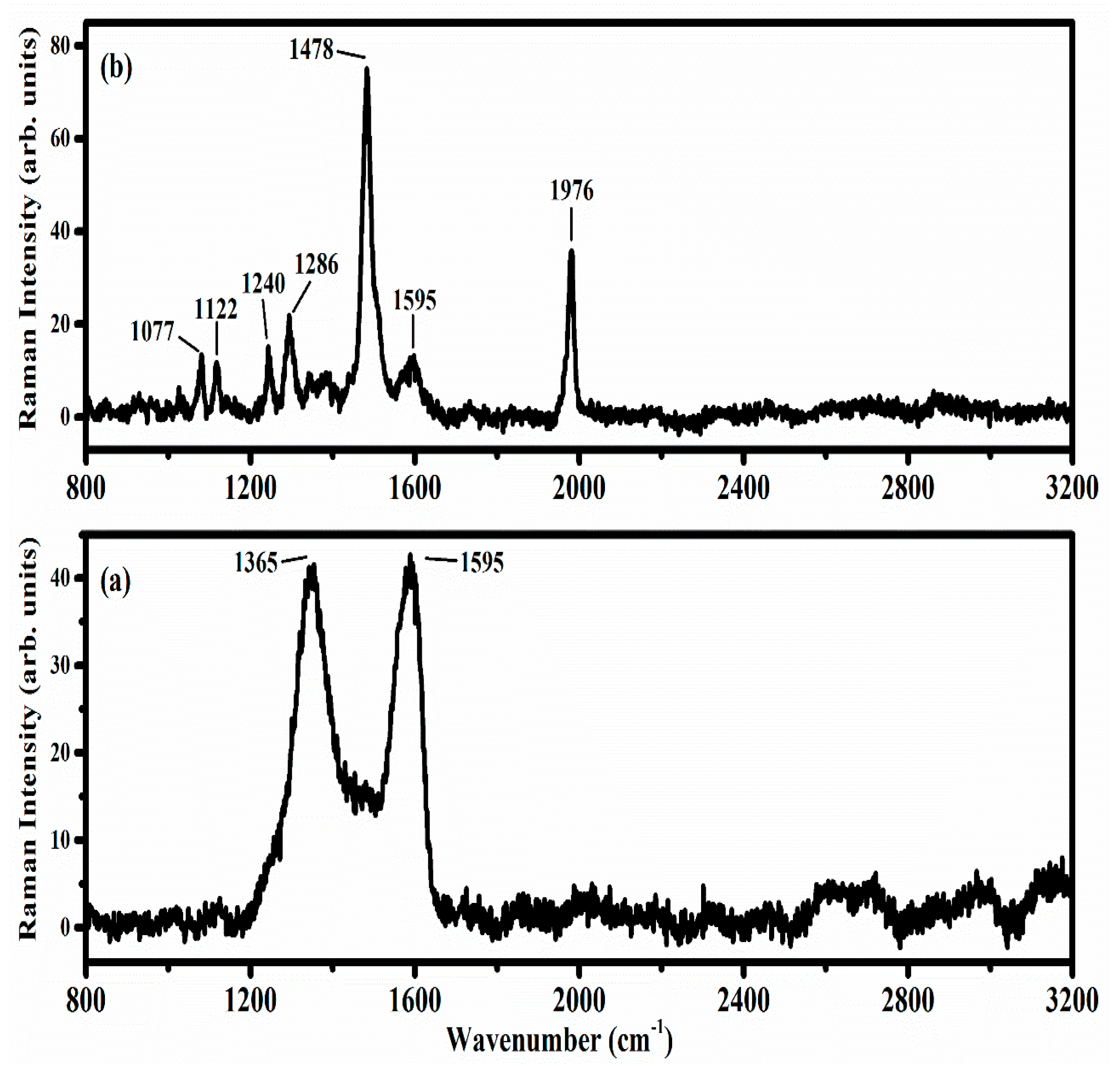
The Ag/GO/Au sandwich structure is an interesting configuration that combines silver, GO, and gold.
For reference, Figure 12a presents the illustrative Raman spectrum collected from a thin GO film (8 nm) dip-coated onto an untreated glass substrate. This measurement was conducted using low laser intensity (OD2).
The characteristic traits of GO, represented by the D and G bands, become noticeable at approximately 1365 cm−1 and 1595 cm−1, respectively. On the contrary, the spectrum derived from the Ag/GO/Au sandwich structure displays a markedly different profile, featuring several pronounced peaks that exceed the expected intensity levels of the GO bands previously described in the reference spectrum. This unique spectral behavior is often observed in areas of the sample that appear darker under microscopic examination, generally indicative of the presence of multiple GO layers.
Figure 12b illustrates a Raman spectrum acquired from a “dark” region within the Ag/GO/Au sandwich structure. A low laser intensity setting (OD2) was used to highlight this particular spectral behavior. Although the D and G bands typical of GO are clearly visible at approximately 1365 cm−1 and 1595 cm−1, similar to the reference spectrum in Figure 12a, the most notable observation is the appearance of multiple additional peaks with sharp definitions. In some cases, these peaks are strikingly prominent, displaying an even higher intensity than the GO bands.
The most noticeable peaks are found at 1077 cm−1, 1122 cm−1, 1240 cm−1, 1286 cm−1, 1478 cm−1, and 1976 cm−1. These distinctly sharp peaks are linked to localized vibrational modes of molecular groups that attach themselves to the GO network and establish a close interaction with metal particles or protrusions, commonly referred to as “hot spots.”
These supplementary Raman modes exhibit instability under heat treatment. Specifically, under high laser intensities, the pronounced peaks associated with the “hot spots” disappear, making the resulting Raman spectrum closely align with that shown in Figure 12a. This change mainly shows the disordered features of the GO network. The disappearance of these peaks can be understood as the result of either photolysis or thermolysis affecting the molecular groups that were amplifying the Raman signals at the “hot spots”. Despite the higher laser power, the fundamental carbon structure of GO remains unaffected.
6. Conclusions, Applications, and Outlook
6.1. Conclusions
This review outlines our recent research on graphene and other 2D materials, focusing on the use of micro-Raman spectroscopy for characterization. Among the key findings:
- GO Thin Films on Ti/Glass Substrates: We used micro-Raman spectroscopy to study the properties of GO layers that were deposited on titanium substrates through electrophoretic deposition. This technique proved invaluable for gaining insights into the structural and optical characteristics of the GO layers.
- GO Thin Films on Magnetron-Sputtered Silver: A significant portion of the review is dedicated to the study of GO thin films fabricated by dip-coating onto magnetron-sputtered silver substrates. Micro-Raman analysis reveals that these films exhibit SERS activity.
- Optical Properties of MoS2: This review also includes an exploration of the optical properties of solution-based MoS2, with micro-Raman spectroscopy employed for its characterization.
- Investigation of GNPs: This review includes a section on the investigation of GNPs.
- Monolayer Graphene on SiO2/Si Substrates: The optical properties of monolayer graphene samples grown via CVD on SiO2/Si substrates are discussed.
- Silver/GO/Gold Sandwich Structure: The review reports on the micro-Raman investigation of a silver/GO/gold sandwich structure. Notably, sharp Raman modes have been observed, sometimes even exhibiting greater intensity than typical GO bands, particularly under low laser power conditions.
6.2. Applications of Graphene and Other Two-Dimensional Materials
Raman spectroscopy is a critical tool for characterizing the properties of graphene, especially in the development of graphene-based field-effect transistors (FETs). By identifying the doping levels, Raman spectroscopy enables the fine-tuning of the electronic properties of these transistors, directly affecting their speed and energy efficiency. Additionally, the technique provides valuable data on heat generation and dissipation within the FETs, contributing to their long-term stability and performance [92,93,94,95].
The technique also plays a significant role in advancing energy storage devices. Specifically, it helps researchers understand the distortion of electrode material during charge and discharge processes. This understanding is vital for enhancing both the efficiency and longevity of batteries and other energy storage systems based on graphene [96].
In optoelectronic applications like solar cells and organic light-emitting diodes (OLEDs) [97], graphene’s high optical transparency, electrical conductivity, and mechanical flexibility make it a material of choice. Raman spectroscopy aids in the identification of interlayer coupling and the number of graphene layers in these devices, which is crucial for optimizing their performance.
Moreover, in nanoelectromechanical systems (NEMS), the technique is used to probe the local stress within multilayer graphene cantilevers [98].
Raman spectroscopy is also instrumental in the study of van der Waals 2D heterostructure devices, such as those combining graphene and MoS2 [99]. The method allows for the in situ examination of charge transfer within these heterostructures, providing essential insights into the electronic interplay between the various layers.
While the applications of Raman spectroscopy in areas like FETs, energy storage, and optoelectronics are well-established, its potential in sensing technologies is gaining increasing attention [100].
It is worth noting that MoS2, a prominent member of the transition metal dichalcogenides family, has demonstrated significant applicability across various technological domains. Notably, MoS2 has been studied for its role as a spin-valley filter, as outlined in [101]. Additionally, its intrinsic optoelectronic characteristics make it suitable for phototransistor devices, as detailed in [102]. MoS2 has also been explored for its potential in rectifying contacts, as reported in [103], and in tunneling field-effect transistors, as described in [104].
The study of transition metal dichalcogenide monolayers (MX2), including MoS2, has revealed the importance of metal-induced gap states (MIGS) in spin-valley filters [101]. These MIGS are predicted to mediate valley- and spin-resolved charge transport near the ideal electrode/MX2 interface, thus initiating filtering. This insight is particularly crucial when the channel length is diminished as MIGS begin to govern the overall valley-spin transport in the tunneling regime. The findings offer design guidelines for efficient valley-spin filter devices, which could revolutionize information processing technologies.
In addition to its role in valley-spin filtering, MoS2 has been extensively studied for its intrinsic optoelectronic characteristics [102]. Raman spectroscopy serves as a vital tool for understanding these properties, especially when MoS2 is integrated into functional devices like phototransistors. Utilizing a fully transparent van der Waals heterostructure, researchers have been able to reveal the intrinsic photoresponsivity characteristics of monolayer MoS2, including its internal responsivity and quantum efficiency.
Similarly, transition metal dichalcogenides (TMDs), particularly MoS2, have garnered attention for their semiconducting applications at the nanoscale. These materials exhibit direct band gaps and high charge mobilities, making them ideal for use in nanoscale devices. One of the critical aspects of TMDs is the understanding of Schottky barrier heights (SBHs) [103], which are crucial for efficient charge injection into these semiconductors. These theoretical models help in estimating the charge neutrality levels and canonical Schottky barrier heights, which are pivotal for the device’s performance.
Further exploring the potential of MoS2, tunneling field-effect transistors (TFETs) using monolayer MoS2 as the channel have emerged as promising contenders for low-energy electronics. These MoS2-TFETs [104] are compatible with silicon CMOS technology and exhibit a lower off-state leakage current and subthreshold swing compared to traditional MOSFETs.
6.3. Outlook
Future research on GO and RGO should focus on gaining a deeper understanding of the reduction mechanisms, as well as developing strategies to control both the oxidation of graphite and its subsequent reduction. After producing RGO, it can be chemically functionalized or paired with other 2D materials to tailor its properties for specialized commercial uses. For instance, the fabrication of nanocomposites, including RGO and TMDs, such as MoS2, holds promise for supercapacitor applications.
Moreover, one of the critical areas requiring more in-depth study is the understanding of strain in graphene [105], especially when grown on transition metals via CVD or when mechanically transferred in the case of exfoliated graphene. The methods used for deposition or synthesis can have a significant impact on how graphene interacts with its substrate. Therefore, future studies should aim to establish a connection between the strength of this interaction and the thermal evolution of graphene’s Raman spectra. Although some efforts have been made to correlate strain with structural features, such as surface morphology, additional research is needed to establish connections between the strain and graphene’s electrical, optical, and thermal properties. Since doping has an impact on the strain in thin films, more research is also essential to explore its specific effects on the strain in graphene films.
Author Contributions
Writing—original draft preparation, G.G.P. and C.V.; writing—review and editing, G.G.P. and C.V.; supervision, C.V. All authors have read and agreed to the published version of the manuscript.
Funding
This research received no external funding.
Data Availability Statement
Not applicable.
Conflicts of Interest
The authors declare no conflict of interest.
References
- Ding, H.; Zhang, X. Sodium Intercalation in Nitrogen-Doped Graphene-Based Anode: A First-Principles Study. Crystals 2023, 13, 1011. [Google Scholar] [CrossRef]
- Sultana, S.M.N.; Helal, E.; Gutiérrez, G.; David, E.; Moghimian, N.; Demarquette, N.R. Effect of Few-Layer Graphene on the Properties of Mixed Polyolefin Waste Stream. Crystals 2023, 13, 358. [Google Scholar] [CrossRef]
- Sartanavičius, A.; Žemgulytė, J.; Ragulis, P.; Ratautas, K.; Trusovas, R. Laser-Induced Graphene in Polyimide for Antenna Applications. Crystals 2023, 13, 1003. [Google Scholar] [CrossRef]
- Zhu, C.; Lin, Z.; Zhang, D.; Shi, J.; Peng, S.; Jin, Z. Predicting the Level of Background Current Noise in Graphene Biosensor through a Non-Covalent Functionalization Process. Crystals 2023, 13, 359. [Google Scholar] [CrossRef]
- Le, H.C.; Pham, N.T.; Vu, D.C.; Pham, D.L.; Nguyen, S.H.; Nguyen, T.T.; Nguyen, C.D. Nitrogen-Doped Graphene Quantum Dot–Tin Dioxide Nanocomposite Ultrathin Films as Efficient Electron Transport Layers for Planar Perovskite Solar Cells. Crystals 2023, 13, 961. [Google Scholar] [CrossRef]
- Wang, Y.; Zou, B.; Rente, B.; Alford, N.; Petrov, P.K. Deposition of Nanocrystalline Multilayer Graphene Using Pulsed Laser Deposition. Crystals 2023, 13, 881. [Google Scholar] [CrossRef]
- Hui, Y.; Zu, H.; Song, R.; Fu, H.; Luo, K.; Tian, C.; Wu, B.; Huang, G.-L.; Kou, Z.; Cheng, X.; et al. Graphene-Assembled Film-Based Reconfigurable Filtering Antenna with Enhanced Corrosion-Resistance. Crystals 2023, 13, 747. [Google Scholar] [CrossRef]
- Jibin, K.P.; Augustine, S.; Velayudhan, P.; George, J.S.; Krishnageham Sidharthan, S.; Poulose, S.V.; Thomas, S. Unleashing the Power of Graphene-Based Nanomaterials for Chromium(VI) Ion Elimination from Water. Crystals 2023, 13, 1047. [Google Scholar] [CrossRef]
- Bhuyan, M.S.A.; Uddin, M.N.; Islam, M.M.; Bipasha, F.A.; Hossain, S.S. Synthesis of graphene. Int. Nano Lett. 2016, 6, 65–83. [Google Scholar] [CrossRef]
- Randviir, E.P.; Brownson, D.A.C.; Banks, C.E. A decade of graphene research: Production, applications and outlook. Mater. Today 2014, 17, 426–432. [Google Scholar] [CrossRef]
- Huang, X.; Qi, X.; Boey, F.; Zhang, H. Graphene-based composites. Chem. Soc. Rev. 2012, 41, 666–686. [Google Scholar] [CrossRef] [PubMed]
- Berry, V. Impermeability of graphene and its applications. Carbon N. Y. 2013, 62, 1–10. [Google Scholar] [CrossRef]
- Novoselov, K.S.; Fal′ko, V.I.; Colombo, L.; Gellert, P.R.; Schwab, M.G.; Kim, K. A roadmap for graphene. Nature 2012, 490, 192–200. [Google Scholar] [CrossRef]
- Rao, C.N.R.; Biswas, K.; Subrahmanyam, K.S.; Govindaraj, A. Graphene, the new nanocarbon. J. Mater. Chem. 2009, 19, 2457–2469. [Google Scholar] [CrossRef]
- Stoller, M.D.; Park, S.; Zhu, Y.; An, J.; Ruoff, R.S. Graphene-Based Ultracapacitors. Nano Lett. 2008, 8, 3498–3502. [Google Scholar] [CrossRef] [PubMed]
- Lui, C.H.; Liu, L.; Mak, K.F.; Flynn, G.W.; Heinz, T.F. Ultraflat graphene. Nature 2009, 462, 339–341. [Google Scholar] [CrossRef]
- Bai, J.; Zhong, X.; Jiang, S.; Huang, Y.; Duan, X. Graphene nanomesh. Nat. Nanotechnol. 2010, 5, 190–194. [Google Scholar] [CrossRef]
- Obraztsova, E.D.; Rybin, M.G.; Obraztsov, P.A. 7—Optical properties of graphene. In Woodhead Publishing Series in Electronic and Optical Materials; Skakalova, V., Kaiser, A.B.B.T.-G., Eds.; Woodhead Publishing: Sawston, UK, 2021; pp. 133–142. ISBN 978-0-08-102848-3. [Google Scholar] [CrossRef]
- Jafari, B.; Gholizadeh, E.; Golmohammadi, S.; Ebadzadeh, M.; Soofi, H.; Aghili, S. An Innovative method for adjustable broadband THz to Mid-IR optical modulator using Graphene Gratings surface plasmon Fabry–Perot resonances with low insertion loss, high speed and modulation depth. Opt. Commun. 2023, 530, 129200. [Google Scholar] [CrossRef]
- Rogalski, A. Graphene-based materials in the infrared and terahertz detector families: A tutorial. Adv. Opt. Photonics 2019, 11, 314–379. [Google Scholar] [CrossRef]
- Mbayachi, V.B.; Ndayiragije, E.; Sammani, T.; Taj, S.; Mbuta, E.R.; Khan, A. ullah Graphene synthesis, characterization and its applications: A review. Results Chem. 2021, 3, 100163. [Google Scholar] [CrossRef]
- Chen, X.; Zhang, L.; Chen, S. Large area CVD growth of graphene. Synth. Met. 2015, 210, 95–108. [Google Scholar] [CrossRef]
- Shafi, M.; Duan, P.; Liu, W.; Zhang, W.; Zhang, C.; Hu, X.; Zha, Z.; Liu, R.; Liu, C.; Jiang, S.; et al. SERS Sensing Using Graphene-Covered Silver Nanoparticles and Metamaterials for the Detection of Thiram in Soil. Langmuir 2022, 38, 16183–16193. [Google Scholar] [CrossRef] [PubMed]
- Cao, S.; Wang, T.; Sun, Q.; Tang, Y.; Hu, B.; Levy, U.; Yu, W. Graphene–Silver Hybrid Metamaterial for Tunable and High Absorption at Mid-Infrared Waveband. IEEE Photonics Technol. Lett. 2018, 30, 475–478. [Google Scholar] [CrossRef]
- Shaban, N.; Prajapati, Y.K.; Mohammadkhani, R. Performance enhancement of waveguide-coupled and metamaterial surface plasmon resonance sensors based on silver-bismuth ferrite and graphene. J. Mater. Sci. Mater. Electron. 2023, 34, 309. [Google Scholar] [CrossRef]
- Kaushik, V.; Kagdada, H.L.; Singh, D.K.; Pathak, S. Enhancement of SERS effect in Graphene-Silver hybrids. Appl. Surf. Sci. 2022, 574, 151724. [Google Scholar] [CrossRef]
- Yu, X.; Cai, H.; Zhang, W.; Li, X.; Pan, N.; Luo, Y.; Wang, X.; Hou, J.G. Tuning Chemical Enhancement of SERS by Controlling the Chemical Reduction of Graphene Oxide Nanosheets. ACS Nano 2011, 5, 952–958. [Google Scholar] [CrossRef]
- Zhang, J.; Yang, H.; Shen, G.; Cheng, P.; Zhang, J.; Guo, S. Reduction of graphene oxide via L-ascorbic acid. Chem. Commun. 2010, 46, 1112–1114. [Google Scholar] [CrossRef]
- Huq, T.; Ong, H.C.; Chew, B.T.; Leong, K.Y.; Kazi, S.N. Review on aqueous graphene nanoplatelet Nanofluids: Preparation, Stability, thermophysical Properties, and applications in heat exchangers and solar thermal collectors. Appl. Therm. Eng. 2022, 210, 118342. [Google Scholar] [CrossRef]
- Ajala, O.J.; Tijani, J.O.; Bankole, M.T.; Abdulkareem, A.S. A critical review on graphene oxide nanostructured material: Properties, Synthesis, characterization and application in water and wastewater treatment. Environ. Nanotechnol. Monit. Manag. 2022, 18, 100673. [Google Scholar] [CrossRef]
- Razaq, A.; Bibi, F.; Zheng, X.; Papadakis, R.; Jafri, S.H.; Li, H. Review on Graphene-, Graphene Oxide-, Reduced Graphene Oxide-Based Flexible Composites: From Fabrication to Applications. Materials 2022, 15, 1012. [Google Scholar] [CrossRef]
- Chen, D.; Feng, H.; Li, J. Graphene oxide: Preparation, functionalization, and electrochemical applications. Chem. Rev. 2012, 112, 6027–6053. [Google Scholar] [CrossRef]
- Yang, Q.-D.; Li, J.; Cheng, Y.; Li, H.-W.; Guan, Z.; Yu, B.; Tsang, S.-W. Graphene oxide as an efficient hole-transporting material for high-performance perovskite solar cells with enhanced stability. J. Mater. Chem. A 2017, 5, 9852–9858. [Google Scholar] [CrossRef]
- De Silva, K.K.H.; Huang, H.-H.; Joshi, R.K.; Yoshimura, M. Chemical reduction of graphene oxide using green reductants. Carbon N. Y. 2017, 119, 190–199. [Google Scholar] [CrossRef]
- Yee, K.; Ghayesh, M.H. A review on the mechanics of graphene nanoplatelets reinforced structures. Int. J. Eng. Sci. 2023, 186, 103831. [Google Scholar] [CrossRef]
- Moosa, A.; Ramazani, S.A.A.; Ibrahim, M. Mechanical and Electrical Properties of Graphene Nanoplates and Carbon-Nanotubes Hybrid Epoxy Nanocomposites. Am. J. Mater. Sci. 2016, 6, 157–165. [Google Scholar] [CrossRef]
- Kumar, D.; Singh, K.; Verma, V.; Bhatti, H.S. Microwave assisted synthesis and characterization of graphene nanoplatelets. Appl. Nanosci. 2016, 6, 97–103. [Google Scholar] [CrossRef]
- Krittayavathananon, A.; Li, X.; Batchelor-McAuley, C.; Sawangphruk, M.; Compton, R.G. Comparing the effect of different surfactants on the aggregation and electrical contact properties of graphene nanoplatelets. Appl. Mater. Today 2018, 12, 163–167. [Google Scholar] [CrossRef]
- Moriche, R.; Jiménez-Suárez, A.; Sánchez, M.; Prolongo, S.G.; Ureña, A. High sensitive damage sensors based on the use of functionalized graphene nanoplatelets coated fabrics as reinforcement in multiscale composite materials. Compos. Part B Eng. 2018, 149, 31–37. [Google Scholar] [CrossRef]
- Manzeli, S.; Ovchinnikov, D.; Pasquier, D.; Yazyev, O.V.; Kis, A. 2D transition metal dichalcogenides. Nat. Rev. Mater. 2017, 2, 17033. [Google Scholar] [CrossRef]
- Han, S.A.; Bhatia, R.; Kim, S.-W. Synthesis, properties and potential applications of two-dimensional transition metal dichalcogenides. Nano Converg. 2015, 2, 17. [Google Scholar] [CrossRef]
- Babu, G.; Masurkar, N.; Al Salem, H.; Arava, L.M.R. Transition Metal Dichalcogenide Atomic Layers for Lithium Polysulfides Electrocatalysis. J. Am. Chem. Soc. 2017, 139, 171–178. [Google Scholar] [CrossRef] [PubMed]
- Chen, B.; Chao, D.; Liu, E.; Jaroniec, M.; Zhao, N.; Qiao, S.-Z. Transition metal dichalcogenides for alkali metal ion batteries: Engineering strategies at the atomic level. Energy Environ. Sci. 2020, 13, 1096–1131. [Google Scholar] [CrossRef]
- Politano, G.G.; Versace, C.; Vena, C.; Castriota, M.; Ciuchi, F.; Fasanella, A.; Desiderio, G.; Cazzanelli, E. Physical investigation of electrophoretically deposited graphene oxide and reduced graphene oxide thin films. J. Appl. Phys. 2016, 120, 195307. [Google Scholar] [CrossRef]
- Politano, G.G.; Cazzanelli, E.; Versace, C.; Vena, C.; De Santo, M.P.; Castriota, M.; Ciuchi, F.; Bartolino, R. Graphene oxide on magnetron sputtered silver thin films for SERS and metamaterial applications. Appl. Surf. Sci. 2018, 427, 927–933. [Google Scholar] [CrossRef]
- Politano, G.G.; Cazzanelli, E.; Versace, C.; Castriota, M.; Desiderio, G.; Davoli, M.; Vena, C.; Bartolino, R. Micro-Raman investigation of Ag/graphene oxide/Au sandwich structure. Mater. Res. Express 2019, 6, 075605. [Google Scholar] [CrossRef]
- Politano, G.G.; Nucera, A.; Castriota, M.; Desiderio, G.; Vena, C.; Versace, C. Spectroscopic and morphological study of graphene nanoplatelets thin films on Si/SiO2 substrates. Mater. Res. Express 2019, 6, 106432. [Google Scholar] [CrossRef]
- Politano, G.G.; Castriota, M.; De Santo, M.P.; Pipita, M.M.; Desiderio, G.; Vena, C.; Versace, C. Variable angle spectroscopic ellipsometry characterization of spin-coated MoS2 films. Vacuum 2021, 189, 110232. [Google Scholar] [CrossRef]
- Castriota, M.; Politano, G.G.; Vena, C.; De Santo, M.P.; Desiderio, G.; Davoli, M.; Cazzanelli, E.; Versace, C. Variable Angle Spectroscopic Ellipsometry investigation of CVD-grown monolayer graphene. Appl. Surf. Sci. 2019, 467–468, 213–220. [Google Scholar] [CrossRef]
- Bruna, M.; Ott, A.K.; Ijäs, M.; Yoon, D.; Sassi, U.; Ferrari, A.C. Doping Dependence of the Raman Spectrum of Defected Graphene. ACS Nano 2014, 8, 7432–7441. [Google Scholar] [CrossRef]
- Bonaccorso, F.; Sun, Z.; Hasan, T.; Ferrari, A.C. Graphene photonics and optoelectronics. Nat. Photonics 2010, 4, 611. [Google Scholar] [CrossRef]
- Katsnelson, M.I. Graphene: Carbon in two dimensions. Mater Today 2007, 10, 20. [Google Scholar] [CrossRef]
- Fang, W.; Song, Y.; Hsu, A.L.; Kong, J. A review of large-area bilayer graphene synthesis by chemical vapor deposition. Nanoscale 2015, 7, 20335. [Google Scholar] [CrossRef]
- Yu, X.Z.; Hwang, C.G.; Jozwiak, C.M.; Köhl, A.; Schmid, A.K.; Lanzara, A. New synthesis method for the growth of epitaxial graphene. J. Electron Spectros. Relat. Phenomena 2011, 184, 100–106. [Google Scholar] [CrossRef]
- Sinclair, R.C.; Suter, J.L.; Coveney, P. V Micromechanical exfoliation of graphene on the atomistic scale. Phys. Chem. Chem. Phys. 2019, 21, 5716–5722. [Google Scholar] [CrossRef]
- Mishra, N.; Boeckl, J.; Motta, N.; Iacopi, F. Graphene growth on silicon carbide: A review. Phys. Status Solidi 2016, 213, 2277–2289. [Google Scholar] [CrossRef]
- Thakur, S.; Karak, N. Alternative methods and nature-based reagents for the reduction of graphene oxide: A review. Carbon N. Y. 2015, 94, 224–242. [Google Scholar] [CrossRef]
- Pei, S.; Cheng, H.-M. The reduction of graphene oxide. Carbon N. Y. 2012, 50, 3210–3228. [Google Scholar] [CrossRef]
- Boukhvalov, D.W.; Katsnelson, M.I. Modeling of Graphite Oxide. J. Am. Chem. Soc. 2008, 130, 10697–10701. [Google Scholar] [CrossRef] [PubMed]
- Nakajima, T.; Matsuo, Y. Formation process and structure of graphite oxide. Carbon N. Y. 1994, 32, 469–475. [Google Scholar] [CrossRef]
- Smirnov, V.A.; Arbuzov, A.A.; Shul’ga, Y.M.; Baskakov, S.A.; Martynenko, V.M.; Muradyan, V.E.; Kresova, E.I. Photoreduction of graphite oxide. High Energy Chem. 2011, 45, 57–61. [Google Scholar] [CrossRef]
- Petridis, L.V.; Kokkinos, N.C.; Mitropoulos, A.C.; Kyzas, G.Z. Chapter 8—Graphene aerogels for oil absorption. In Advanced Low-Cost Separation Techniques in Interface Science; Kyzas, G.Z., Mitropoulos, A.C., Eds.; Elsevier: Amsterdam, The Netherlands, 2019; Volume 30, pp. 173–197. ISBN 1573-4285. [Google Scholar] [CrossRef]
- Konkena, B.; Vasudevan, S. Understanding Aqueous Dispersibility of Graphene Oxide and Reduced Graphene Oxide through pKa Measurements. J. Phys. Chem. Lett. 2012, 3, 867–872. [Google Scholar] [CrossRef] [PubMed]
- Paredes, J.I.; Villar-Rodil, S.; Martínez-Alonso, A.; Tascón, J.M.D. Graphene Oxide Dispersions in Organic Solvents. Langmuir 2008, 24, 10560–10564. [Google Scholar] [CrossRef] [PubMed]
- Yu, H.; Zhang, B.; Bulin, C.; Li, R.; Xing, R. High-efficient Synthesis of Graphene Oxide Based on Improved Hummers Method. Sci. Rep. 2016, 6, 36143. [Google Scholar] [CrossRef] [PubMed]
- Dreyer, D.R.; Park, S.; Bielawski, C.W.; Ruoff, R.S. The chemistry of graphene oxide. Chem. Soc. Rev. 2010, 39, 228–240. [Google Scholar] [CrossRef]
- Kwon, S.; Lee, K.E.; Lee, H.; Koh, S.J.; Ko, J.-H.; Kim, Y.-H.; Kim, S.O.; Park, J.Y. The Effect of Thickness and Chemical Reduction of Graphene Oxide on Nanoscale Friction. J. Phys. Chem. B 2018, 122, 543–547. [Google Scholar] [CrossRef]
- Zhao, C.; Xing, L.; Xiang, J.; Cui, L.; Jiao, J.; Sai, H.; Li, Z.; Li, F. Formation of uniform reduced graphene oxide films on modified PET substrates using drop-casting method. Particuology 2014, 17, 66–73. [Google Scholar] [CrossRef]
- Sun, H.B.; Yang, J.; Zhou, Y.Z.; Zhao, N.; Li, D. Preparation of reduced graphene oxide films by dip coating technique and their electrical conductivity. Mater. Technol. 2014, 29, 14–20. [Google Scholar] [CrossRef]
- Nasiłowska, B.; Bogdanowicz, Z.; Hińcza, K.; Mierczyk, Z.; Góźdź, S.; Djas, M.; Kowiorski, K.; Bombalska, A.; Kowalik, A. Graphene Oxide Aerosol Deposition and its Influence on Cancer Cells. Preliminary Results. Materials 2020, 13, 4464. [Google Scholar] [CrossRef]
- Komarov, I.A.; Danilova, E.A.; Denisenko, E.I.; Peretiyagin, V.G.; Rabchinskii, M.K. Spin-coating deposition of graphene oxide from mixed water-organic suspensions. Fuller. Nanotub. Carbon Nanostruct. 2022, 30, 146–151. [Google Scholar] [CrossRef]
- Marcin Behunová, D.; Gallios, G.; Girman, V.; Kolev, H.; Kaňuchová, M.; Dolinská, S.; Václavíková, M. Electrophoretic Deposition of Graphene Oxide on Stainless Steel Substrate. Nanomaterials 2021, 11, 1779. [Google Scholar] [CrossRef]
- Li, X.; Shen, Q.; Zhang, Y.; Wang, L.; Nie, C. Wear behavior of electrodeposited nickel/graphene composite coating. Diam. Relat. Mater. 2021, 119, 108589. [Google Scholar] [CrossRef]
- Tseluikin, V.; Dzhumieva, A.; Tikhonov, D.; Yakovlev, A.; Strilets, A.; Tribis, A.; Lopukhova, M. Pulsed Electrodeposition and Properties of Nickel-Based Composite Coatings Modified with Graphene Oxide. Coatings 2022, 12, 656. [Google Scholar] [CrossRef]
- Ray, S.C. Applications of Graphene and Graphene-Oxide based Nanomaterials. In Applications of Graphene and Graphene-Oxide Based Nanomaterials; Elsevier: Amsterdam, The Netherlands, 2015; pp. 1–84. [Google Scholar]
- Tkachev, S.V.; Buslaeva, E.Y.; Naumkin, A.V.; Kotova, S.L.; Laure, I.V.; Gubin, S.P. Reduced graphene oxide. Inorg. Mater. 2012, 48, 796–802. [Google Scholar] [CrossRef]
- Park, S.; An, J.; Potts, J.R.; Velamakanni, A.; Murali, S.; Ruoff, R.S. Hydrazine-reduction of graphite-and graphene oxide. Carbon N. Y. 2011, 49, 3019–3023. [Google Scholar] [CrossRef]
- Fernández-Merino, M.J.; Guardia, L.; Paredes, J.I.; Villar-Rodil, S.; Solís-Fernández, P.; Martínez-Alonso, A.; Tascón, J.M.D. Vitamin C Is an Ideal Substitute for Hydrazine in the Reduction of Graphene Oxide Suspensions. J. Phys. Chem. C 2010, 114, 6426–6432. [Google Scholar] [CrossRef]
- Jung, I.; Dikin, D.A.; Piner, R.D.; Ruoff, R.S. Tunable Electrical Conductivity of Individual Graphene Oxide Sheets Reduced at “Low” Temperatures. Nano Lett. 2008, 8, 4283–4287. [Google Scholar] [CrossRef]
- Stankovich, S.; Dikin, D.A.; Piner, R.D.; Kohlhaas, K.A.; Kleinhammes, A.; Jia, Y.; Wu, Y.; Nguyen, S.T.; Ruoff, R.S. Synthesis of graphene-based nanosheets via chemical reduction of exfoliated graphite oxide. Carbon N. Y. 2007, 45, 1558–1565. [Google Scholar] [CrossRef]
- Sadhukhan, S.; Ghosh, T.K.; Rana, D.; Roy, I.; Bhattacharyya, A.; Sarkar, G.; Chakraborty, M.; Chattopadhyay, D. Studies on synthesis of reduced graphene oxide (RGO) via green route and its electrical property. Mater. Res. Bull. 2016, 79, 41–51. [Google Scholar] [CrossRef]
- Chua, C.K.; Pumera, M. Chemical reduction of graphene oxide: A synthetic chemistry viewpoint. Chem. Soc. Rev. 2014, 43, 291–312. [Google Scholar] [CrossRef]
- Zhu, Y.; Murali, S.; Cai, W.; Li, X.; Suk, J.W.; Potts, J.R.; Ruoff, R.S. Graphene and graphene oxide: Synthesis, properties, and applications. Adv. Mater. 2010, 22, 3906–3924. [Google Scholar] [CrossRef]
- Ferrari, A.C. Raman spectroscopy of graphene and graphite: Disorder, electron–phonon coupling, doping and nonadiabatic effects. Solid State Commun. 2007, 143, 47–57. [Google Scholar] [CrossRef]
- Ferrari, A.C.; Meyer, J.C.; Scardaci, V.; Casiraghi, C.; Lazzeri, M.; Mauri, F.; Piscanec, S.; Jiang, D.; Novoselov, K.S.; Roth, S.; et al. Raman Spectrum of Graphene and Graphene Layers. Phys. Rev. Lett. 2006, 97, 187401. [Google Scholar] [CrossRef] [PubMed]
- Das, A.; Pisana, S.; Chakraborty, B.; Piscanec, S.; Saha, S.K.; Waghmare, U.V.; Novoselov, K.S.; Krishnamurthy, H.R.; Geim, A.K.; Ferrari, A.C.; et al. Monitoring dopants by Raman scattering in an electrochemically top-gated graphene transistor. Nat. Nanotechnol. 2008, 3, 210–215. [Google Scholar] [CrossRef]
- Sharma, N.; Tomar, S.; Shkir, M.; Kant Choubey, R.; Singh, A. Study of Optical and Electrical Properties of Graphene Oxide. Mater. Today Proc. 2021, 36, 730–735. [Google Scholar] [CrossRef]
- Wu, J.-B.; Lin, M.-L.; Cong, X.; Liu, H.-N.; Tan, P.-H. Raman spectroscopy of graphene-based materials and its applications in related devices. Chem. Soc. Rev. 2018, 47, 1822–1873. [Google Scholar] [CrossRef] [PubMed]
- De Silva, K.K.H.; Viswanath, P.; Rao, V.K.; Suzuki, S.; Yoshimura, M. New Insight into the Characterization of Graphene Oxide and Reduced Graphene Oxide Monolayer Flakes on Si-Based Substrates by Optical Microscopy and Raman Spectroscopy. J. Phys. Chem. C 2021, 125, 7791–7798. [Google Scholar] [CrossRef]
- Malard, L.M.; Pimenta, M.A.; Dresselhaus, G.; Dresselhaus, M.S. Raman spectroscopy in graphene. Phys. Rep. 2009, 473, 51–87. [Google Scholar] [CrossRef]
- Verde, M.; Peiteado, M.; Caballero, A.C.; Villegas, M.; Ferrari, B. Electrophoretic Deposition of Transparent ZnO Thin Films from Highly Stabilized Colloidal Suspensions. J. Colloid Interface Sci. 2012, 373, 27–33. [Google Scholar] [CrossRef]
- Yan, Y.; Peng, S.; Jin, Z.; Zhang, D.; Shi, J. Recovering the Intrinsic Electrical Property of a Graphene Field-Effect Transistor by Interface Cleaning Technology. ACS Appl. Electron. Mater. 2023, 5, 3113–3119. [Google Scholar] [CrossRef]
- Kim, S.; Kim, B.; Park, S.; Chang, W.S.; Kang, H.; Kim, S.; Lee, H.; Kim, S. Hysteretic behavior of all CVD h-BN/graphene/h-BN heterostructure field-effect transistors by interfacial charge trap. Surf. Interfaces 2023, 36, 102615. [Google Scholar] [CrossRef]
- Chaudhary, M.; Xin, C.; Hu, Z.; Zhang, D.; Radtke, G.; Xu, X.; Billot, L.; Tripon-Canseliet, C.; Chen, Z. Nitrogen-Doped Carbon Quantum Dots on Graphene for Field-Effect Transistor Optoelectronic Memories. Adv. Electron. Mater. 2023, 9, 2300159. [Google Scholar] [CrossRef]
- Khan, M.F.; Elahi, E.; Hassan, N.U.; Rehman, M.A.; Khalil, H.M.W.; Khan, M.A.; Rehman, S.; Hao, A.; Noh, H.; Khan, K.; et al. Bipolar Photoresponse of a Graphene Field-Effect Transistor Induced by Photochemical Reactions. ACS Appl. Electron. Mater. 2023. [Google Scholar] [CrossRef]
- Vignesh, G.; Devendran, P.; Nallamuthu, N.; Sudhahar, S.; Kumar, P.S.; Kumar, M.K. Effects of nitrogen, sulphur, and temperature treatments on the spectral, structural, and electrochemical characteristics of graphene oxide for energy storage applications. Carbon Trends 2023, 11, 100262. [Google Scholar] [CrossRef]
- Zhang, D.; Du, J.; Zhang, W.; Tong, B.; Sun, Y.; Zhao, T.-Y.; Ma, L.-P.; Sun, D.-M.; Cheng, H.-M.; Ren, W. Carrier Transport Regulation of Pixel Graphene Transparent Electrodes for Active-Matrix Organic Light-Emitting Diode Display. Small 2023, 2302920. [Google Scholar] [CrossRef] [PubMed]
- Fan, X.; Smith, A.D.; Forsberg, F.; Wagner, S.; Schröder, S.; Akbari, S.S.A.; Fischer, A.C.; Villanueva, L.G.; Östling, M.; Lemme, M.C.; et al. Manufacture and characterization of graphene membranes with suspended silicon proof masses for MEMS and NEMS applications. Microsyst. Nanoeng. 2020, 6, 17. [Google Scholar] [CrossRef] [PubMed]
- Zhang, M.; Han, N.; Zhang, J.; Wang, J.; Chen, X.; Zhao, J.; Gan, X. Emergent second-harmonic generation in van der Waals heterostructure of bilayer MoS2 and monolayer graphene. Sci. Adv. 2023, 9, eadf4571. [Google Scholar] [CrossRef]
- Thakkar, S.; De Luca, L.; Gaspa, S.; Mariani, A.; Garroni, S.; Iacomini, A.; Stagi, L.; Innocenzi, P.; Malfatti, L. Comparative Evaluation of Graphene Nanostructures in GERS Platforms for Pesticide Detection. ACS Omega 2022, 7, 5670–5678. [Google Scholar] [CrossRef]
- Szczęśniak, D.; Kais, S. Gap states and valley-spin filtering in transition metal dichalcogenide monolayers. Phys. Rev. B 2020, 101, 115423. [Google Scholar] [CrossRef]
- Pak, J.; Lee, I.; Cho, K.; Kim, J.-K.; Jeong, H.; Hwang, W.-T.; Ahn, G.H.; Kang, K.; Yu, W.J.; Javey, A.; et al. Intrinsic Optoelectronic Characteristics of MoS2 Phototransistors via a Fully Transparent van der Waals Heterostructure. ACS Nano 2019, 13, 9638–9646. [Google Scholar] [CrossRef]
- Szczęśniak, D.; Hoehn, R.D.; Kais, S. Canonical Schottky barrier heights of transition metal dichalcogenide monolayers in contact with a metal. Phys. Rev. B 2018, 97, 195315. [Google Scholar] [CrossRef]
- Lan, Y.-W.; Torres, C.M., Jr.; Tsai, S.-H.; Zhu, X.; Shi, Y.; Li, M.-Y.; Li, L.-J.; Yeh, W.-K.; Wang, K.L. Atomic-Monolayer MoS2 Band-to-Band Tunneling Field-Effect Transistor. Small 2016, 12, 5676–5683. [Google Scholar] [CrossRef] [PubMed]
- Ferralis, N. Probing Mechanical Properties of Graphene with Raman Spectroscopy. J. Mater. Sci. 2010, 45, 5135–5149. [Google Scholar] [CrossRef]
Figure 1.
Raman spectra of electrophoretically deposited graphene oxide on a titanium layer (a) prior to annealing and (b) after annealing at 400 °C. This content has been reproduced from reference [44] with permission granted by AIP Publishing. Copyright 2016, AIP Publishing.
Figure 1.
Raman spectra of electrophoretically deposited graphene oxide on a titanium layer (a) prior to annealing and (b) after annealing at 400 °C. This content has been reproduced from reference [44] with permission granted by AIP Publishing. Copyright 2016, AIP Publishing.
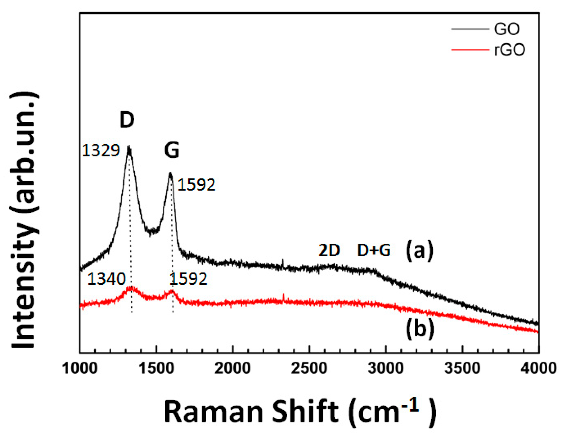
Figure 2.
Optical image of a representative area showing dip-coated graphene oxide films on a 10 nm magnetron-sputtered silver substrate. The laser highlights a “light” area. This content has been reproduced from reference Ref. [45] with permission granted by Elsevier. Copyright 2018, Elsevier.
Figure 2.
Optical image of a representative area showing dip-coated graphene oxide films on a 10 nm magnetron-sputtered silver substrate. The laser highlights a “light” area. This content has been reproduced from reference Ref. [45] with permission granted by Elsevier. Copyright 2018, Elsevier.
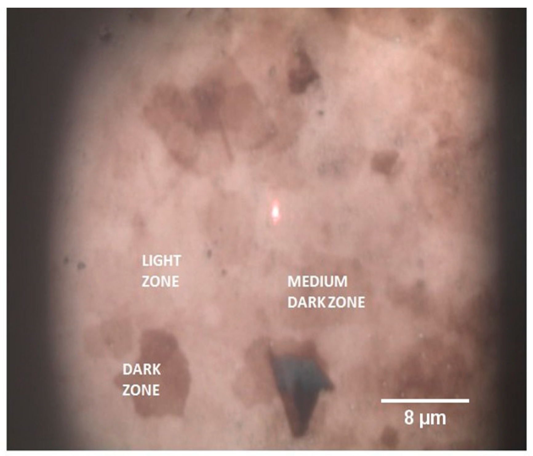
Figure 3.
Raman spectra of graphene oxide films dip-coated on bare glass at low laser intensity (OD2) (a) and graphene oxide films dip-coated on a 10 nm magnetron-sputtered silver/glass substrate at low laser intensity (OD2) (b). This content has been reproduced from reference Ref. [45] with permission granted by Elsevier. Copyright 2018, Elsevier.
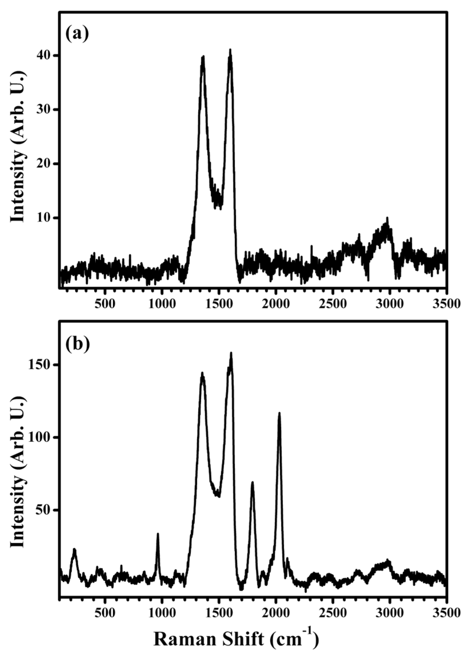
Figure 4.
Raman spectra of graphene oxide films fabricated via dip-coating on a 10 nm magnetron-sputtered silver/glass substrate under unfiltered full laser intensity. This content has been reproduced from Ref. [45] with permission granted by Elsevier. Copyright 2018, Elsevier.
Figure 4.
Raman spectra of graphene oxide films fabricated via dip-coating on a 10 nm magnetron-sputtered silver/glass substrate under unfiltered full laser intensity. This content has been reproduced from Ref. [45] with permission granted by Elsevier. Copyright 2018, Elsevier.
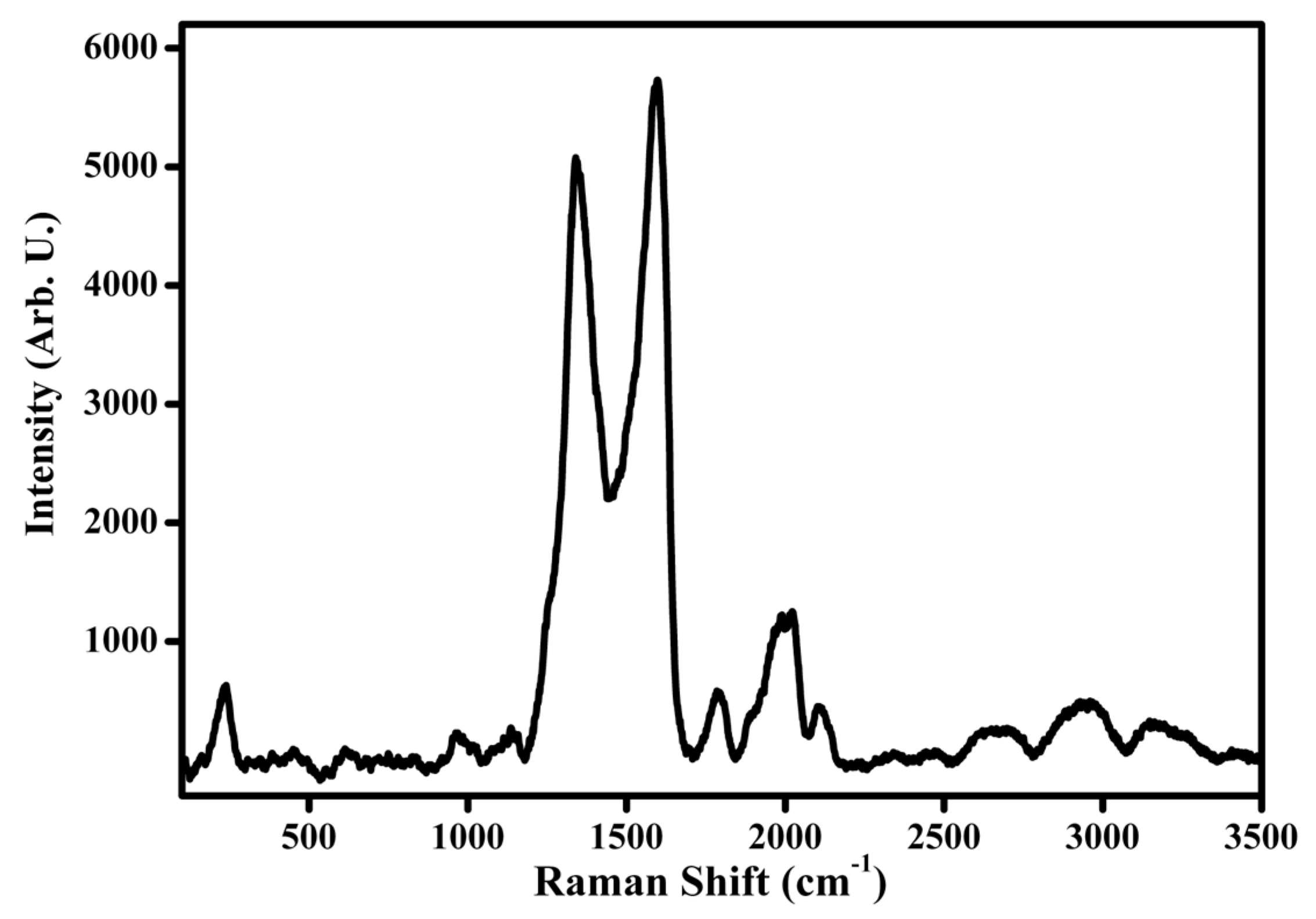
Figure 5.
Representative micro-Raman spectra collected from MoS2 films spin-coated onto Si/SiO2 substrates (a,b). This content has been reproduced from Ref. [48] with permission granted by Elsevier. Copyright 2021, Elsevier.
Figure 5.
Representative micro-Raman spectra collected from MoS2 films spin-coated onto Si/SiO2 substrates (a,b). This content has been reproduced from Ref. [48] with permission granted by Elsevier. Copyright 2021, Elsevier.
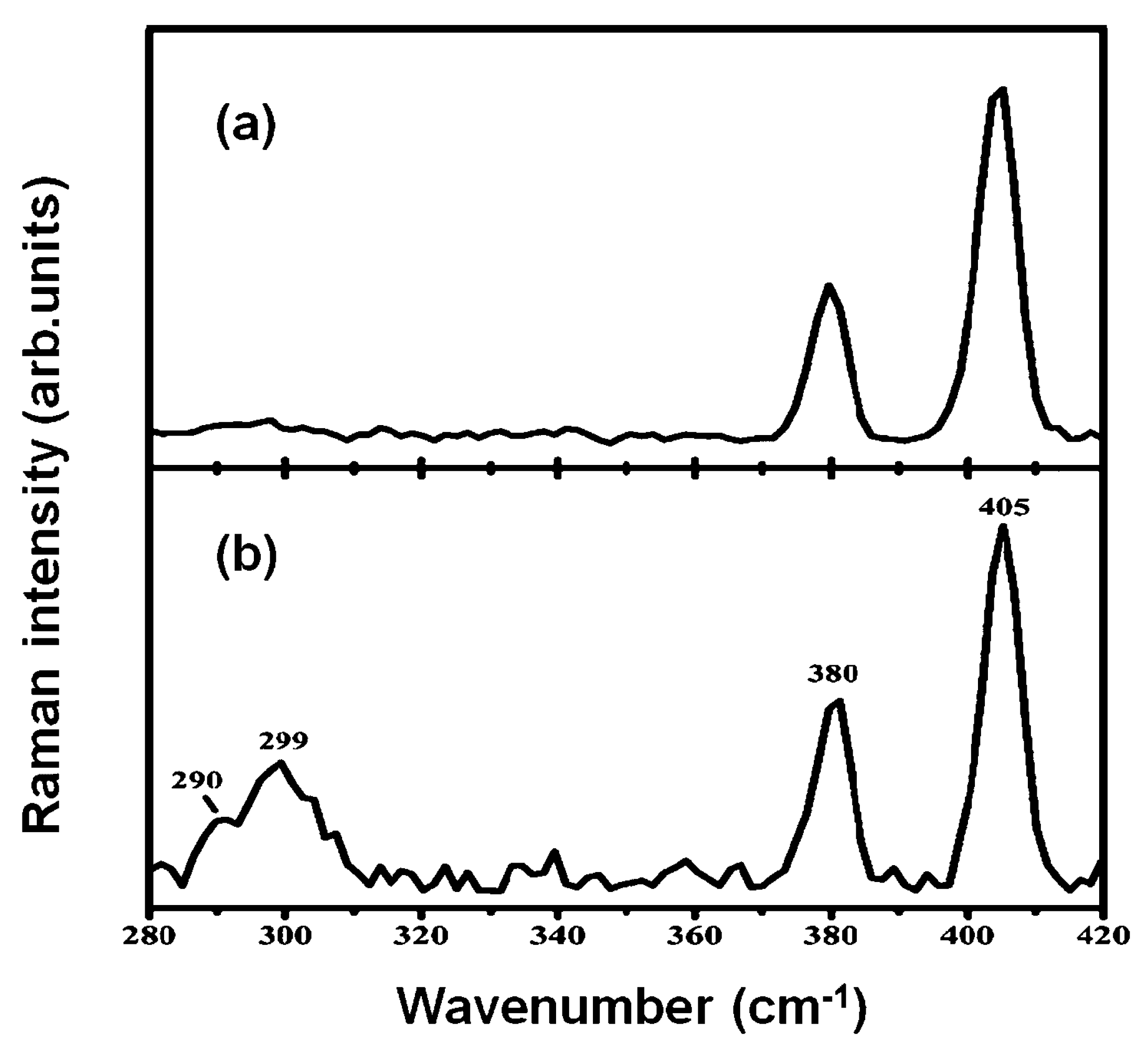
Figure 6.
Optical images depicting thin films of graphene nanoplatelets on Si/SiO2 (a–h). This content has been reproduced from Ref. [47] with permission granted by IOP Publishing. Copyright 2019, IOP Publishing.
Figure 6.
Optical images depicting thin films of graphene nanoplatelets on Si/SiO2 (a–h). This content has been reproduced from Ref. [47] with permission granted by IOP Publishing. Copyright 2019, IOP Publishing.

Figure 7.
Representative Raman spectrum acquired from the islands of graphene nanoplatelet thin films on Si/SiO2. This content has been reproduced from Ref. [47] with permission granted by IOP Publishing. Copyright 2019, IOP Publishing.
Figure 7.
Representative Raman spectrum acquired from the islands of graphene nanoplatelet thin films on Si/SiO2. This content has been reproduced from Ref. [47] with permission granted by IOP Publishing. Copyright 2019, IOP Publishing.
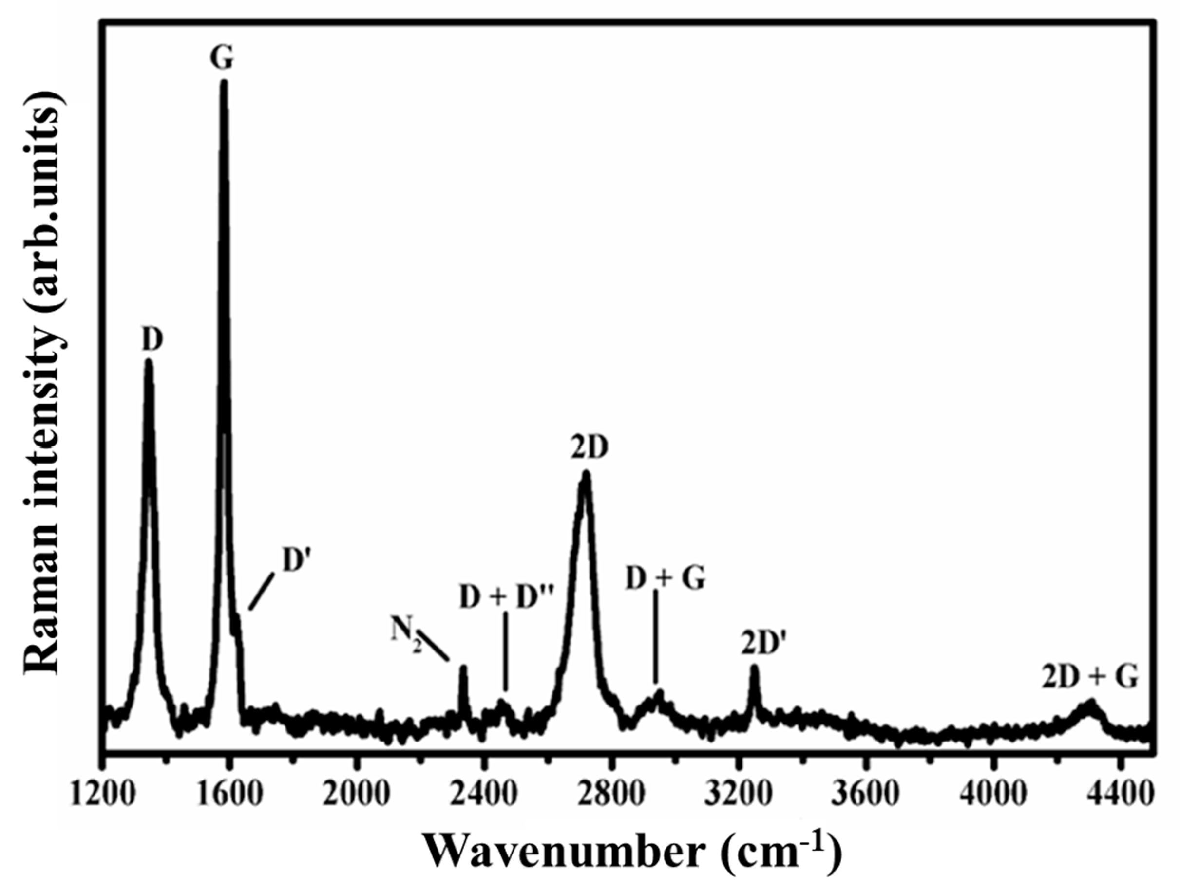
Figure 8.
Micrographs illustrating the central zone (A zone) and the border zone (B zone) of the sample. Darker regions and a brighter stripe are observed in the central zone (a), while a homogeneous region is visible in the border zone (b). This content has been reproduced from Ref. [49] with permission granted by Elsevier. Copyright 2019, Elsevier.
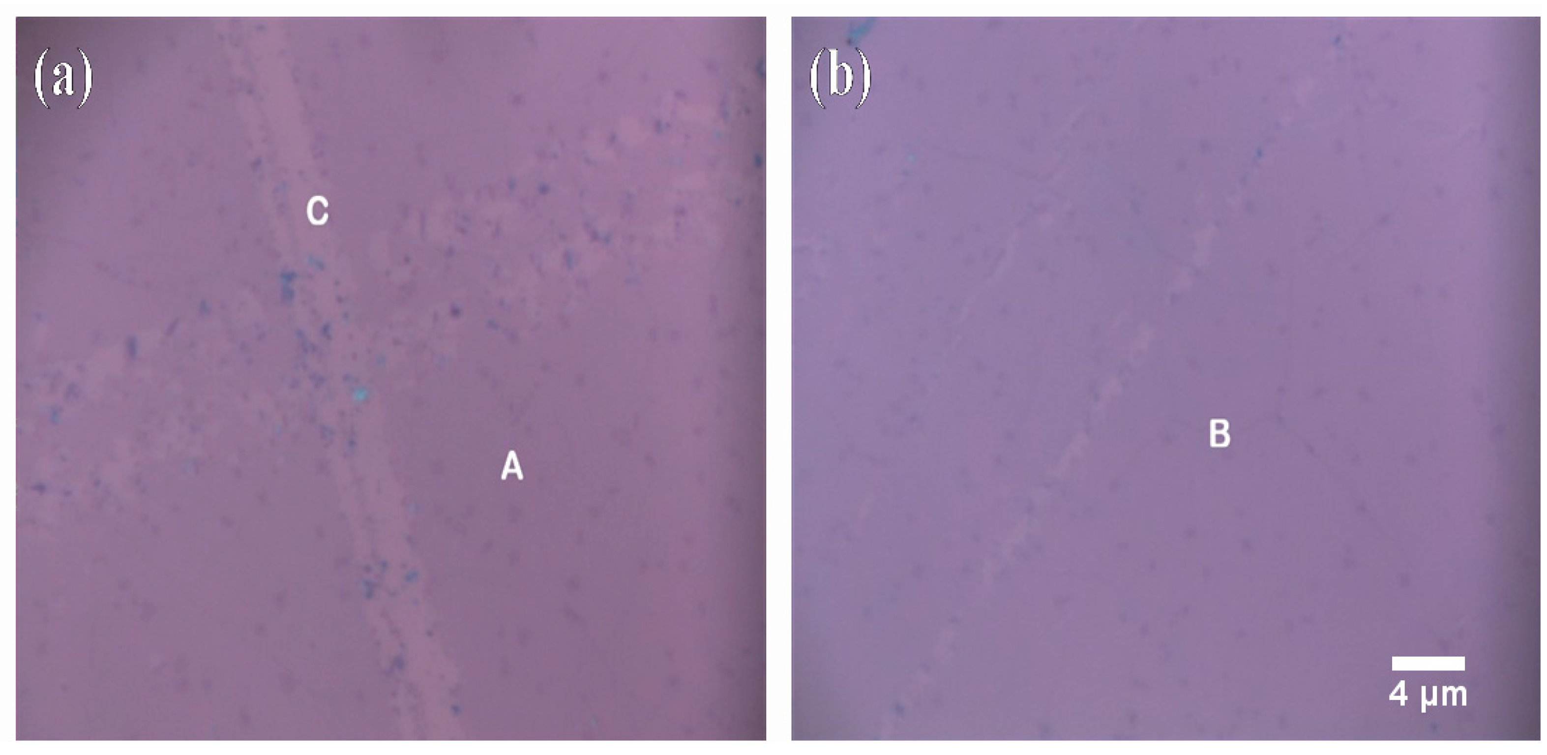
Figure 9.
Illustrative Raman spectra from the central zone (designed as zone A) of the graphene/Si samples. Spectra range from 400 cm−1 to 1100 cm−1 (a) and 1200 cm−1 to 3400 cm−1 (b). This content has been reproduced from Ref. [49] with permission granted by Elsevier. Copyright 2019, Elsevier.
Figure 9.
Illustrative Raman spectra from the central zone (designed as zone A) of the graphene/Si samples. Spectra range from 400 cm−1 to 1100 cm−1 (a) and 1200 cm−1 to 3400 cm−1 (b). This content has been reproduced from Ref. [49] with permission granted by Elsevier. Copyright 2019, Elsevier.
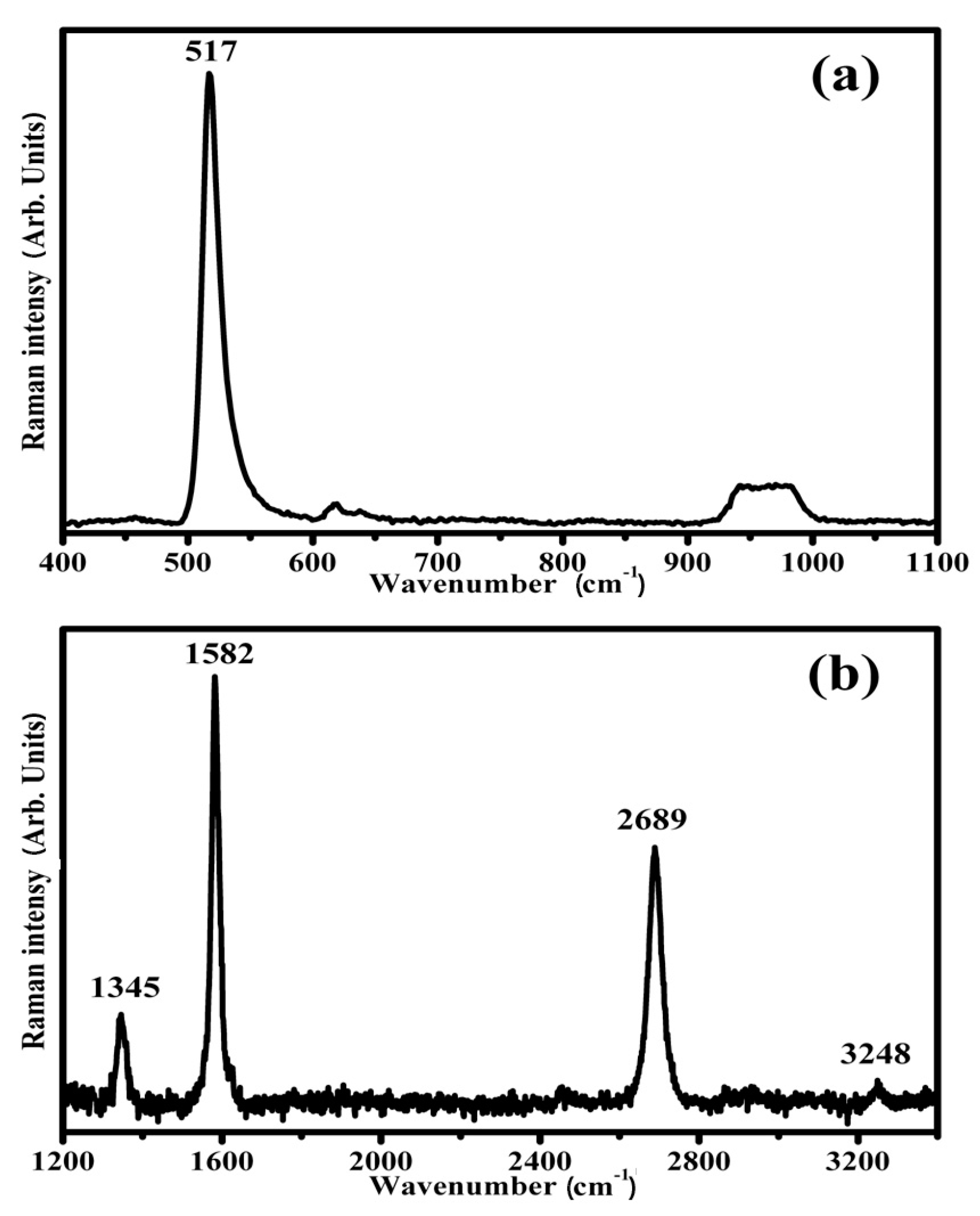
Figure 10.
Illustrative Raman spectra acquired from the border region (zone B) of the graphene/Si samples. Raman spectral profiles spanning the range of 400 cm−1 to 1100 cm−1 (a) and 1200 cm−1 to 3400 cm−1 (b). This content has been reproduced from Ref. [49] with permission granted by Elsevier. Copyright 2019, Elsevier.

Figure 11.
Exemplary Raman spectra obtained from imperfections within the graphene layer (zone C) of the graphene/Si samples. Raman spectral profiles spanning the range of 400 cm−1 to 1100 cm−1 (a) and 1200 cm−1 to 3400 cm−1 (b). This content has been reproduced from Ref. [49] with permission granted by Elsevier. Copyright 2019, Elsevier.

Figure 12.
Representative Raman spectra taken under low laser intensity (OD2 filter) conditions, showcasing graphene oxide thin film dip-coated onto an untreated glass sample (a) and an Ag/graphene oxide/Au sandwich structure (b). This content has been reproduced from Ref. [46] with permission granted by IOP Publishing. Copyright 2019, IOP Publishing.
Disclaimer/Publisher’s Note: The statements, opinions and data contained in all publications are solely those of the individual author(s) and contributor(s) and not of MDPI and/or the editor(s). MDPI and/or the editor(s) disclaim responsibility for any injury to people or property resulting from any ideas, methods, instructions or products referred to in the content. |
© 2023 by the authors. Licensee MDPI, Basel, Switzerland. This article is an open access article distributed under the terms and conditions of the Creative Commons Attribution (CC BY) license (https://creativecommons.org/licenses/by/4.0/).
Share and Cite
MDPI and ACS Style
Politano, G.G.; Versace, C. Recent Advances in the Raman Investigation of Structural and Optical Properties of Graphene and Other Two-Dimensional Materials. Crystals 2023, 13, 1357. https://doi.org/10.3390/cryst13091357
AMA Style
Politano GG, Versace C. Recent Advances in the Raman Investigation of Structural and Optical Properties of Graphene and Other Two-Dimensional Materials. Crystals. 2023; 13(9):1357. https://doi.org/10.3390/cryst13091357
Chicago/Turabian StylePolitano, Grazia Giuseppina, and Carlo Versace. 2023. "Recent Advances in the Raman Investigation of Structural and Optical Properties of Graphene and Other Two-Dimensional Materials" Crystals 13, no. 9: 1357. https://doi.org/10.3390/cryst13091357
Note that from the first issue of 2016, this journal uses article numbers instead of page numbers. See further details here.