1. Introduction
Environmental pollution and the energy crisis have become two of the most severe worldwide problems in the 21st century. Photocatalysis is a very promising technique for both energy and environmental issues due to its direct utilization of solar energy [
1,
2]. In the past four decades, various semiconductors had been developed to be used as photocatalyst, such as TiO
2 [
3], graphite carbon nitride [
4], BiVO
4 [
5], and other newly emerging materials [
6]. However, to date, it is still a great challenge to develop an applicable photocatalyst.
Among various photocatalysts, cadmium sulfide (CdS) is a well-known visible-light-driven material. As a widely-used semiconductor, it has a direct bandgap of around 2.4 eV, which matches well with visible light spectrum, and exhibits excellent photocatalytic activity under sunlight or visible light irradiation [
7,
8]. Thus, it has been applied in a wide range of fields, including optoelectronics, photovoltaics, and photocatalysis [
9]. However, the CdS-based photocatalyst can hardly show its full potential in photocatalysis because of its high recombination rate of photoexcited electron–hole pairs and inherent photocorrosion problem under illumination [
10]. Moreover, the CdS nanoparticles generally aggregate, thus leading to low specific surface area and absorption ability [
11]. Generally, there are three ways to overcome these problems and develop high-efficiency CdS-based photocatalyst. One is the loading of co-catalysts [
12,
13] to enhance the charge separation and transfer. The second is coupling with nanomaterials such as graphene oxide (GO) [
14] and carbon nanotubes (CNTs) [
15] which have large specific surface area in order to increase the active sites. The third strategy is to coat CdS with a thin layer of carbon-based materials (e.g., amorphous carbon [
16] or fullerene [
17]), which is an effective method to enhance the charge separation and protect the surface from photocorrosion. Hydrothermal carbonation carbon (HTCC) is a kind of highly functionalized carbon material [
18] which can couple with metal oxide photocatalysts such as MoO
2 and WO
3 and establish a heterojunction to enhance the charge separation [
19]. However, to the best of our knowledge, there are few reports of HTCC-enhanced CdS.
Herein, we report a facile one-pot hydrothermal preparation (180 °C for 10 h) of HTCC-coated CdS nanocomposite assisted by glucose and polyvinylpyrrolidone (PVP). The PVP is used to decrease the agglomeration of CdS nanoparticles in the reaction system, and the glucose works as the carbon source. The amorphous coating layer of CdS is determined to be HTCC, which mainly contains semiconductive polyfuran. This HTCC-coated CdS shows superior photocatalytic activity and stability for the degradation of RhB under visible light irradiation (λ ≥ 420 nm). This enhancement in activity and stability can mainly be attributed to: (i) The addition of PVP in the reaction solution can significantly increase the specific surface area of CdS, and thus offer more active sites. (ii) The HTCC in the nanocomposite can expand the range of light absorption. (iii) The HTCC layer can form a heterojunction with CdS and improve the charge separation and transfer. This novel CdS-based nanocomposite exhibits great potential in environmental remediation.
2. Results and Discussion
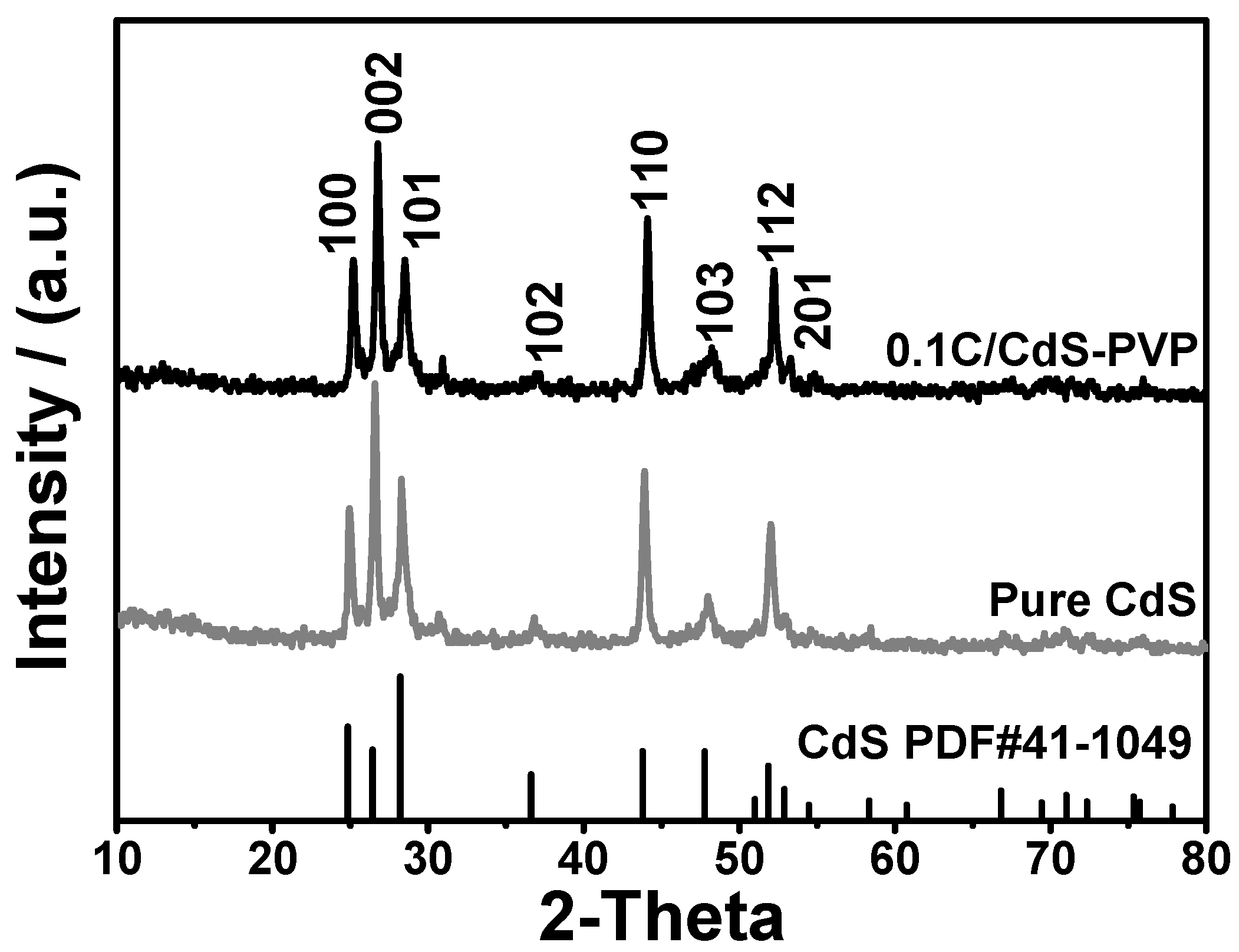
X-ray diffraction (XRD) analysis was used to investigate the crystallographic phase of pure CdS and 0.1C/CdS samples. As shown in
Figure 1, all of the diffraction peaks match well to the hexagonal phase of CdS (JCPDS card No. 41-1049). The peaks at 24.8°, 26.5°, 28.2°, 36.6°, 43.7°, 47.8°, 51.8°, and 52.8° correspond to (100), (002), (101), (102), (110), (103), (112), and (201) planes of hexagonal CdS, respectively. There is no obvious difference of XRD pattern between pure CdS and 0.1C/CdS sample, implying that the crystalline structure of CdS remains unchanged after the introduction of glucose and PVP.
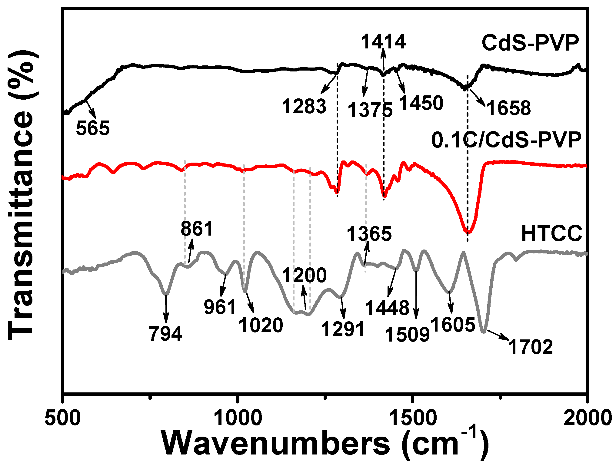
Fourier transform infrared (FT-IR) spectroscopy was conducted to investigate the chemical structure of CdS-PVP, 0.1C/CdS-PVP, and HTCC (
Figure 2). For CdS-PVP and 0.1C/CdS-PVP samples, the weak band around 565 cm
−1 indicates -CS
2 wagging (Cd-S stretching) [
20]. The bands at 1375 and 1450 cm
−1 can be attributed to the Cd-S bonding [
21]. Moreover, both samples contain some characteristic peaks of PVP, such as 1283 cm
−1, 1414 cm
−1, and 1658 cm
−1. For the HTCC, the peaks at 1605 cm
−1, 1448 cm
−1, 1365 cm
−1, and 961 cm
−1 can be assigned to the vibrational modes of the furan monomer [
22]. The band at 1509 cm
−1 is ascribed to the C=C stretching of furan ring in the polymer. Besides, the band at 794 cm
−l is attributed to the linear structure in polyfuran. Moreover, the bands at 1200 cm
−1 and 1020 cm
−1 are ascribed to the C-H bending and stretching modes, and the band at 861 cm
−1 is assigned to the out-of-plane bending of C-H modes [
22]. These bands come from the C-H groups in the furan rings. The band 1702 cm
−1 is ascribed to the C=O stretching, suggesting that some furan rings are open in the polymer, which is common for the polyfuran. Moreover,
13C solid-state CP-MAS NMR spectroscopy was also performed (
Figure S1), and further confirmed the existence of polyfuran in the HTCC [
19]. Therefore, we can infer that the HTCC is mainly composed of polyfuran components, which is in good agreement with previous studies [
18,
19]. Comparing the FT-IR spectra of HTCC and 0.1C/CdS-PVP, we can find some characteristic peaks of HTCC in the 0.1C/CdS-PVP sample, such as 861 cm
−1, 1020 cm
−1, 1200 cm
−1, and 1365 cm
−1. Thus, we can conclude the existence of HTCC in the composite.
The morphology and microstructure are investigated by scanning electron microscopy (SEM) and transmission electron microscopy (TEM) analysis in
Figure 3.
Figure 3a shows the TEM image of an individual pure CdS particle. As shown in
Figure 3b, the 0.1C/CdS-PVP was mostly composed of nanocrystals with polygonal morphology with the size of c.a. 60 nm, and others were irregular particles.
Figure 3c displays a TEM image of a 0.1C/CdS-PVP particle. In
Figure 3c, a homogeneous amorphous layer coating on the surface of CdS nanocrystals with intimate contact can be clearly observed. This TEM image demonstrates that the 0.1C/CdS-PVP consisted of core–shell structures. Combining the results of XRD and FT-IR, we can infer that the amorphous layer is HTCC components in the 0.1C/CdS-PVP sample.
Figure 3d displays a high-resolution TEM (HRTEM) image of 0.1C/CdS-PVP sample. The lattice fringes are measured to be 0.316 nm, which agree well with the (111) plane of hexagonal CdS. Through HRTEM observation, it can be measured that the thickness of the HTCC layer was as thin as 4–6 nm, which will not block the visible light illumination to the CdS. As expected, the layer was observed in other CdS/C-PVP nanocomposites (
Figure S2). The thickness of the HTCC layer varied from 2 to 10 nm with the addition of glucose (0.05–0.5 g). The formation of the carbon shell may be formed by the adsorption of fractional amorphous carbon generated from the hydrothermal carbonization process. In addition, the thermal gravimetric analysis (TGA) curves of CdS-PVP and 0.1C/CdS-PVP samples are recorded from room temperature to 550 °C in air with a heating rate of 10 °C·min
−1 (
Figure S3). The two samples display a decrease in weight loss from 300–500 °C, which can be attributed to the decomposition of PVP, the oxidation of CdS, and the removal of HTCC. Thus, we infer that the difference between CdS-PVP and 0.1C/CdS-PVP samples is the amount of HTCC in 0.1C/CdS-PVP, which is approximately 1.96 wt %.
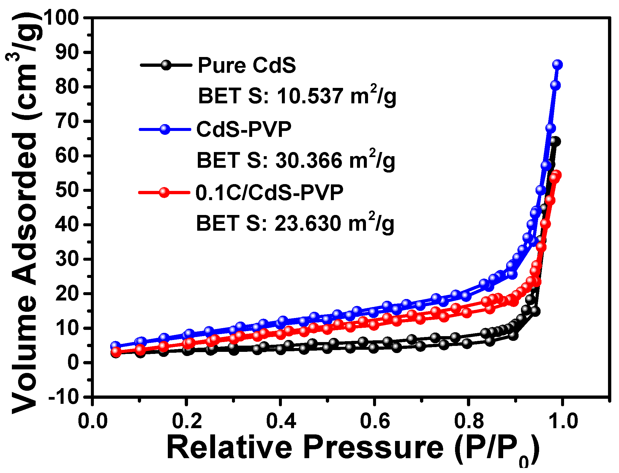
Figure 4 shows the nitrogen adsorption–desorption isotherms and corresponding Brunauer–Emmett–Teller (BET) surface area of the pure CdS, CdS-PVP, and 0.1C/CdS-PVP samples. As shown in
Figure 4, the BET surface areas of the three samples were as follows: 10.537 m
2/g for pure CdS, 30.366 m
2/g for CdS-PVP, and 23.630 m
2/g for 0.1C/CdS-PVP. The corresponding pore size distributions of the three samples ranged from about 2 nm to 50 nm and centered at ca. 20 nm (
Figure S4). It should be noted that the surface area of CdS-PVP was two times higher than that of pure CdS, even with the addition of a small amount of PVP (0.3 g). This is because PVP is a widely-used water dispersible and structure-directing reagent [
23,
24], which is beneficial to avoiding the agglomeration of CdS particles. A photocatalyst with larger specific surface is beneficial for its photocatalytic activity because of enhanced absorption ability. Compared to CdS-PVP, the BET surface area of 0.1C/CdS-PVP sample decreases slightly. This phenomenon is caused by the coating carbon layer, which may work as adhesive to connect the dispersive CdS particles.
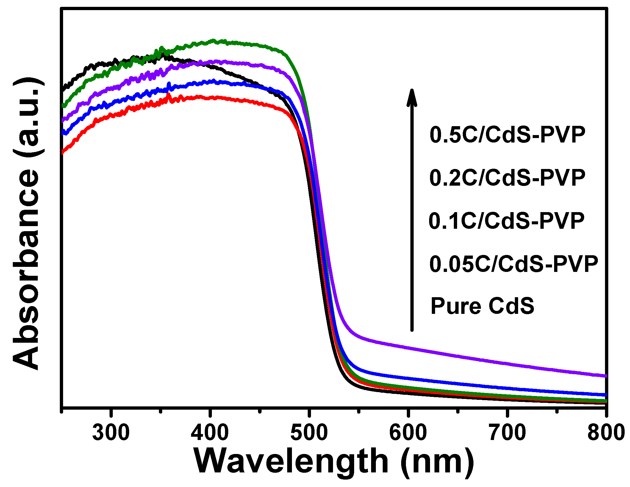
A comparison of the UV-vis diffuse reflectance spectra of pure CdS, 0.05CdS-PVP, 0.1CdS-PVP, 0.2CdS-PVP, and 0.5CdS-PVP samples is displayed in
Figure 5. All of the samples exhibit a similar absorption edge at around 520 nm, which corresponds to the intrinsic band gap of CdS. Compared to pure CdS, the absorbance of visible light over all C/CdS-PVP samples was enhanced. Additionally, the color of CdS-PVP samples became darker with the increasing glucose contents. It is well-known that a darker photocatalyst will lead to an enhanced light absorption ability, thus improving its photocatalytic activity. In addition, the band gap of the samples is further determined by the linear approximation in the Kubelka–Munk plots (
Figure S5). The results show that the band gaps of the C/CdS-PVP samples are similar.
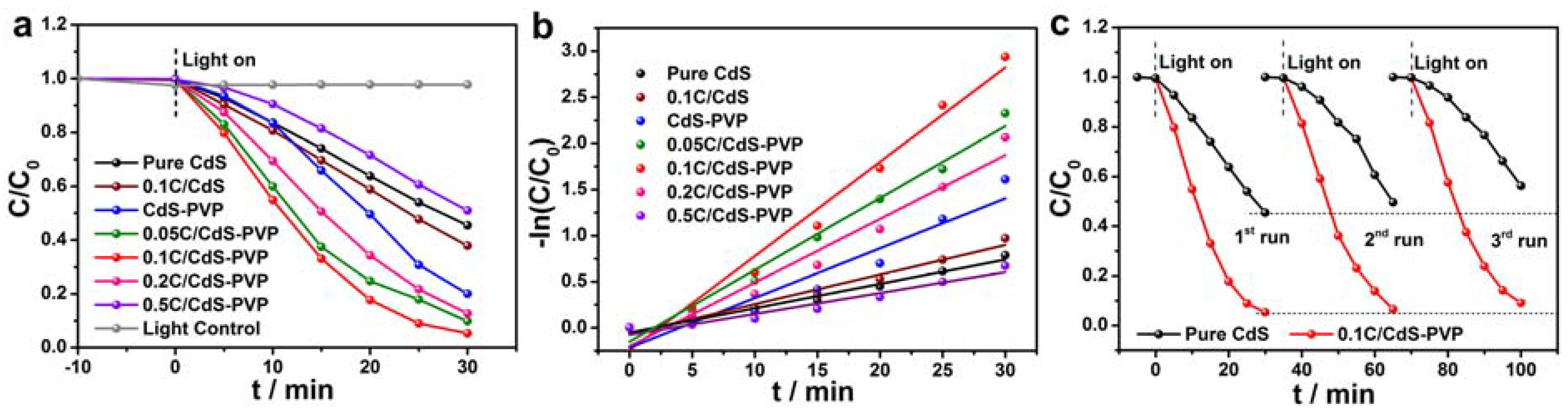
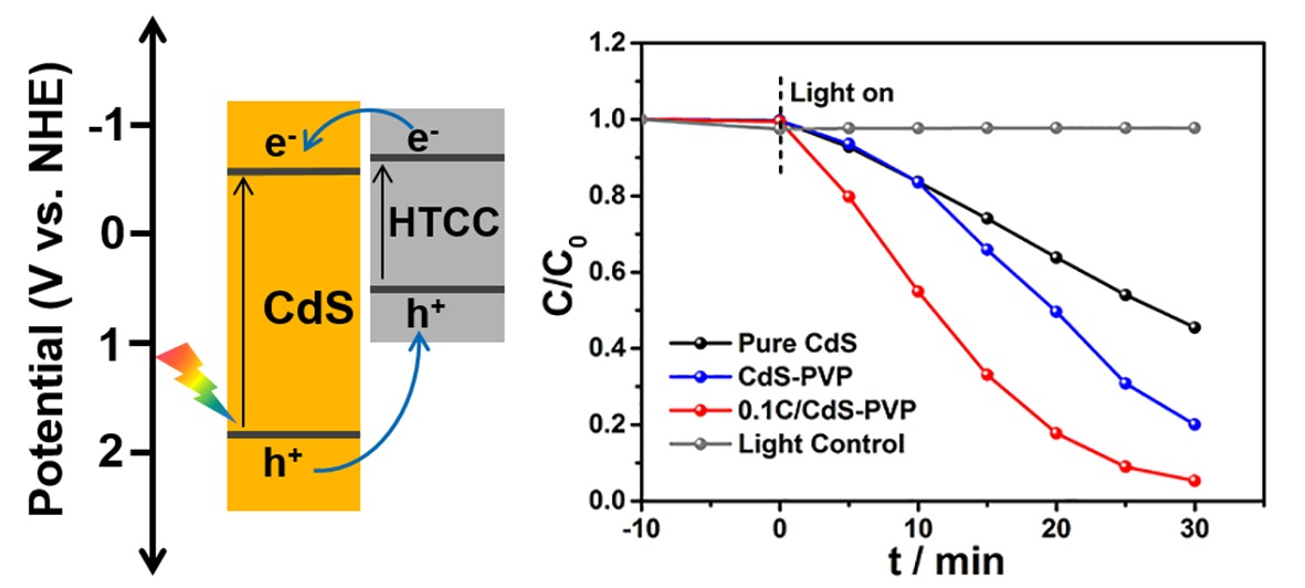
To evaluate the photocatalytic performance of the as-prepared samples, photocatalytic degradation of RhB was conducted under visible light irradiation.
Figure 6a presents the degradation efficiencies of C/CdS-PVP with different contents of glucose, pure CdS, and CdS-PVP samples. As presented in
Figure 6a, pure CdS exhibits a limited degradation efficiency of 54.5% in 30 min due to the rapid recombination of charge carriers. However, the degradation efficiency of CdS-PVP increases to 80.0% with the introduction of PVP additive. Such a large increase benefits by the improved specific surface area and absorption ability of CdS-PVP. Additionally, the larger specific surface area of CdS-PVP has more active sites and reaction centers for photocatalytic reaction, which facilitate an enhanced activity. The degradation efficiency of C/CdS-PVP further increases after the carbon coating on the CdS. After irradiation for 30 min, the degradation efficiencies over different C/CdS-PVP are 90.2% (0.05C/CdS-PVP), 94.7% (0.1C/CdS-PVP), 87.3% (0.2C/CdS-PVP), and 49.0% (0.5C/CdS-PVP). Therefore, we confirm that the optimum amount of glucose was 0.1 g.
It can be observed that the 0.5C/CdS-PVP sample showed a very low activity, even lower than that of the pure CdS. This is attributed to two factors: (1) A greater content of glucose in the precursor will lead to thicker HTCC layer and decrease the light intensity on the surface of CdS. (2) The reaction rate of the carbonization of the glucose will become faster, resulting in the formation of carbon nanospheres with larger size when the concentration of glucose is raised (
Figure S6). Thus, the large amounts of black carbon nanospheres would shield the visible light, which is called a “shielding effect” [
14], resulting in a rapid decrease of activity. Therefore, a suitable content of glucose is crucial for the optimal activity. It should be pointed out that the 0.1C/CdS sample also exhibits a low photocatalytic activity, similar to the pure CdS. This may be attributed to the serious agglomeration of CdS particles. In this case, there is only a small quantity of amorphous carbon that can adsorb on the surface of CdS, and most tend to form carbon colloid spheres. Additionally, the corresponding reaction kinetics of the degradation are calculated and shown in
Figure 6b. The 0.1C/CdS-PVP sample showed the highest apparent reaction rate, which is nearly four times as high as that of pure CdS (0.102 min
–1 vs. 0.026 min
–1). Moreover, the 0.1C/CdS-PVP sample showed a superior stability compared to pure CdS. As shown in
Figure 6c, there was only a 3.8% decrease of degradation efficiency for 0.1C/CdS-PVP sample after three recycling degradation, while pure CdS had a 10.9% decrease.
On the basis of the above results and discussion, we can infer that the PVP and the thin layer of HTCC have a significant effect on the process of photocatalytic degradation. Firstly, the addition of PVP in the reaction solution can significantly increase the specific surface area of CdS and offer more active adsorption sites and reaction centers. Secondly, the thin layer of HTCC can improve the adsorption ability of light. Finally, the separation of charge carriers in the CdS can be effectively improved.
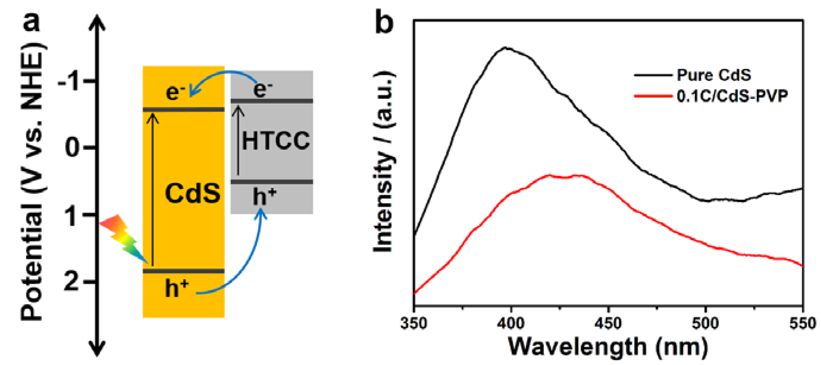
Recently, our group found that the HTCC derived from glucose is a polyfuran-based
n-type semiconductor, containing plenty of sp
2-hybridization structures [
19,
25]. Under solar light illumination, HTCC generates photoexcited electrons, holes, and hydroxyl radicals. These species can be used for photocatalytic treatment such as water disinfection and the degradation of organic pollutants. Combining the FT-IR,
13C NMR, XRD, and TEM, we can infer that the coverage layer on the surface of CdS is also HTCC mainly containing the polyfuran, like those in our previous report. Therefore, according to the above literatures, the conduction band (CB) and valence band (VB) position of HTCC are estimated to be about −0.65 V (
vs. NHE, Normal Hydrogen Electrode) and +0.54 V (
vs. NHE). Therefore, a proper p-n heterojunction is constructed base on the intimate contact between the CdS (the CB is −0.97 V
vs. NHE and VB is +1.48 V
vs. NHE) and HTCC (
Figure 7a). Under illumination, the valence electrons (e
−) in the CdS can be excited to the conduction band (CB) and leaving holes (h
+) in the valence band (VB). Then, the holes in the CdS will transfer to the HTCC with higher valance band maximum and survive from being recombined. They can then migrate to the solution through the conductive polyfuran domains and participate in photocatalytic reactions. Therefore, only a fraction of holes can photocorrode the CdS nanocrystals, and achieve an enhanced photocatalytic activity and stability. On the other hand, the HTCC can also generate photoexcited electrons and transfer to the CB of CdS, which is beneficial to the separation of photoinduced charge carriers. Moreover, the photoluminescence (PL) emission spectra were recorded to investigate the charge recombination process in pure CdS and 0.1C/CdS-PVP samples. As shown in
Figure 7b, the pure CdS exhibited stronger PL intensity 0.1C/CdS-PVP, suggesting the higher charge recombination process in the pure CdS. Consequently, a better photocatalytic performance of 0.1C/CdS-PVP is expected.


