Reliability of NAND Flash Memories: Planar Cells and Emerging Issues in 3D Devices


Abstract
:1. Introduction
2. The NAND Memory Array
2.1. Array Architecture and Layout
2.2. Array Operation
2.2.1. Read
2.2.2. Program
2.2.3. Erase
3. NAND Flash Memory Reliability
3.1. Endurance
3.2. Random Telegraph Noise (RTN)
3.2.1. RTN Amplitude
3.2.2. Main Experimental Data
3.2.3. Models
3.2.4. Effect on Programmed Distribution
3.3. Retention after Cycling and SILC
3.4. Charge Detrapping
3.4.1. Main Experimental Data
3.4.2. Models
3.4.3. Effect on Distribution after Cycling
3.5. Interface State Recovery
3.6. Disturbs
3.6.1. Read Disturb
3.6.2. Program and Pass Disturbs
4. 3D NAND Reliability
4.1. Endurance
4.2. Retention
4.3. Cell Current Fluctuations
4.3.1. Random Telegraph Noise
4.3.2. Polysilicon Grains
4.4. Disturbs
5. Conclusions
Acknowledgments
Conflicts of Interest
References
- Harari, E. Electrically Erasable Non-Volatile Semiconductor Memory. U.S. Patent 4,115,914, 26 September 1978. [Google Scholar]
- Masuoka, F.; Asano, M.; Iwahashi, H.; Komuro, T.; Tanaka, S. A new Flash E2PROM cell using triple polysilicon technology. In Proceedings of the 1984 International Electron Devices Meeting, San Francisco, CA, USA, 9–12 December 1984; pp. 464–467. [Google Scholar]
- Masuoka, F.; Momodomi, M.; Iwata, Y.; Shirota, R. New ultra high density EPROM and Flash EEPROM with NAND structure cell. In Proceedings of the 1987 International Electron Devices Meeting, New York, NY, USA, 6–9 December 1987; pp. 552–555. [Google Scholar]
- Micheloni, R.; Marelli, A.; Eshghi, K. (Eds.) Inside Solid State Drives (SSDs); Springer: Heidelberg/Berlin, Germany, 2013. [Google Scholar]
- Fontana, R.E.; Decad, G.M.; Hetzler, S.R. Volumetric density trends (TB/in.3) for storage components: Tape, hard disk drives, NAND, and blu-ray. J. Appl. Phys. 2015, 117, 17E301-1–17E301-4. [Google Scholar] [CrossRef]
- Tokutomi, T.; Doi, M.; Hachiya, S.; Kobayashi, A.; Tanakamaru, S.; Takeuchi, K. Enterprise-grade 6x fast read and 5x highly reliable SSD with TLC NAND-Flash memory for Big-Data storage. In Proceedings of the 2015 IEEE International Solid-State Circuits Conference (ISSCC), San Francisco, CA, USA, 22–26 February 2015; pp. 140–142. [Google Scholar]
- Kim, H.J.; Lim, J.D.; Lee, J.W.; Na, D.H.; Shin, J.H.; Kim, C.H.; Yu, S.W.; Shin, J.Y.; Lee, S.K.; Rajagopal, D.; et al. 1 GB/s 2 Tb NAND Flash multi-chip package with frequency-boosting interface chip. In Proceedings of the 2015 IEEE International Solid-State Circuits Conference (ISSCC), San Francisco, CA, USA, 22–26 February 2015; pp. 138–140. [Google Scholar]
- Choi, S.; Kim, D.; Choi, S.; Kim, B.; Jung, S.; Chun, K.; Kim, N.; Lee, W.; Shin, T.; Jin, H.; et al. A 93.4 mm2 64 Gb MLC NAND-Flash memory with 16 nm CMOS technology. In Proceedings of the 2014 IEEE International Solid-State Circuits Conference (ISSCC), San Francisco, CA, USA, 9–13 February 2014; pp. 328–329. [Google Scholar]
- Helm, M.; Park, J.K.; Ghalam, A.; Guo, J.; wan Ha, C.; Hu, C.; Kim, H.; Kavalipurapu, K.; Lee, E.; Mohammadzadeh, A.; et al. A 128 Gb MLC NAND-Flash device using 16 nm planar cell. In Proceedings of the 2014 IEEE International Solid-State Circuits Conference (ISSCC), San Francisco, CA, USA, 9–13 February 2014; pp. 326–327. [Google Scholar]
- Lee, S.; Lee, J.-Y.; Park, I.-H.; Park, J.; Yun, S.-W.; Kim, M.-S.; Lee, J.-H.; Kim, M.; Lee, K.; Kim, T.; et al. A 128 Gb 2b/cell NAND Flash memory in 14nm technology with tPROG = 640 μs and 800 MB/s I/O rate. In Proceedings of the 2014 IEEE International Solid-State Circuits Conference (ISSCC), San Francisco, CA, USA, 31 January–4 February 2016; pp. 138–139. [Google Scholar]
- Sako, M.; Watanabe, Y.; Nakajima, T.; Sato, J.; Muraoka, K.; Fujiu, M.; Kouno, F.; Nakagawa, M.; Masuda, M.; Kato, K.; et al. A low-power 64 Gb MLC NAND-Flash memory in 15 nm CMOS technology. In Proceedings of the 2015 IEEE International Solid-State Circuits Conference (ISSCC), San Francisco, CA, USA, 22–26 February 2015; pp. 128–129. [Google Scholar]
- Prall, K.; Parat, K. 25 nm 64 Gb MLC NAND technology and scaling challenges. In Proceedings of the 2010 IEEE International Electron Devices Meeting (IEDM), San Francisco, CA, USA, 6–8 December 2010; pp. 102–105. [Google Scholar]
- Goda, A.; Parat, K. Scaling directions for 2D and 3D NAND cells. In Proceedings of the 2012 IEEE International Electron Devices Meeting (IEDM), San Francisco, CA, USA, 10–13 December 2012; pp. 2.1.1–2.1.4. [Google Scholar]
- Lee, S. Scaling challenges in NAND Flash device toward 10 nm technology. In Proceedings of the 2012 4th IEEE International Memory Workshop (IMW), Milan, Italy, 20–23 May 2012; pp. 1–4. [Google Scholar]
- Monzio Compagnoni, C.; Goda, A.; Spinelli, A.S.; Feeley, P.; Lacaita, A.L.; Visconti, A. Reviewing the evolution of the NAND Flash technology. Proc. IEEE 2017. [Google Scholar] [CrossRef]
- Endoh, T.; Kinoshita, K.; Tanigami, T.; Wada, Y.; Sato, K.; Yamada, K.; Yokoyama, T.; Takeuchi, N.; Tanaka, K.; Awaya, N.; et al. Novel ultra high density Flash memory with a stacked-surrounding gate transistor (S-SGT) structured cell. In Proceedings of the 2001 International Electron Devices Meeting (IEDM’01), Washington, DC, USA, 2–5 December 2001; pp. 33–36. [Google Scholar]
- Jung, S.M.; Jang, J.; Cho, W.; Cho, H.; Jeong, J.; Chang, Y.; Kim, J.; Rah, Y.; Son, Y.; Park, J.; et al. Three dimensionally stacked NAND Flash memory technology using stacking single crystal Si layers on ILD and TANOS structure for beyond 30 nm node. In Proceedings of the 2006 International Electron Devices Meeting (IEDM), San Francisco, CA, USA, 11–13 December 2006; pp. 37–40. [Google Scholar]
- Lai, E.K.; Lue, H.T.; Hsiao, Y.H.; Hsieh, J.Y.; Lu, C.P.; Wang, S.Y.; Yang, L.W.; Yang, T.; Chen, K.C.; Gong, J.; et al. A multi-layer stackable thin-film transistor (TFT) NAND-type Flash memory. In Proceedings of the 2006 International Electron Devices Meeting (IEDM), San Francisco, CA, USA, 11–13 December 2006; pp. 41–44. [Google Scholar]
- Park, K.T.; Kim, D.; Hwang, S.; Kang, M.; Cho, H.; Jeong, Y.; Seo, Y.I.; Jang, J.; Kim, H.S.; Jung, S.M.; et al. A 45 nm 4Gb 3-dimensional double-stacked multi-Level NAND Flash memory with shared bitline structure. In Proceedings of the 2008 IEEE International Solid-State Circuits Conference—Digest of Technical Papers, San Francisco, CA, USA, 3–7 February 2008; pp. 510–511. [Google Scholar]
- Tanaka, H.; Kido, M.; Yahashi, K.; Oomura, M.; Katsumata, R.; Kito, M.; Fukuzumi, Y.; Sato, M.; Nagata, Y.; Matsuoka, Y.; et al. Bit cost scalable technology with punch and plug process for ultra high density Flash memory. In Proceedings of the 2007 IEEE Symposium on VLSI Technology, Kyoto, Japan, 12–14 June 2007; pp. 14–15. [Google Scholar]
- Park, K.T.; Han, J.M.; Kim, D.; Nam, S.; Choi, K.; Kim, M.-S.; Kwak, P.; Lee, D.; Choi, Y.H.; Kang, K.M.; et al. Three-dimensional 128Gb MLC vertical NAND Flash-memory with 24-WL stacked layers and 50MB/s high-speed programming. In Proceedings of the 2014 IEEE International Solid-State Circuits Conference (ISSCC), San Francisco, CA, USA, 9–13 February 2014; pp. 334–335. [Google Scholar]
- Park, K.T.; Nam, S.; Kim, D.; Kwak, P.; Lee, D.; Choi, Y.H.; Choi, M.H.; Kwak, D.H.; Kim, D.H.; Kim, M.S.; et al. Three-dimensional 128 Gb MLC vertical NAND Flash memory with 24-WL stacked layers and 50 MB/s high-speed programming. IEEE J. Solid-State Circuits 2015, 50, 204–213. [Google Scholar] [CrossRef]
- Tanaka, T.; Helm, M.; Vali, T.; Ghodsi, R.; Kawai, K.; Park, J.K.; Yamada, S.; Pan, F.; Einaga, Y.; Ghalam, A.; et al. A 768Gb 3b/cell 3D-floating-gate NAND Flash memory. In Proceedings of the 2014 IEEE International Solid-State Circuits Conference (ISSCC), San Francisco, CA, USA, 31 January–4 February 2016; pp. 142–143. [Google Scholar]
- Yamashita, R.; Magia, S.; Higuchi, T.; Yoneya, K.; Yamamura, T.; Mizukoshi, H.; Zaitsu, S.; Yamashita, M.; Toyama, S.; Kamae, N.; et al. A 512Gb 3b/cell Flash memory on 64-word-line-layer BiCS technology. In Proceedings of the 2017 IEEE International Solid- State Circuits Conference (ISSCC), San Francisco, CA, USA, 5–9 February 2017; pp. 196–198. [Google Scholar]
- Kim, C.; Cho, J.H.; Jeong, W.; Park, I.H.; Park, H.W.; Kim, D.H.; Kang, D.; Lee, S.; Lee, J.S.; Kim, W.; et al. A 512 Gb 3b/cell 64-stacked WL 3D V-NAND Flash memory. In Proceedings of the 2017 IEEE International Solid- State Circuits Conference (ISSCC), San Francisco, CA, USA, 5–9 February 2017; pp. 202–204. [Google Scholar]
- Shirota, R. Developments in 3D-NAND Flash technology. In Advances in Non-Volatile Memory and Storage Technology; Nishi, Y., Ed.; Elsevier: Amsterdam, The Netherlands, 2014; Chapter 2; pp. 27–74. [Google Scholar]
- Aritome, S. NAND Flash Memory Technologies; John Wiley & Sons: Hoboken, NJ, USA, 2015. [Google Scholar]
- Micheloni, R. (Ed.) 3D Flash Memories; Springer: Heidelberg/Berlin, Germany, 2016. [Google Scholar]
- Lee, J.; Jang, J.; Lim, J.; Shin, Y.G.; Lee, K.; Jung, E. A new ruler on the market: 3D-NAND flash for high-density memory and its technology evolution and challenges on the future. In Proceedings of the 2016 International Electron Devices Meeting (IEDM), San Francisco, CA, USA, 3–7 December 2016; pp. 11.2.1–11.2.4. [Google Scholar]
- Nonvolatile Memory Technology with Emphasis on Flash; Brewer, J.E.; Gill, M. (Eds.) Wiley-IEEE Press: Hoboken, NJ, USA, 2008. [Google Scholar]
- Inside NAND Flash Memories; Micheloni, R.; Crippa, L.; Marelli, A. (Eds.) Springer: Heidelberg/Berlin, Germany, 2010. [Google Scholar]
- Pavan, P.; Bez, R.; Olivo, P.; Zanoni, E. Flash memory cells—An overview. Proc. IEEE 1997, 85, 1248–1271. [Google Scholar] [CrossRef]
- Aritome, S.; Satoh, S.; Maruyama, T.; Watanabe, H.; Shuto, S.; Hemink, G.J.; Shirota, R.; Watanabe, S.; Masuoka, F. A 0.67 μm2 self-aligned shallow trench isolation cell (SA-STI cell) for 3 V-only 256 Mbit NAND EEPROMs. In Proceedings of the 1994 International Electron Devices Meeting (IEDM), San Francisco, CA, USA, 11–14 December 1994; pp. 61–64. [Google Scholar]
- Naso, G.; Botticchio, L.; Castelli, M.; Cerafogli, C.; Cichocki, M.; Conenna, P.; D’Alessandro, A.; Santis, L.D.; Di Cicco, D.; Di Francesco, W.; et al. A 128 Gb 3 b/cell NAND Flash design using 20 nm planar-cell technology. In Proceedings of the 2013 IEEE International Solid-State Circuits Conference (ISSCC), San Francisco, CA, USA, 17–21 February 2013; pp. 218–219. [Google Scholar]
- Bauer, M.; Alexis, R.; Atwood, G.; Baltar, B.; Fazio, A.; Frary, K.; Hensel, M.; Ishac, M.; Javanifard, J.; Landgraf, M.; et al. A Multilevel-cell 32 Mb Flash memory. In Proceedings of the 1995 IEEE International Solid-State Circuits Conference, San Francisco, CA, USA, 15–17 February 1995; pp. 132–133. [Google Scholar]
- Jung, T.S.; Choi, Y.J.; Suh, K.D.; Suh, B.H.; Kim, J.K.; Lim, Y.H.; Koh, Y.N.; Park, J.W.; Lee, K.J.; Park, J.H.; et al. A 117-mm23.3-V only 128-Mb multilevel NAND Flash memory for mass storage applications. IEEE J. Solid-State Circuits 1996, 31, 1575–1583. [Google Scholar] [CrossRef]
- Shibata, N.; Maejima, H.; Isobe, K.; Iwasa, K.; Nakagawa, M.; Fujiu, M.; Shimizu, T.; Honma, M.; Hoshi, S.; Kawaai, T.; et al. A 70 nm 16 Gb 16-level-cell NAND flash memory. IEEE J. Solid-State Circuits 2008, 43, 929–937. [Google Scholar] [CrossRef]
- Micheloni, R.; Crippa, L. Multi-bit NAND Flash memories for ultra-high density storage devices. In Advances in Non-Volatile Memory and Storage Technology; Nishi, Y., Ed.; Woodhead Publishing: Amsterdam, The Netherlands, 2014; Chapter 3; pp. 75–119. [Google Scholar]
- Aritome, S.; Shirota, R.; Kirisawa, R.; Endoh, T.; Nakayama, R.; Sakui, K.; Masuoka, F. A reliable bi-polarity write/erase technology in Flash EEPROMs. In Proceedings of the 1990 International Electron Devices Meeting (IEDM), San Francisco, CA, USA, 9–12 December 1990; pp. 111–114. [Google Scholar]
- Hemink, G.J.; Tanaka, T.; Endoh, T.; Aritome, S.; Shirota, R. Fast and accurate programming method for multi-level NAND EEPROMs. In Proceedings of the 1995 Symposium on VLSI Technology—Digest of Technical Papers, Kyoto, Japan, 6–8 June 1995; pp. 129–130. [Google Scholar]
- Micheloni, R.; Marelli, A.; Ravasio, R. Error-Correction Codes for Non-Volatile Memories; Springer: Heidelberg/Berlin, Germany, 2008. [Google Scholar]
- Zhao, K.; Zhao, W.; Sun, H.; Zhang, T.; Zhang, X.; Zheng, N. LDPC-in-SSD: Making advanced error correction codes work effectively in solid state drives. In Proceedings of the 11th USENIX Conference on File and Storage Technologies, San Jose, CA, USA, 12–15 February 2013; pp. 243–256. [Google Scholar]
- Wang, J.; Vakilinia, K.; Chen, T.Y.; Courtade, T.; Dong, G.; Zhang, T.; Shankar, H.; Wesel, R. Enhanced precision through multiple reads for LDPC decoding in Flash memories. IEEE J. Sel. Areas Commun. 2014, 32, 880–891. [Google Scholar] [CrossRef]
- Lin, W.; Yen, S.W.; Hsu, Y.C.; Lin, Y.H.; Liang, L.C.; Wang, T.C.; Shih, P.Y.; Lai, K.H.; Cheng, K.Y.; Chang, C.Y. A low power and ultra high reliability LDPC error correction engine with digital signal processing for embedded NAND Flash controller in 40nm CMOS. In Proceedings of the 2014 Symposium on VLSI Technology (VLSI-Technology): Digest of Technical Papers, Honolulu, HI, USA, 9–12 June 2014; pp. 101–102. [Google Scholar]
- Haymaker, K.; Kelley, C.A. Structured bit-interleaved LDPC codes for MLC Flash memory. IEEE J. Sel. Areas Commun. 2014, 32, 870–879. [Google Scholar] [CrossRef]
- Cho, S.-G.; Kim, D.; Choi, J.; Ha, J. Block-wise concatenated BCH codes for NAND Flash memories. IEEE Trans. Commun. 2014, 62, 1164–1177. [Google Scholar] [CrossRef]
- Kim, D.; Ha, J. Quasi-primitive block-wise concatenated BCH codes for NAND Flash memories. In Proceedings of the 2014 IEEE Information Theory Workshop (ITW), Hobart, Australia, 2–5 November 2014; pp. 611–615. [Google Scholar]
- Spinner, J.; Rajab, M.; Freudenberger, J. Construction of high-rate generalized concatenated codes for applications in non-volatile Flash memories. In Proceedings of the 2016 IEEE Information Theory Workshop (ITW), Cambridge, UK, 11–14 September 2016. [Google Scholar]
- Spinner, J.; Freudenberger, J.; Shavgulidze, S. A soft input decoding algorithm for generalized concatenated codes. IEEE Trans. Commun. 2016, 64, 3585–3595. [Google Scholar] [CrossRef]
- Garvin, P.K.; Stanard, H.D. Method and System for Managing Bad Areas in Flash Memories. U.S. Patent 6,260,156 B1, 10 July 2001. [Google Scholar]
- Verma, G.; Mielke, N. Reliability performance of ETOX based Flash memories. In Proceedings of the 26th Annual Proceedings, International Reliability Physics Symposium, Monterey, CA, USA, 12–14 April 1988; pp. 158–166. [Google Scholar]
- Aritome, S.; Shirota, R.; Hemink, G.; Endoh, T.; Masuoka, F. Reliability issues of Flash memory cells. Proc. IEEE 1993, 81, 776–788. [Google Scholar] [CrossRef]
- Cappelletti, P.; Modelli, A. Flash memory reliability. In Flash Memories; Cappelletti, P., Golla, C., Olivo, P., Zanoni, E., Eds.; Kluwer: Dordrecht, The Netherlands, 1999. [Google Scholar]
- Tao, G.; Valk, H.; Scarpa, A.; van Marwijk, L.; Kuper, F.G.; Dormans, G.J.M.; Verhaar, R.D.J. Reliability aspects of advanced embedded floating-gate non-volatile memories with uniform channel FN tunneling for both program and erase. In Proceedings of the Non-Volatile Semiconductor Memory Workshop, Monterey, CA, USA, 12–15 August 2001; pp. 130–132. [Google Scholar]
- Cappelletti, P.; Bez, R.; Modelli, A.; Visconti, A. What we have learned on Flash memory reliability in the last ten years. In Proceedings of the 2004 International Electron Devices Meeting (IEDM), San Francisco, CA, USA, 13–15 December 2004; pp. 489–492. [Google Scholar]
- Ielmini, D.; Spinelli, A.S.; Lacaita, A.L. Recent developments on Flash memory reliability. Microelectron. Eng. 2005, 80C, 321–328. [Google Scholar] [CrossRef]
- Monzio Compagnoni, C.; Spinelli, A.S.; Lacaita, A.L.; Ghetti, A.; Visconti, A. Emerging constraints on NAND Flash memory reliability. In Nonvolatile Memories: Materials, Devices and Applications; American Scientific Publishers: Valencia, CA, USA, 2012; pp. 267–293. [Google Scholar]
- Zambelli, C.; Olivo, P. SSD reliability. In Inside Solid-State Drives (SSD)s; Micheloni, R., Marelli, A., Eshghi, K., Eds.; Springer: Heidelberg/Berlin, Germany, 2013; Chapter 8; pp. 203–231. [Google Scholar]
- Park, Y.; Lee, J.; Cho, S.S.; Jin, G.; Jung, E. Scaling and reliability of NAND Flash devices. In Proceedings of the 2014 IEEE International Reliability Physics Symposium (IRPS), Waikoloa, HI, USA, 1–5 June 2014; pp. 2E.1.1–2E.1.4. [Google Scholar]
- Mielke, N.; Marquart, T.; Wu, N.; Kessenich, J.; Belgal, H.; Schares, E.; Trivedi, F.; Goodness, E.; Nevill, L.R. Bit error rate in NAND Flash memories. In Proceedings of the IEEE International Reliability Physics Symposium, Phoenix, AZ, USA, 27 April–1 May 1 2008; pp. 9–19. [Google Scholar]
- Meza, J.; Wu, Q.; Kumar, S.; Mutlu, O. A large-scale study of Flash memory failures in the field. In Proceedings of the ACM SIGMETRICS—International Conference on Measurement and Modeling of Computer Systems, Portland, OR, USA, 15–19 June 2015; pp. 177–190. [Google Scholar]
- Schroeder, B.; Lagisetty, R.; Merchant, A. Flash reliability in production: the expected and the unexpected. In Proceedings of the 14th USENIX Conference on File and Storage Technologies (FAST’16), Santa Clara, CA, USA, 22–25 February 2016; pp. 67–80. [Google Scholar]
- Lee, J.D.; Choi, J.H.; Park, D.; Kim, K. Effects of interface trap generation and annihilation on the data retention characteristics of Flash memory cells. IEEE Trans. Device Mater. Reliab. 2004, 4, 110–117. [Google Scholar] [CrossRef]
- Itsumi, M. Positive and negative charging of thermally-grown SiO2 induced by Fowler-Nordheim emission. J. Appl. Phys. 1981, 52, 3491–3497. [Google Scholar] [CrossRef]
- Maserjian, J.; Zamani, N. Behavior of the Si/SiO2 interface observed by Fowler-Nordheim tunneling. J. Appl. Phys. 1982, 53, 559–567. [Google Scholar] [CrossRef]
- Maserjian, J.; Zamani, N. Observation of positively charged state generation near the Si/SiO2 interface during Fowler-Nordheim tunneling. J. Vac. Sci. Technol. 1982, 20, 743–746. [Google Scholar] [CrossRef]
- Lai, S.K. Interface trap generation in silicon dioxide when electrons are captured by trapped holes. J. Appl. Phys. 1983, 54, 2540–2546. [Google Scholar] [CrossRef]
- Olivo, P.; Riccò, B.; Sangiorgi, E. Electron trapping/detrapping within thin SiO2 films in the high field tunneling regime. J. Appl. Phys. 1983, 54, 5267–5276. [Google Scholar] [CrossRef]
- Chen, I.C.; Holland, S.; Hu, C. Electron-trap generation by recombination of electrons and holes in SiO2. J. Appl. Phys. 1987, 61, 4544–4548. [Google Scholar] [CrossRef]
- Euzent, B.; Jeng, C.; Lee, J.; Boruta, N. Reliability aspects of a floating gate E2PROM. In Proceedings of the IEEE International Reliability Physics Symposium (IRPS), Orlando, FL, USA, 7–9 April 1981; pp. 11–16. [Google Scholar]
- Witters, J.S.; Groeseneken, G.; Maes, H.E. Degradation of tunnel-oxide floating-gate EEPROM devices and the correlation with high field-current-induced degradation of thin gate oxides. IEEE Trans. Electron Devices 1989, 36, 1663–1682. [Google Scholar] [CrossRef]
- Park, Y.B.; Schroder, D.K. Degradation of thin tunnel gate oxide under constant Fowler-Nordheim current stress for a Flash EEPROM. IEEE Trans. Electron Devices 1998, 45, 1361–1368. [Google Scholar] [CrossRef]
- Oyama, K.; Shirai, H.; Kodama, N.; Kanamori, K.; Saitoh, K.; Hisamune, Y.S.; Okazawa, T. A novel erasing technology for 3.3 V Flash memory with 64 Mb capacity and beyond. In Proceedings of the 1992 International Electron Devices Meeting (IEDM), San Francisco, CA, USA, 13–16 December 1992; pp. 607–610. [Google Scholar]
- Fayrushin, A.; Seol, K.; Na, J.; Hur, S.; Choi, J.; Kim, K. The new program/erase cycling degradation mechanism of NAND Flash memory devices. In Proceedings of the 2009 International Electron Devices Meeting (IEDM), Baltimore, MD, USA, 7–9 December 2009; pp. 823–826. [Google Scholar]
- Fayrushin, A.; Lee, C.H.; Park, Y.; Choi, J.H.; Chung, C. Unified endurance degradation model of floating gate NAND Flash memory. IEEE Trans. Electron Devices 2013, 60, 2031–2037. [Google Scholar] [CrossRef]
- Shirota, R.; Yang, B.J.; Chiu, Y.Y.; Chen, H.T.; Ng, S.F.; Wang, P.Y.; Chang, J.H.; Kurachi, I. New method to analyze the shift of floating gate charge and generated tunnel oxide trapped charge profile in NAND Flash memory by program/erase endurance. IEEE Trans. Electron Devices 2015, 62, 114–120. [Google Scholar] [CrossRef]
- Chang, Y.H.; Chang, L.P. Efficient wear leveling in NAND Flash memory. In Inside Solid State Drives (SSDs); Micheloni, R., Marelli, A., Eshghi, K., Eds.; Springer: Heidelberg/Berlin, Germany, 2013. [Google Scholar]
- Ralls, K.S.; Skocpol, W.J.; Jackel, L.D.; Howard, R.E.; Fetter, L.A.; Epworth, R.W.; Tennant, D.M. Discrete resistance switching in submicrometer silicon inversion layers: individual interface traps and low-frequency (1/f?) noise. Phys. Rev. Lett. 1984, 52, 228–231. [Google Scholar] [CrossRef]
- Kirton, M.J.; Uren, M.J. Noise in solid-state microstructures: a new perspective on individual defects, interface states and low-frequency (1/f) noise. Adv. Phys. 1989, 38, 367–468. [Google Scholar] [CrossRef]
- Hung, K.K.; Ko, P.K.; Hu, C.; Cheng, Y.C. Flicker noise characterization of advanced MOS technologies. In Proceedings of the 1988 International Electron Devices Meeting (IEDM), San Francisco, CA, USA, 11–14 December 1988; pp. 34–37. [Google Scholar]
- Hung, K.K.; Ko, P.K.; Hu, C.; Cheng, Y.C. Random telegraph noise of deep-submicrometer MOSFET’s. IEEE Electron Device Lett. 1990, 11, 90–92. [Google Scholar] [CrossRef]
- Ohata, A.; Toriumi, A.; Iwase, M.; Natori, K. Observation of random telegraph signals: anomalous nature of defects at the Si/SiO2 interface. J. Appl. Phys. 1990, 68, 200–204. [Google Scholar] [CrossRef]
- Shi, Z.M.; Mieville, J.P.; Barrier, J.; Dutoit, M. Low frequency noise and quantum transport in 0.1 μm n-MOSFET’s. In Proceedings of the 1991 International Electron Devices Meeting (IEDM), Washington, DC, USA, 8–11 December 1991; pp. 363–366. [Google Scholar]
- Fang, P.; Hung, K.K.; Ko, P.K.; Hu, C. Hot-electron-induced traps studied through the random telegraph noise. IEEE Electron Device Lett. 1991, 12, 273–275. [Google Scholar] [CrossRef]
- Simoen, E.; Diericks, B.; Claeys, C.L.; Declerck, G.J. Explaining the amplitude of RTS noise in submicrometer MOSFET’s. IEEE Trans. Electron Devices 1992, 39, 422–429. [Google Scholar] [CrossRef]
- Tsai, M.H.; Ma, T.P.; Hook, T.B. Channel length dependence of random telegraph signal in sub-micron MOSFET’s. IEEE Electron Device Lett. 1994, 15, 504–506. [Google Scholar] [CrossRef]
- Uren, M.J.; Kirton, M.J.; Collins, S. Anomalous telegraph noise in small-area silicon metal-oxide- semiconductor field-effect transistors. Phys. Rev. B 1988, 37, 8346–8350. [Google Scholar] [CrossRef]
- Kirton, M.J.; Uren, M.J.; Collins, S.; Schultz, M.; Karmann, A.; Scheffer, K. Individual defects at the Si:SiO2 interface. Semicond. Sci. Technol. 1989, 4, 1116–1126. [Google Scholar] [CrossRef]
- Nakamura, H.; Yasuda, N.; Taniguchi, K.; Hamaguchi, C.; Toriumi, A. Existence of double-charged oxide traps in submicron MOSFET’s. Jpn. J. Appl. Phys. 1989, 28, L2057–L2060. [Google Scholar] [CrossRef]
- Tega, N.; Miki, H.; Osabe, T.; Kotabe, A.; Otsuga, K.; Kurata, H.; Kamohara, S.; Tokami, K.; Ikeda, Y.; Yamada, R. Anomalously large threshold voltage fluctuation by complex random telegraph signal in floating gate Flash memory. In Proceedings of the 2006 International Electron Devices Meeting (IEDM), San Francisco, CA, USA, 11–13 December 2006; pp. 491–494. [Google Scholar]
- Fantini, P.; Ghetti, A.; Marinoni, A.; Ghidini, G.; Visconti, A.; Marmiroli, A. Giant random telegraph signals in nanoscale floating-gate devices. IEEE Electron Device Lett. 2007, 28, 1114–1116. [Google Scholar] [CrossRef]
- Tega, N.; Miki, H.; Yamaoka, M.; Kume, H.; Mine, T.; Ishida, T.; Mori, Y.; Yamada, R.; Torii, K. Impact of threshold voltage fluctuation due to random telegraph noise on scaled-down SRAM. In Proceedings of the IEEE International Reliability Physics Symposium (IRPS), Phoenix, AZ, USA, 27 April–1 May 1 2008; pp. 541–546. [Google Scholar]
- Toh, S.O.; Tsukamoto, Y.; Guo, Z.; Jones, L.; King Liu, T.J.; Nikolic, B. Impact of random telegraph signals on Vmin in 45 nm SRAM. In Proceedings of the 2009 International Electron Devices Meeting (IEDM), Baltimore, MD, USA, 7–9 December 2009; pp. 767–770. [Google Scholar]
- Tanizawa, M.; Ohbayashi, S.; Okagaki, T.; Sonoda, K.; Eikyu, K.; Hirano, Y.; Ishikawa, K.; Tsuchiya, O.; Inoue, Y. Application of a statistical compact model for random telegraph noise to scaled-SRAM Vmin analysis. In Proceedings of the 2010 Symposium on VLSI Technology (VLSI-Technology), Honolulu, HI, USA, 15–17 June 2010; pp. 95–96. [Google Scholar]
- Kurata, H.; Otsuga, K.; Kotabe, A.; Kajiyama, S.; Osabe, T.; Sasago, Y.; Narumi, S.; Tokami, K.; Kamohara, S.; Tsuchiya, O. The impact of random telegraph signals on the scaling of multilevel Flash memories. In Proceedings of the 2006 Symposium on VLSI Technology (VLSI-Technology), Honolulu, HI, USA, 13–15 June 2006; pp. 112–113. [Google Scholar]
- Gusmeroli, R.; Monzio Compagnoni, C.; Riva, A.; Spinelli, A.S.; Lacaita, A.L.; Bonanomi, M.; Visconti, A. Defects spectroscopy in SiO2 by statistical random telegraph noise analysis. In Proceedings of the 2006 International Electron Devices Meeting (IEDM), San Francisco, CA, USA, 11–13 December 2006; pp. 483–486. [Google Scholar]
- Kurata, H.; Otsuga, K.; Kotabe, A.; Kajiyama, S.; Osabe, T.; Sasago, Y.; Narumi, S.; Tokami, K.; Kamohara, S.; Tsuchiya, O. Random telegraph signal in Flash memory: Its impact on scaling of multilevel Flash memory beyond the 90-nm node. IEEE J. Solid-State Circuits 2007, 42, 1362–1369. [Google Scholar] [CrossRef]
- Fukuda, K.; Shimizu, Y.; Amemiya, K.; Kamoshida, M.; Hu, C. Random telegraph noise in Flash memories—Model and technology scaling. In Proceedings of the 2007 International Electron Devices Meeting (IEDM), Washington, DC, USA, 10–12 December 2007; pp. 169–172. [Google Scholar]
- Miki, H.; Osabe, T.; Tega, N.; Kotabe, A.; Kurata, H.; Tokami, K.; Ikeda, Y.; Kamohara, S.; Yamada, R. Quantitative analysis of random telegraph signals as fluctuations of threshold voltages in scaled Flash memory cells. In Proceedings of the IEEE International Reliability Physics Symposium (IRPS), Phoenix, AZ, USA, 15–19 April 2007; pp. 29–35. [Google Scholar]
- Kandiah, K.; Deighton, M.O.; Whiting, F.B. A physical model for random telegraph signal currents in semiconductor devices. J. Appl. Phys. 1989, 62, 937–948. [Google Scholar] [CrossRef]
- Mueller, H.H.; Schulz, M. Conductance modulation of submicrometer metal-oxide-semiconductor field effect transistors by single-electron trapping. J. Appl. Phys. 1996, 79, 4178–4180. [Google Scholar] [CrossRef]
- Lust, L.M.; Kakalios, J. Dynamic percolation model of conductance fluctuations in hydrogenated amorphous silicon. Phys. Rev. Lett. 1995, 75, 2192–2195. [Google Scholar] [CrossRef] [PubMed]
- Brews, J.R. Theory of the carrier-density fluctuations in an IGFET near threshold. J. Appl. Phys. 1975, 46, 2181–2192. [Google Scholar] [CrossRef]
- Arnold, E. Conduction mechanisms in bandtails at the Si-SiO2 interface. Surf. Sci. 1976, 58, 60–70. [Google Scholar] [CrossRef]
- Wong, H.S.; Taur, Y. Three-dimensional “atomistic” simulation of discrete random dopant distribution effects in sub-0.1 μm MOSFET’s. In Proceedings of the 1993 International Electron Devices Meeting (IEDM), Washington, DC, USA, 5–8 December 1993; pp. 705–708. [Google Scholar]
- Asenov, A. Random dopant induced threshold voltage lowering and fluctuations in sub-0.1μm MOSFET’s: A 3-D “atomistic” simulation study. IEEE Trans. Electron Devices 1998, 45, 2505–2513. [Google Scholar] [CrossRef]
- Asenov, A.; Brown, A.R.; Davies, J.H.; Saini, S. Hierarchical approach to “atomistic” 3-D MOSFET simulation. IEEE Trans. Comput.-Aided Des. 1999, 18, 1558–1565. [Google Scholar] [CrossRef]
- Asenov, A.; Saini, S. Suppression of random dopant-induced threshold voltage fluctuations in sub-0.1μm MOSFET’s with epitaxial and δ-doped channels. IEEE Trans. Electron Devices 1999, 46, 1718–1724. [Google Scholar] [CrossRef]
- Vandamme, L.K.J.; Sodini, D.; Gingl, Z. On the anomalous behavior of the relative amplitude of RTS noise. Solid-State Electron. 1998, 42, 901–905. [Google Scholar] [CrossRef]
- Asenov, A.; Balasubramaniam, R.; Brown, A.R.; Davies, J.H.; Saini, S. Random telegraph signal amplitudes in sub 100 nm (decanano) MOSFETs: A 3D “atomistic” simulation study. In Proceedings of the 2000 International Electron Devices Meeting (IEDM), San Francisco, CA, USA, 10–13 December 2000; pp. 279–282. [Google Scholar]
- Asenov, A.; Balasubramaniam, R.; Brown, A.R.; Davies, J.H. RTS amplitudes in decananometer MOSFETs: 3-D simulation study. IEEE Trans. Electron Devices 2003, 50, 839–845. [Google Scholar] [CrossRef]
- Ghetti, A.; Bonanomi, M.; Monzio Compagnoni, C.; Spinelli, A.S.; Lacaita, A.L.; Visconti, A. Physical modeling of single-trap RTS statistical distribution in Flash memories. In Proceedings of the IEEE International Reliability Physics Symposium (IRPS), Phoenix, AZ, USA, 27 April–1 May 1 2008; pp. 610–615. [Google Scholar]
- Ghetti, A.; Monzio Compagnoni, C.; Spinelli, A.S.; Visconti, A. Comprehensive analysis of random telegraph noise instability and its scaling in deca-nanometer Flash memories. IEEE Trans. Electron Devices 2009, 56, 1746–1752. [Google Scholar] [CrossRef]
- Alexander, C.L.; Brown, A.R.; Watling, J.R.; Asenov, A. Impact of single charge trapping nano- MOSFETs—Electrostatics versus transport effects. IEEE Trans. Nanotechnol. 2005, 4, 339–344. [Google Scholar] [CrossRef]
- Alexander, C.; Brown, A.R.; Watling, J.R.; Asenov, A. Impact of scattering in “atomistic” device simulations. Solid-State Electron. 2005, 49, 733–739. [Google Scholar] [CrossRef]
- Kovac, U.; Alexander, C.; Roy, G.; Riddet, C.; Cheng, B.; Asenov, A. Hierarchical simulation of statistical variability: from 3-D MC with “ab initio” ionized impurity scattering to statistical compact models. IEEE Trans. Electron Devices 2010, 57, 2418–2426. [Google Scholar] [CrossRef]
- Kovac, U.; Alexander, C.; Asenov, A. Statistical estimation of electrostatic and transport contributions to device parameter variation. In Proceedings of the International Workshop on Computational Electronics (IWCE), Pisa, Italy, 27–29 October 2010; pp. 235–238. [Google Scholar]
- Ancona, M.G.; Tiersten, H.F. Macroscopic physics of the silicon inversion layer. Phys. Rev. B 1987, 35, 7959–7965. [Google Scholar] [CrossRef]
- Ancona, M.G.; Yu, Z.; Dutton, R.W.; Voorde, P.J.V.; Cao, M.; Vook, D. Density-gradient analysis of MOS tunneling. IEEE Trans. Electron Devices 2000, 47, 2310–2319. [Google Scholar]
- Asenov, A.; Slavcheva, G.; Brown, A.R.; Davies, J.H.; Saini, S. Increase in the random dopant induced threshold fluctuations and lowering in sub-100 nm MOSFETs due to quantum effects: A 3-D density-gradient simulation study. IEEE Trans. Electron Devices 2001, 48, 722–729. [Google Scholar] [CrossRef]
- Ghetti, A.; Monzio Compagnoni, C.; Biancardi, F.; Lacaita, A.L.; Beltrami, S.; Chiavarone, L.; Spinelli, A.S.; Visconti, A. Scaling trends for random telegraph noise in deca-nanometer Flash memories. In Proceedings of the 2008 International Electron Devices Meeting (IEDM), San Francisco, CA, USA, 15–17 December 2008; pp. 835–838. [Google Scholar]
- Monzio Compagnoni, C.; Gusmeroli, R.; Spinelli, A.S.; Lacaita, A.L.; Bonanomi, M.; Visconti, A. Statistical model for random telegraph noise in Flash memories. IEEE Trans. Electron Devices 2008, 55, 388–395. [Google Scholar] [CrossRef]
- Monzio Compagnoni, C.; Spinelli, A.S.; Beltrami, S.; Bonanomi, M.; Visconti, A. Cycling effect on the random telegraph noise instabilities of NOR and NAND Flash arrays. IEEE Electron Device Lett. 2008, 29, 941–943. [Google Scholar] [CrossRef]
- Spinelli, A.S.; Monzio Compagnoni, C.; Gusmeroli, R.; Ghidotti, M.; Visconti, A. Investigation of the random telegraph noise instability in scaled Flash memory arrays. Jpn. J. Appl. Phys. 2008, 47, 2598–2601. [Google Scholar] [CrossRef]
- Seidel, K.; Hoffmann, R.; Löhr, D.A.; Melde, T.; Czernohorsky, M.; Paul, J.; Beug, M.F.; Beyer, V. Analysis of trap mechanisms responsible for random telegraph noise and erratic programming on sub-50 nm floating gate flash memories. In Proceedings of the 2009 10th Annual Non-Volatile Memory Technology Symposium (NVMTS), Portland, OR, USA, 25–28 October 2009; pp. 67–71. [Google Scholar]
- Kwon, W.; Song, Y.H.; Cai, Y.; Ryu, W.; Jang, Y.; Shin, S.; Jun, J.; Lee, S.A.; Park, C.K.; Lee, W.S. 3-D channel structure Flash having short channel effect immunity and low random telegraph noise. In Proceedings of the 2008 10th Annual Non-Volatile Memory Technology Symposium (NVMTS), Pacific Grove, CA, USA, 11–14 November 2008; pp. 20–21. [Google Scholar]
- Wang, R.V.; Lee, Y.H.; Lu, Y.L.R.; McMahon, W.; Hu, S.; Ghetti, A. Shallow trench isolation edge effect on random telegraph signal noise and implications for Flash memory. IEEE Trans. Electron Devices 2009, 56, 2107–2113. [Google Scholar] [CrossRef]
- Lee, C.H.; Yang, I.C.; Lee, C.; Cheng, C.H.; Chong, L.H.; Chen, K.F.; Huang, J.S.; Ku, S.H.; Zous, N.K.; Huang, I.J.; et al. Junction optimization for Reliability issues in floating gate NAND Flash cells. In Proceedings of the IEEE International Reliability Physics Symposium (IRPS), Monterey, CA, USA, 10–14 April 2011; pp. 6B.3.1–6B.3.5. [Google Scholar]
- Kim, T.; He, D.; Morinville, K.; Sarpatwari, K.; Millemon, B.; Goda, A.; Kessenich, J. Tunnel oxide nitridation effect on the evolution of Vt instabilities (RTS/QED) and defect characterization for sub-40 nm Flash memory. IEEE Electron Device Lett. 2011, 32, 999–1001. [Google Scholar] [CrossRef]
- Kim, T.; Franklin, N.; Srinivasan, C.; Kalavade, P.; Goda, A. Extreme short-channel effect on RTS and inverse scaling behavior: source–drain implantation effect in 25-nm NAND Flash memory. IEEE Electron Dev. Lett. 2011, 32, 1185–1187. [Google Scholar] [CrossRef]
- Ghetti, A.; Amoroso, S.M.; Mauri, A.; Monzio Compagnoni, C. Impact of nonuniform doping on random telegraph noise in Flash memory devices. IEEE Trans. Electron Devices 2012, 59, 309–315. [Google Scholar] [CrossRef]
- Amoroso, S.M.; Ghetti, A.; Brown, A.R.; Mauri, A.; Monzio Compagnoni, C.; Asenov, A. Impact of cell shape on random telegraph noise in decananometer Flash memories. IEEE Trans. Electron Devices 2012, 59, 2774–2779. [Google Scholar] [CrossRef]
- Kim, S.; Lee, M.; Choi, G.B.; Lee, J.; Lee, Y.; Cho, M.; Ahn, K.O.; Kim, J. RTS noise reduction of 1Y-nm floating gate NAND Flash memory using process optimization. In Proceedings of the IEEE International Reliability Physics Symposium (IRPS), Monterey, CA, USA, 19–23 April 2015; pp. MY.8.1–MY.8.4. [Google Scholar]
- Tomita, T.; Miyaji, K. Channel doping concentration and cell program state dependence on random telegraph noise spatial amd statistical distribution in 30 nm NAND flash memory. Jap. J. Appl. Phys. 2015, 54, 04DD02-1–04DD02-6. [Google Scholar] [CrossRef]
- Joe, S.M.; Yi, J.H.; Park, S.K.; Kwon, H.I.; Lee, J.H. Position-dependent threshold-voltage variation by random telegraph noise in NAND Flash memory strings. IEEE Electron Device Lett. 2010, 31, 635–637. [Google Scholar]
- Joe, S.M.; Yi, J.H.; Park, S.K.; Shin, H.; Park, B.G.; Park, Y.J.; Lee, J.H. Threshold voltage fluctuation by random telegraph noise in floatin gate NAND Flash memory string. IEEE Trans. Electron Devices 2011, 58, 67–73. [Google Scholar] [CrossRef]
- Joe, S.M.; Jeong, M.K.; Jo, B.S.; Han, K.R.; Park, S.K.; Lee, J.H. The effect of adjacent bit-line cell interference on random telegraph noise in NAND Flash memory cell strings. IEEE Trans. Electron Devices 2012, 59, 3568–3573. [Google Scholar] [CrossRef]
- Miccoli, C.; Paolucci, G.M.; Monzio Compagnoni, C.; Spinelli, A.S.; Goda, A. Cycling pattern and read/bake conditions dependence of random telegraph noise in decananometer NAND Flash arrays. In Proceedings of the IEEE International Reliability Physics Symposium (IRPS), Monterey, CA, USA, 19–23 April 2015; pp. MY.9.1–MY.9.6. [Google Scholar]
- Miki, H.; Tega, N.; Yamaoka, M.; Frank, D.J.; Bansal, A.; Kobayashi, M.; Cheng, K.; D’Emic, C.P.; Ren, Z.; Wu, S.; et al. Statistical measurement of random telegraph noise and its impact in scaled-down high-k/metal-gate MOSFETs. In Proceedings of the 2012 IEEE International Electron Devices Meeting (IEDM), San Francisco, CA, USA, 10–13 December 2012; pp. 450–453. [Google Scholar]
- Grasser, T. Stochastic charge trapping in oxides: From random telegraph noise to bias temperature instabilities. Microelectron. Reliab. 2012, 52, 39–70. [Google Scholar] [CrossRef]
- Machlup, S. Noise in semiconductors: spectrum of a two-parameter random signal. J. Appl. Phys. 1954, 25, 341–343. [Google Scholar] [CrossRef]
- Yuzhelevski, Y.; Yuzhelevski, M.; Jung, G. Random telegraph noise analysis in time domain. Rev. Sci. Instrum. 2000, 71, 1681–1688. [Google Scholar] [CrossRef]
- Campbell, J.P.; Qin, J.; Cheung, K.P.; Yu, L.C.; Suehle, J.S.; Oates, A.; Sheng, K. Random telegraph noise in highly scaled nMOSFETs. In Proceedings of the IEEE International Reliability Physics Symposium (IRPS), Montreal, QC, Canada, 26–30 April 2009; pp. 382–388. [Google Scholar]
- Campbell, J.P.; Yu, L.C.; Cheung, K.P.; Qin, J.; Suehle, J.S.; Oates, A.; Sheng, K. Large random telegraph noise in sub-threshold operation of nano-scale nMOSFETs. In Proceedings of the 2009 IEEE International Conference on IC Design & Technology (ICICDT), Austin, TX, USA, 18–20 May 2009; pp. 17–20. [Google Scholar]
- Castellani, N.; Monzio Compagnoni, C.; Mauri, A.; Spinelli, A.S.; Lacaita, A.L. Three-dimensional electrostatics- and atomistic doping-induced variability of RTN time constants in nanoscale MOS devices—Part I: Physical investigation. IEEE Trans. Electron Devices 2012, 59, 2488–2494. [Google Scholar] [CrossRef]
- Monzio Compagnoni, C.; Castellani, N.; Mauri, A.; Spinelli, A.S.; Lacaita, A.L. Three-dimensional electrostatics- and atomistic doping-induced variability of RTN time constants in nanoscale MOS devices—Part II: Spectroscopic implications. IEEE Trans. Electron Devices 2012, 59, 2495–2500. [Google Scholar] [CrossRef]
- Adamu-Lema, F.; Monzio Compagnoni, C.; Amoroso, S.M.; Castellani, N.; Gerrer, L.; Markov, S.; Spinelli, A.S.; Lacaita, A.L.; Asenov, A. Accuracy and issues of the spectroscopic analysis of RTN traps in nanoscale MOSFETs. IEEE Trans. Electron Devices 2013, 60, 833–839. [Google Scholar] [CrossRef]
- Grasser, T.; Kaczer, B.; Goes, W.; Reisinger, H.; Aichinger, T.; Hehenberger, P.; Wagner, P.J.; Schanovsky, F.; Franco, J.; Luque, M.T.; et al. The paradigm shift in understanding the bias temperature instability: From reaction-diffusion to switching oxide traps. IEEE Trans. Electron Devices 2011, 58, 3652–3666. [Google Scholar] [CrossRef]
- Nagumo, T.; Takeuchi, K.; Hase, T.; Hayashi, Y. Statistical characterization of trap position, energy, amplitude and time constants by RTN measurement of multiple individual traps. In Proceedings of the 2010 IEEE International Electron Devices Meeting (IEDM), San Francisco, CA, USA, 6–8 December 2010; pp. 628–631. [Google Scholar]
- Abe, K.; Teramoto, A.; Sugawa, S.; Ohmi, T. Understanding of traps causing random telegraph noise based on experimentally extracted time constants and amplitude. In Proceedings of the IEEE International Reliability Physics Symposium (IRPS), Monterey, CA, USA, 10–14 April 2011; pp. 381–386. [Google Scholar]
- Yonezawa, A.; Teramoto, A.; Obara, T.; Kuroda, R.; Sugawa, S.; Ohmi, T. The study of time constant analysis in random telegraph noise at the subthreshold voltage region. In Proceedings of the IEEE International Reliability Physics Symposium (IRPS), Monterey, CA, USA, 14–18 April 2013; pp. XT.11.1–XT.11.6. [Google Scholar]
- Guo, S.; Ren, P.; Wang, R.; Yu, Z.; Luo, M.; Zhang, X.; Huang, R. A new efficient method for characterizing time constants of switching oxide traps. In Proceedings of the 2014 IEEE International Reliability Physics Symposium (IRPS), Waikoloa, HI, USA, 1–5 June 2014; pp. XT.14.1–XT.14.4. [Google Scholar]
- Grasser, T.; Rott, K.; Reisinger, H.; Waltl, M.; Franco, J.; Kaczer, B. A unified perspective of RTN and BTI. In Proceedings of the 2014 IEEE International Reliability Physics Symposium (IRPS), Waikoloa, HI, USA, 1–5 June 2014; pp. 4A.5.1–4A.5.7. [Google Scholar]
- Chen, J.; Higashi, Y.; Kato, K.; Mitani, Y. Further understandings on random telegraph signal noise through comprehensive studies on large time constant variation and its strong correlations to thermal activation energies. In Proceedings of the 2014 Symposium on VLSI Technology (VLSI-Technology): Digest of Technical Papers, Honolulu, HI, USA, 9–12 June 2014; pp. 164–165. [Google Scholar]
- Chen, M.J.; Tu, K.C.; Wang, H.H.; Chen, C.L.; Lai, S.Y.; Liu, Y.S. A statistical model for the headed and tail distributions of random telegraph signal magnitudes in nanoscale MOSFETs. IEEE Trans. Electron Devices 2014, 61, 2495–2502. [Google Scholar]
- Chen, M.J.; Tu, K.C.; Chuang, L.Y.; Wang, H.H. Graphically transforming Mueller-Schulz percolation criteria to random telegraph signal magnitudes in scaled FETs. IEEE Electron Dev. Lett. 2015, 36, 217–219. [Google Scholar] [CrossRef]
- Monzio Compagnoni, C.; Ghidotti, M.; Lacaita, A.L.; Spinelli, A.S.; Visconti, A. Random telegraph noise effect on the programmed threshold-voltage distribution of Flash memories. IEEE Electron Dev. Lett. 2009, 30, 984–986. [Google Scholar] [CrossRef]
- Monzio Compagnoni, C.; Spinelli, A.S.; Gusmeroli, R.; Beltrami, S.; Ghetti, A.; Visconti, A. Ultimate accuracy for the NAND Flash program algorithm due to the electron injection statistics. IEEE Trans. Electron Devices 2008, 55, 2695–2702. [Google Scholar] [CrossRef]
- Monzio Compagnoni, C.; Gusmeroli, R.; Spinelli, A.S.; Visconti, A. Analytical model for the electron-injection statistics during programming of nanoscale NAND Flash memories. IEEE Trans. Electron Devices 2008, 55, 3192–3199. [Google Scholar] [CrossRef]
- Alexander, R.M. Accelerated testing in FAMOS deviecs—8K EPROM. In Proceedings of the 16th Annual IEEE International Reliability Physics Symposium, San Diego, CA, USA, 18–20 April 1978; pp. 229–232. [Google Scholar]
- Horiuchi, M.; Katto, H. FCAT—A low-voltage high-speed alterable n-channel nonvolatile memory device. IEEE Trans. Electron Devices 1979, 26, 914–918. [Google Scholar] [CrossRef]
- Wang, S.T. Charge retention of floating-gate transistors under applied bias conditions. IEEE Trans. Electron Devices 1980, 27, 297–299. [Google Scholar] [CrossRef]
- Bhattacharyya, A. Modelling of write/erase and charge retention characteristics of floating gate EEPROM devices. Solid-State Electron. 1984, 26, 899–906. [Google Scholar] [CrossRef]
- Papadas, C.; Pananakakis, G.; Ghibaudo, G.; Riva, C.; Pio, F.; Ghezzi, P. Modeling of the intrinc retention characteristics of FLOTOX EEPROM cells under elevated temperature conditions. IEEE Trans. Electron Devices 1995, 42, 678–681. [Google Scholar] [CrossRef]
- Watanabe, H.; Ishihara, T.; Matsunaga, Y.; Matsuzawa, K.; Matsushita, D.; Muraoka, K. Numerical study of data retention due to direct tunneling for nonvolatile memory cell. IEEE Trans. Electron Devices 2005, 52, 955–961. [Google Scholar] [CrossRef]
- Dockerty, R.C. Degradation mechanisms in rewritable n-channel FAMOS devices. In Proceedings of the 13th Annual IEEE International Reliability Physics Symposium, Downey, CA, USA, 1–3 April 1975; pp. 6–9. [Google Scholar]
- Baglee, D.A.; Smayling, M.C. The effects of write/erase cycling on data loss in EEPROMs. In Proceedings of the 1985 IEEE International Electron Devices Meeting (IEDM), New York, NY, USA, 1–4 December 1985; pp. 624–626. [Google Scholar]
- Olivo, P.; Nguyen, T.N.; Riccò, B. High-field-induced degradation in ultra-thin SiO2 films. IEEE Trans. Electron Devices 1988, 35, 2259–2267. [Google Scholar] [CrossRef]
- Naruke, K.; Taguchi, S.; Wada, M. Stress induced leakage current limiting to scale down EEPROM tunnel oxide thickness. In Proceedings of the 1988 International Electron Devices Meeting (IEDM), San Francisco, CA, USA, 11–14 December 1988; pp. 424–427. [Google Scholar]
- Moazzami, R.; Hu, C. Stress-induced current in thin silicon dioxide films. In Proceedings of the 1992 International Electron Devices Meeting (IEDM), San Francisco, CA, USA, 13–16 December 1992; pp. 139–142. [Google Scholar]
- Ghetti, A.; Alam, M.A.; Bude, J.; Venturi, F. Assessment of quantum yield experiments via full band Monte Carlo simulations. In Proceedings of the 1997 International Electron Devices Meeting (IEDM), Washington, DC, USA, 7–10 December 1997; pp. 873–876. [Google Scholar]
- Sakakibara, K.; Ajika, N.; Eikyu, K.; Ishikawa, K.; Miyoshi, H. A quantitative analysis of time-decay reproducible stress-induced leakage current in SiO2 films. IEEE Trans. Electron Devices 1997, 44, 1002–1007. [Google Scholar] [CrossRef]
- Chou, A.I.; Lai, K.; Kumar, K.; Chowdhury, P.; Lee, J.C. Modeling of stress-induced leakage current in ultrathin oxides with the trap-assisted tunneling mechanism. Appl. Phys. Lett. 1997, 70, 3407–3409. [Google Scholar] [CrossRef]
- Kamohara, S.; Park, D.; Hu, C. Deep-trap SILC (Stress-Induced Leakage Current) model for nominal and weak oxides. In Proceedings of the IEEE International Reliability Physics Symposium, Reno, NV, USA, 31 March–2 April 1998; pp. 57–61. [Google Scholar]
- Riccò, B.; Torelli, G.; Lanzoni, M.; Manstretta, A.; Maes, H.E.; Montanari, D.; Modelli, A. Nonvolatile multilevel memories for digital applications. Proc. IEEE 1998, 86, 2399–2421. [Google Scholar] [CrossRef]
- Larcher, L.; Paccagnella, A.; Scarpa, A.; Ghidini, G. A new model of tunneling current and SILC in ultra-thin oxides. In Proceedings of the 1988 International Electron Devices Meeting (IEDM), San Francisco, CA, USA, 11–14 December 1988; pp. 901–904. [Google Scholar]
- Takagi, S.; Yasuda, N.; Toriumi, A. A new I–V model for stress-induced leakage current including inelastic tunneling. IEEE Trans. Electron Devices 1999, 46, 348–354. [Google Scholar] [CrossRef]
- Ielmini, D.; Spinelli, A.S.; Lacaita, A.L.; Ghidini, G. Impact ionization and stress-induced leakage current in thin gate oxides. In Proceedings of the First European Workshop on Ultimate Integration of Silicon, Grenoble, France, 20–21 January 2000; pp. 85–88. [Google Scholar]
- Ielmini, D.; Spinelli, A.S.; Lacaita, A.L. Experimental evidence for recombination-assisted leakage in thin oxides. Appl. Phys. Lett. 2000, 76, 1719–1721. [Google Scholar] [CrossRef]
- Satake, H.; Toriumi, A. Common origin for stress-induced leakage current and electron trap generation in SiO2. Appl. Phys. Lett. 1995, 67, 3489–3490. [Google Scholar] [CrossRef]
- Alers, G.B.; Weir, B.E.; Alam, M.A.; Timp, G.L.; Sorch, T. Trap assisted tunneling as a mechanism of degradation and noise. In Proceedings of the IEEE International Reliability Physics Symposium, Reno, NV, USA, 31 March–2 April 1998; pp. 76–79. [Google Scholar]
- James, D. Recent advances in memory technology. In Proceedings of the 2013 24th Annual SEMI Advanced Semiconductor Manufacturing Conference (ASMC), Saratoga Springs, NY, USA, 14–16 May 2013; pp. 386–395. [Google Scholar]
- Yamada, S.; Amemiya, K.; Yamane, T.; Hazama, H.; Hashimoto, K. Non-uniform current flow through thin oxide after Fowler-Nordheim current stress. In Proceedings of the IEEE International Reliability Physics Symposium, Dalas, TX, USA, 30 April 30–2 May 1996; pp. 108–112. [Google Scholar]
- Arai, F.; Maruyama, T.; Shirota, R. Extended data retention process technology for highly reliable Flash EEPROMs of 106 to 107 W/E cycles. In Proceedings of the IEEE International Reliability Physics Symposium, Reno, NV, USA, 31 March–2 April 1998; pp. 378–382. [Google Scholar]
- Sakura, T.; Utsunomiya, H.; Kamakura, Y.; Taniguchi, K. A detailed study of soft- and pre-soft-breakdowns in small geometry MOS structures. In Proceedings of the 1988 International Electron Devices Meeting (IEDM), San Francisco, CA, USA, 11–14 December 1988; pp. 183–186. [Google Scholar]
- Tsuji, N.; Sakakibara, K.; Ajika, N.; Miyoshi, H. Microscopic and statistical approach to SILC characteristics. In Proceedings of the 1998 Symposium on VLSI Technology (VLSI-Technology): Digest of Technical Papers, Honolulu, HI, USA, 9–11 June 1998; pp. 196–197. [Google Scholar]
- Kameyama, H.; Okuyama, Y.; Kamohara, S.; Kubota, K.; Kume, H.; Okuyama, K.; Manabe, Y.; Nozoe, A.; Uchida, H.; Hidaka, M.; et al. A new data retention mechanism after endurance stress on Flash memory. In Proceedings of the IEEE International Reliability Physics Symposium, San Jose, CA, USA, 10–13 April 2000; pp. 194–199. [Google Scholar]
- Kumagai, Y.; Teramoto, A.; Inatsuka, T.; Kuroda, R.; Suwa, T.; Sugawa, S.; Ohmi, T. Evaluation for anomalous stress-induced leakage current of gate SiO2 fimls using array test pattern. IEEE Trans. Electron Devices 2011, 58, 3307–3313. [Google Scholar] [CrossRef]
- Modelli, A.; Gilardoni, F.; Ielmini, D.; Spinelli, A.S. A new conduction mechanism for the anomalous bits in thin oxide Flash EEPROMs. In Proceedings of the IEEE International Reliability Physics Symposium, Orlando, FL, USA, 30 April–3 May 2001; pp. 61–66. [Google Scholar]
- Inatsuka, T.; Kumagai, Y.; Kuroda, R.; Teramoto, A.; Sugawa, S.; Ohmi, T. Recovery characteristics of anomalous stress induced leakage current of 5.6nm oxide films. Jpn. J. Appl. Phys. 2012, 51, 04DC02. [Google Scholar] [CrossRef]
- Ielmini, D.; Spinelli, A.S.; Lacaita, A.L.; Modelli, A. A new two-trap tunneling model for the anomalous SILC in flash memories. Microelectron. Eng. 2001, 59, 189–195. [Google Scholar] [CrossRef]
- Ielmini, D.; Spinelli, A.S.; Lacaita, A.L.; Modelli, A. Modeling of anomalous SILC in flash memories based on tunneling at multiple defects. Solid-State Electron. 2002, 46, 1749–1756. [Google Scholar] [CrossRef]
- Ielmini, D.; Spinelli, A.S.; Lacaita, A.L.; Modelli, A. Statistical modeling of reliability and scaling projections for Flash memories. In Proceedings of the 2001 International Electron Devices Meeting (IEDM’01), Washington, DC, USA, 2–5 December 2001; pp. 703–706. [Google Scholar]
- Ielmini, D.; Spinelli, A.S.; Lacaita, A.L.; Modelli, A. A statistical model for SILC in Flash memories. IEEE Trans. Electron Devices 2002, 49, 1955–1961. [Google Scholar] [CrossRef]
- Kuhn, P.J.; Hoefler, A.; Harp, T.; Hornung, B.; Paulsen, R.; Burnett, D.; Higman, J.M. A reliability methodology for low temperature data retention in floating gate non-volatile memories. In Proceedings of the IEEE International Reliability Physics Symposium, Orlando, FL, USA, 30 April–3 May 2001; pp. 266–270. [Google Scholar]
- Hoefler, A.; Higman, J.M.; Harp, T.; Kuhn, P.J. Statistical modeling of the program/erase cycling acceleration of low temperature data retention in floating gate nonvolatile memories. In Proceedings of the IEEE International Reliability Physics Symposium, Dallas, TX, USA, 7–11 April 2002; pp. 21–25. [Google Scholar]
- Schuler, F.; Degraeve, R.; Hendrickx, P.; Wellekens, D. Physical description of anomalous charge loss in floating gate based NVM’s and identification of its dominant parameter. In Proceedings of the IEEE International Reliability Physics Symposium, Dallas, TX, USA, 7–11 April 2002; pp. 26–33. [Google Scholar]
- Degraeve, R.; Schuler, F.; Lorenzini, M.; Wellekens, D.; Hendrickx, P.; Houdt, J.V.; Haspeslagh, L.; Groeseneken, G.; Tempel, G. Analytical model for failure rate prediction due to anomalous charge loss of flash memories. In Proceedings of the 2001 International Electron Devices Meeting (IEDM’01), Washington, DC, USA, 2–5 December 2001; pp. 699–702. [Google Scholar]
- Belgal, H.P.; Righos, N.; Kalastirsky, I.; Peterson, J.J.; Shiner, R.; Mielke, N. A new reliability model for post-cycling charge retention of flash memories. In Proceedings of the IEEE International Reliability Physics Symposium, Dallas, TX, USA, 7–11 April 2002; pp. 7–20. [Google Scholar]
- Larcher, L.; Pavan, P. Statistical simulations to inspect and predict data retention and program disturbs in Flash memories. In Proceedings of the 2003 International Electron Devices Meeting (IEDM), Washington, DC, USA, 8–10 December 2003; pp. 165–168. [Google Scholar]
- Shim, B.S.; Jin, S.; Park, Y.J.; Min, H.S. A new statistical model for SILC distribution of Flash memory and the effect of spatial trap distribution. In Proceedings of the International Conference on Simulation of Semiconductor Processes and Devices (SISPAD), Monterery, CA, USA, 6–8 September 2006; pp. 326–329. [Google Scholar]
- Serov, A.; Shin, D.; Kim, D.S.; Kim, T.; Lee, K.H.; Park, Y.K.; Yoo, M.H.; Kim, T.; Sung, S.K.; Lee, C.H. Statistical retention modeling in floating-gate cell: ONO scaling. In Proceedings of the IEEE International Reliability Physics Symposium (IRPS), Montreal, QC, Canada, 26–30 April 2009; pp. 887–890. [Google Scholar]
- Amoroso, S.; Gerrer, L.; Adamu-Lema, F.; Markov, S.; Asenov, A. Impact of statistical variability and 3D electrostatics on post-cycling anomalous charge loss in nanoscale Flash memories. In Proceedings of the IEEE International Reliability Physics Symposium (IRPS), Monterey, CA, USA, 14–18 April 2013; pp. 3B.4.1–3B.4.6. [Google Scholar]
- Kubota, T.; Ando, K.; Muramatsu, S. The effect of the floating gate / tunnel SiO2 interface on FLASH memory data retention reliability. In Proceedings of the IEEE International Reliability Physics Symposium, Dalas, TX, USA, 30 April 30–2 May 1996; pp. 12–16. [Google Scholar]
- Park, M.; Suh, K.; Kim, K.; Hur, S.H.; Kim, K.; Lee, W.S. The effect of trapped charge distributions on data retention characteristics of NAND Flash memory cells. IEEE Electron Device Lett. 2007, 28, 750–752. [Google Scholar] [CrossRef]
- Park, M.; Ahn, E.; Cho, E.; Kim, K.; Lee, W.S. The effect of negative VTH of NAND Flash memory cells on data retention characteristics. IEEE Electron Device Lett. 2009, 30, 155–157. [Google Scholar] [CrossRef]
- Lee, M.Y.; Hsiao, W.H.; Chen, R.P.; Kuo, L.K.; Dai, S.Q.; Ting, R.C.; Chen, C.L.; Chu, D.G.; Lu, C.Y. Anomalous single bit retention induced by asymmetric STI-corner-thinning for floating gate Flash memories. In Proceedings of the 19th IEEE International Symposium on the Physical and Failure Analysis of Integrated Circuits, Singapore, 2–6 July 2012; pp. 263–267. [Google Scholar]
- Kang, D.; Lee, K.; Seo, S.; Kim, S.; Lee, J.S.; Bae, D.S.; Li, D.H.; Hwang, Y.; Shin, H. Generation dependence of retention characteristics in extremely scaled NAND Flash memory. IEEE Trans. Electron Devices 2013, 34, 1139–1141. [Google Scholar] [CrossRef]
- Yang, H.; Kim, H.; Park, S.-I.; Kim, J.; Lee, S.H.; Choi, J.K.; Hwang, D.; Kim, C.; Park, M.; Lee, K.H.; et al. Reliability issues and models of sub-90nm NAND Flash memory cells. In Proceedings of the 8th International Conference on Solid-State and Integrated Circuit Technology Proceedings, Shanghai, China, 23–26 October 2006; pp. 760–762. [Google Scholar]
- Dumin, D.J.; Maddux, J.R. Correlation of stress-induced leakage current in thin oxides with trap generation inside the oxides. IEEE Trans. Electron Devices 1993, 40, 986–993. [Google Scholar] [CrossRef]
- Scott, R.S.; Dumin, D.J. The transient nature of excess low-level leakage currents in thin oxides. J. Electrochem. Soc. 1995, 142, 586–590. [Google Scholar] [CrossRef]
- Scott, R.S.; Dumin, D.J. The superposition of transient low-level leakage currents in stressed silicon oxides. Solid-State Electron. 1995, 38, 1325–1328. [Google Scholar] [CrossRef]
- Scott, R.S.; Dumin, N.A.; Hughes, T.W.; Dumin, D.J.; Moore, B.T. Properties of high-voltage stress generated traps in thin silicon oxide. IEEE Trans. Electron Devices 1996, 43, 1133–1142. [Google Scholar] [CrossRef]
- Scott, R.S.; Dumin, D.J. The charging and discharging of high-voltage stress-generated traps in thin silicon oxide. IEEE Trans. Electron Devices 1996, 43, 130–136. [Google Scholar] [CrossRef]
- Spinelli, A.S.; Lacaita, A.L.; Rigamonti, M.; Ghidini, G. Experimental method for the determination of the energy distribution of stress-induced oxide traps. IEEE Electron Device Lett. 1999, 20, 106–108. [Google Scholar] [CrossRef]
- Spinelli, A.S.; Lacaita, A.L.; Rigamonti, M.A.; Ielmini, D.; Ghidini, G. Separation of electron and hole traps by transient current analysis. Microelectron. Eng. 1999, 48, 151–154. [Google Scholar] [CrossRef]
- Monzio Compagnoni, C.; Spinelli, A.S.; Bianchini, A.; Lacaita, A.L.; Spiga, S.; Fanciulli, M. Characterization of transient currents in HfO2 capacitors in the short timescale. Microelectron. Eng. 2006, 83, 1927–1930. [Google Scholar] [CrossRef]
- Manzini, S.; Modelli, A. Tunneling discharge of trapped holes in silicon dioxide. In Insulating Films on Semiconductors; Elsevier Science: Amsterdam, The Netherlands, 1983; pp. 112–115. [Google Scholar]
- Yamada, R.; Mori, Y.; Okuyama, Y.; Yugami, J.; Nishimoto, T.; Kume, H. Analysis of detrap current due to oxide traps to improve Flash memory retention. In Proceedings of the IEEE International Reliability Physics Symposium, San Jose, CA, USA, 10–13 April 2000; pp. 200–204. [Google Scholar]
- Yamada, R.; King, T. Variable stress-induced leakage current and analysis of anomalous charge loss for flash memory application. In Proceedings of the IEEE International Reliability Physics Symposium, Dallas, TX, USA, 30 March–4 April 2003; pp. 491–496. [Google Scholar]
- Mielke, N.; Belgal, H.; Kalastirsky, I.; Kalavade, P.; Kurtz, A.; Meng, Q.; Righos, N.; Wu, J. Flash EEPROM threshold instabilities due to charge trapping during program/erase cycling. IEEE Trans. Device Mater. Reliab. 2004, 4, 335–344. [Google Scholar] [CrossRef]
- Mielke, N.; Belgal, H.; Fazio, A.; Meng, Q.; Righos, N. Recovery effects in the distributed cycling of Flash memories. In Proceedings of the IEEE International Reliability Physics Symposium, San Jose, CA, USA, 26–30 March 2006; pp. 29–35. [Google Scholar]
- Paolucci, G.M.; Monzio Compagnoni, C.; Miccoli, C.; Spinelli, A.S.; Lacaita, A.L.; Visconti, A. Revisiting charge trapping/detrapping in Flash memories from a discrete and statistical standpoint—Part I: VT instabilities. IEEE Trans. Electron Devices 2014, 61, 2802–2810. [Google Scholar] [CrossRef]
- Paolucci, G.M.; Monzio Compagnoni, C.; Miccoli, C.; Spinelli, A.S.; Lacaita, A.L.; Visconti, A. Revisiting charge trapping/detrapping in Flash memories from a discrete and statistical standpoint—Part II: On-field operation and distributed-cycling effects. IEEE Trans. Electron Devices 2014, 61, 2811–2819. [Google Scholar] [CrossRef]
- Resnati, D.; Monzio Compagnoni, C.; Paolucci, G.M.; Miccoli, C.; Barber, J.; Bertuccio, M.; Beltrami, S.; Lacaita, A.L.; Spinelli, A.S.; Visconti, A. A Step ahead toward a new microscopic Picture for Charge Trapping/Detrapping in Flash memories. In Proceedings of the IEEE International Reliability Physics Symposium, Pasadena, CA, USA, 17–21 April 2016; pp. 6C-3-1–6C-3-7. [Google Scholar]
- Miccoli, C.; Monzio Compagnoni, C.; Beltrami, S.; Spinelli, A.S.; Visconti, A. Threshold-voltage instability due to damage recovery in nanoscale NAND Flash memories. IEEE Trans. Electron Devices 2011, 58, 2406–2414. [Google Scholar] [CrossRef]
- Resnati, D.; Nicosia, G.; Paolucci, G.M.; Visconti, A.; Monzio Compagnoni, C. Cycling-induced charge trapping/detrapping in Flash memories—Part I: Experimental evidence. IEEE Trans. Electron Devices 2016, 63, 4753–4760. [Google Scholar] [CrossRef]
- Ghidini, G.; Sebastiani, A.; Brazzelli, D. Stress induced leakage current and bulk oxide trapping: Temperature evolution. In Proceedings of the IEEE International Reliability Physics Symposium, Dallas, TX, USA, 7–11 April 2002; pp. 415–416. [Google Scholar]
- Lee, K.; Kang, M.; Seo, S.; Kang, D.; Kim, S.; Li, D.H.; Shin, H. Activation energies (Ea) of failure mechanisms in advanced NAND Flash cells for different generations and cycling. IEEE Trans. Electron Devices 2013, 60, 1099–1107. [Google Scholar] [CrossRef]
- Paolucci, G.M.; Miccoli, C.; Monzio Compagnoni, C.; Crespi, L.; Spinelli, A.S.; Lacaita, A.L. Investigation of cycling-induced VT instabilities in NAND Flash cells via compact modeling. In Proceedings of the 2012 4th IEEE International Memory Workshop (IMW), Milan, Italy, 20–23 May 2012; pp. 194–197. [Google Scholar]
- Paolucci, G.M.; Miccoli, C.; Monzio Compagnoni, C.; Spinelli, A.S.; Lacaita, A.L. String current in decananometer NAND Flash arrays: A compact-modeling investigation. IEEE Trans. Electron Devices 2012, 59, 2331–2337. [Google Scholar] [CrossRef]
- Miccoli, C.; Monzio Compagnoni, C.; Chiavarone, L.; Beltrami, S.; Lacaita, A.L.; Spinelli, A.S.; Visconti, A. Reliability characterization issues for nanoscale Flash memories: A case study on 45-nm NOR devices. IEEE Trans. Device Mater. Reliab. 2013, 13, 362–369. [Google Scholar] [CrossRef]
- Resnati, D.; Nicosia, G.; Paolucci, G.M.; Visconti, A.; Monzio Compagnoni, C. Cycling-induced charge trapping/detrapping in Flash memories—Part II: Modeling. IEEE Trans. Electron Devices 2016, 63, 4761–4768. [Google Scholar] [CrossRef]
- Paolucci, G.M; Monzio Compagnoni, C.; Miccoli, C.; Bertuccio, M.; Beltrami, S.; Barber, J.; Kessenich, J.; Lacaita, A.L.; Spinelli, A.S.; Visconti, A. A new spectral method to modeling charge trapping/detrapping in NAND Flash memories. In Proceedings of the IEEE International Reliability Physics Symposium, Waikoloa, HI, USA, 1–5 June 2014; pp. 2E-2-1–2E-2-6. [Google Scholar]
- JEDEC Standard JESD22-A117C. Electrically Erasable Programmable ROM (EEPROM) Program/Erase Endurance and Data Retention Stress Test; Technical Report; JEDEC Solid State Technology Association: Arlington, VA, USA, 2011. [Google Scholar]
- JEDEC Standard JESD22-A117A. Electrically Erasable Programmable ROM (EEPROM) Program/Erase Endurance and Data Retention Stress Test; Technical Report; JEDEC Solid State Technology Association: Arlington, VA, USA, 2006. [Google Scholar]
- Lee, W.H.; Hur, C.H.; Lee, H.M.; Yoo, H.; Lee, S.E.; Lee, B.Y.; Park, C.; Kim, K. Post-cycling data retention failure in multilevel NOR Flash memory with nitrided tunnel-oxide. In Proceedings of the IEEE International Reliability Physics Symposium (IRPS), Montreal, QC, Canada, 26–30 April 2009; pp. 907–908. [Google Scholar]
- Lakshmanna, V.; Vengurlekar, A.S. Logarithmic detrapping response for holes injected into SiO2 and the influence of thermal activation and electric fields. J. Appl. Phys. 1988, 63, 4548–4554. [Google Scholar] [CrossRef]
- Paolucci, G.M.; Monzio Compagnoni, C.; Spinelli, A.S.; Lacaita, A.L.; Goda, A. Fitting cells into a narrow VT interval: Physical constraints along the lifetime of an extremely scaled NAND Flash memory array. IEEE Trans. Electron Devices 2015, 62, 1491–1497. [Google Scholar] [CrossRef]
- Monzio Compagnoni, C.; Chiavarone, L.; Calabrese, M.; Gusmeroli, R.; Ghidotti, M.; Lacaita, A.L.; Spinelli, A.S.; Visconti, A. Granular electron injection and random telegraph noise impact on the programming accuracy of NOR Flash memories. In Proceedings of the IEEE International Reliability Physics Symposium (IRPS), Montreal, QC, Canada, 26–30 April 2009; pp. 274–279. [Google Scholar]
- Aritome, S.; Kikkawa, T. Scaling challenge of self-aligned STI cell (SA-STI cell) for NAND Flash memories. Solid-State Electron. 2013, 82, 54–62. [Google Scholar] [CrossRef]
- Lee, K.; Kang, D.; Shin, H.; Kwon, S.; Kim, S.; Hwang, Y. Analysis of failure mechanisms in erased state of sub 20-nm NAND Flash memory. In Proceedings of the 2014 44th European Solid State Device Research Conference (ESSDERC), Venezia, Italy, 22–26 September 2014; pp. 58–61. [Google Scholar]
- Wu, D.Y.; Chen, S.F.; Lin, C.J.; King, Y.C. Dummy read scheme for lifetime improvement of MLC NAND Flash memories. IEEE Trans. Device Mater. Reliab. 2016, 16, 583–587. [Google Scholar] [CrossRef]
- Lee, C.; Lee, S.K.; Ahn, S.; Lee, J.; Park, W.; Cho, Y.; Jang, C.; Yang, C.; Chung, S.; Yun, I.S.; et al. A 32-Gb MLC NAND Flash memory with Vth endurance enhancing schemes in 32 nm CMOS. IEEE J. Solid-State Circuits 2011, 46, 97–106. [Google Scholar] [CrossRef]
- Lue, H.T.; Du, P.Y.; Chen, C.P.; Chen, W.C.; Hsieh, C.C.; Hsiao, Y.H.; Shih, Y.H.; Lu, C.Y. Radically extending the cycling endurance of Flash memory (to >100M cycles) by using built-in thermal annealing to self-heal the stress-induced damage. In Proceedings of the 2012 IEEE International Electron Devices Meeting (IEDM), San Francisco, CA, USA, 10–13 December 2012; pp. 199–202. [Google Scholar]
- Chang, Y.M.; Chang, Y.H.; Chen, J.J.; Kuo, T.W.; Li, H.P.; Lue, H.T. On trading wear-leveling with heal-leveling. In Proceedings of the 2014 51st ACM/EDAC/IEEE Design Automation Conference (DAC), San Francisco, CA, USA, 1–5 June 2014; pp. 478–483. [Google Scholar]
- Chen, R.; Wang, Y.; Liu, D.; Shao, Z.; Jiang, S. Heating dispersal for self-healing NAND Flash memory. IEEE Trans. Comput. 2017, 66, 361–367. [Google Scholar] [CrossRef]
- Lee, J.D.; Choi, J.H.; Park, D.; Kim, K. Degradation of tunnel oxide by FN current stress and its effects on data retention characteristics of 90 nm NAND Flash memory cells. In Proceedings of the IEEE International Reliability Physics Symposium (IRPS), Dallas, TX, USA, 30 March–4 April 2003; pp. 497–501. [Google Scholar]
- Lee, K.; Kang, M.; Seo, S.; Li, D.H.; Kim, J.; Shin, H. Analysis of failure mechanisms and extraction of activation energies (Ea) in 21-nm NAND Flash cells. IEEE Electron Device Lett. 2013, 34, 48–50. [Google Scholar] [CrossRef]
- Yan, C.R.; Chen, J.F.; Lee, Y.J.; Liao, Y.J.; Lin, C.Y.; Chen, C.Y.; Lin, Y.C.; Chen, H.H. Extraction and analysis of interface states in 50-nm NAND Flash devices. IEEE Trans. Electron Devices 2013, 60, 992–997. [Google Scholar] [CrossRef]
- Dunn, C.; Kaya, C.; Lewis, T.; Strauss, T.; Schreck, J.; Hefley, P.; Middennorf, M.; San, T. Flash EEPROM disturb mechanism. In Proceedings of the IEEE International Reliability Physics Symposium (IRPS), San Jose, CA, USA, 11–14 April 1994; pp. 299–308. [Google Scholar]
- Kato, M.; Miyamoto, N.; Kume, H.; Satoh, A.; Adachi, T.; Ushiyama, M.; Kimura, K. Read-disturb degradation mechanism due to electron trapping in the tunnel oxide for low-voltage flash memories. In Proceedings of the 1994 International Electron Devices Meeting (IEDM), San Francisco, CA, USA, 11–14 December 1994; pp. 45–48. [Google Scholar]
- Endoh, T.; Shimizu, K.; Iizuka, H.; Masuoka, F. A new write/erase method to improve the read disturb characteristics based on the decay phenomena of stress leakage current for Flash memories. IEEE Trans. Electron Devices 1998, 45, 98–104. [Google Scholar] [CrossRef]
- Wada, T. Acceleration method for gate-disturb degradation on embedded flash EEPROM. Microelectron. Reliab. 2000, 40, 1279–1283. [Google Scholar] [CrossRef]
- Cai, Y.; Luo, Y.; Ghose, S.; Mutlu, O. Read disturb errors in MLC NAND Flash memory: characterization, mitigation, and recovery. In Proceedings of the 28th International Conference on Defects in Semiconductors, Matsue City, Japan, 27–31 July 2015; pp. 438–449. [Google Scholar]
- Kang, D.; Lee, K.; Kwon, S.; Kim, S.; Hwang, Y.; Shin, H. Analysis of read disturbance mechanism in retention of sub-20 nm NAND flash memory. Jpn. J. Appl. Phys. 2015, 54, 04DD03-1–04DD03-4. [Google Scholar] [CrossRef]
- Grupp, L.M.; Caulfield, A.M.; Coburn, J.; Swanson, S.; Yaakobi, E.; Wolf, P.H.S.J.K. Characterizing Flash memory: Anomalies, observations, and applications. In Proceedings of the 2009 42nd Annual IEEE/ACM International Symposium on Microarchitecture (MICRO), New York, NY, USA, 12–16 December 2009; pp. 24–33. [Google Scholar]
- Goda, A.; Moriyama, W.; Hazama, H.; Iizuka, H.; Shimizu, K.; Aritome, S.; Shirota, R. A novel surface-oxidized barrier-SiN cell technology to improve endurance and read-disturb characteristics for gigabit NAND Flash memories. In Proceedings of the 2000 International Electron Devices Meeting (IEDM), San Francisco, CA, USA, 10–13 December 2000; pp. 771–774. [Google Scholar]
- Lee, Y.H.; McMahon, W.; Lu, Y.L.R.; Tewg, J.Y.J.; Ma, S.T. On the scaling of Flash cell spacer for gate disturb and charge retention otimization. IEEE Trans. Electron Devices 2009, 56, 1959–1965. [Google Scholar] [CrossRef]
- Joe, S.M.; Jeong, M.K.; Kang, M.; Han, K.R.; Park, S.K.; Lee, J.H. New read schemes using boosted channel potential of adjacent bit-line Strings in NAND Flash memory. IEEE Electron Device Lett. 2012, 33, 1198–1200. [Google Scholar] [CrossRef]
- Deguchi, Y.; Tokutomi, T.; Takeuchi, K. System-level error correction by read-disturb error model of 1Xnm TLC NAND Flash memory for read-intensive enterprise solid-state drives (SSDs). In Proceedings of the IEEE International Reliability Physics Symposium, Pasadena, CA, USA, 17–21 April 2016; pp. MY-6-1–MY-6-4. [Google Scholar]
- Papandreou, N.; Parnell, T.; Mittelholzer, T.; Pozidis, H.; Griffin, T.; Tressler, G.; Fisher, T.; Camp, C. Effect of read disturb on incomplete blocks in MLC NAND Flash arrays. In Proceedings of the IEEE International Memory Workshop (IMW), Paris, France, 15–18 May 2016; pp. 117–120. [Google Scholar]
- Tanaka, T.; Momodomi, M.; Iwata, Y.; Tanaka, Y.; Oodaira, H.; Itoh, Y.; Shirota, R.; Ohuchi, K.; Masuoka, F. A 4-Mbit NAND-EEPROM with tight programmed VT distribution. In Proceedings of the 1990 Symposium on VLSI Technology (VLSI-Technology): Digest of Technical Papers, Honolulu, HI, USA, 4–7 June 1990; pp. 105–106. [Google Scholar]
- Tanaka, T.; Tanaka, Y.; Nakamura, H.; Oodaira, H.; Aritome, S.; Shirota, R.; Masuoka, F. A quick intelligent program architecture for 3 V-only NAND-EEPROMs. In Proceedings of the 1992 Symposium on VLSI Technology (VLSI-Technology): Digest of Technical Papers, Seattle, WA, USA, 2–4 June 1992; pp. 20–21. [Google Scholar]
- Suh, K.D.; Suh, B.H.; Lim, Y.H.; Kim, J.K.; Choi, Y.J.; Koh, Y.N.; Lee, S.S.; Kwon, S.C.; Choi, B.S.; Yum, J.S.; et al. A 3.3 V 32 Mb NAND Flash memory with incremental step pulse programming scheme. IEEE J. Solid-State Circuits 1995, 30, 1149–1156. [Google Scholar]
- Lee, J.D.; Lee, C.K.; Lee, M.W.; Kim, H.S.; Park, K.C.; Lee, W.S. A new programming disturbance phenomenon in NAND Flash memory by source/drain hot-electrons generated by GIDL current. In Proceedings of the 21st IEEE Non-Volatile Semiconductor Memory Workshop, Monterey, CA, USA, 12–16 February 2006; pp. 31–33. [Google Scholar]
- Oh, D.; Lee, C.; Lee, S.; Kim, T.K.; Song, J.; Choi, J. A new self-boosting phenomenon by source/drain depletion cut-off in NAND Flash memory. In Proceedings of the 22nd IEEE Non-Volatile Semiconductor Memory Workshop, Monterey, CA, USA, 26–30 August 2007; pp. 39–41. [Google Scholar]
- Cho, T.; Lee, Y.T.; Kim, E.; Lee, J.; Choi, S.; Lee, S.; Kim, D.H.; Han, W.K.; Lim, Y.H.; Lee, J.D.; et al. A 3.3 V 1 Gb multi-level NAND Flash memory with non-uniform threshold voltage distribution. In Proceedings of the 1995 IEEE International Solid-State Circuits Conference, San Francisco, CA, USA, 5–7 February 2001; pp. 1–2. [Google Scholar]
- Park, K.T.; Song, Y.; Kang, M.; Lee, S.; Lim, Y.H.; Suh, K.D.; Chung, C. Dynamic Vpass controlled program scheme and optimized erase Vth control for high program inhibition in MLC NAND Flash memories. IEEE J. Solid-State Circuits 2010, 45, 2165–2172. [Google Scholar] [CrossRef]
- Shirota, R.; Huang, C.H.; Nagai, S.; Sakamoto, Y.; Li, F.H.; Mitiukhina, N.; Arakawa, H. A new programming scheme for the improvement of program disturb characteristics in scaled NAND Flash memory. IEEE Trans. Electron Devices 2012, 59, 2767–2773. [Google Scholar] [CrossRef]
- Kang, M.; Park, K.T.; Song, Y.; Hwang, S.; Choi, B.Y.; Song, Y.; Lee, Y.T.; Kim, C. Improving read disturb characteristics by self-boosting read scheme for multilevel NAND Flash memories. Jpn. J. Appl. Phys. 2009, 48, 04C062-1–04C062-6. [Google Scholar] [CrossRef]
- Park, K.T.; Lee, S.; Sel, J.S.; Choi, J.; Kim, K. Scalable wordline shielding using dummy cell beyond 40 nm NAND Flash memory for eliminating abnormal disturb of edge memory cell. Jpn. J. Appl. Phys. 2007, 46, 2188–2192. [Google Scholar] [CrossRef]
- Kanda, K.; Koyanagi, M.; Yamamura, T.; Hosono, K.; Yoshihara, M.; Miwa, T.; Kato, Y.; Mak, A.; Chan, S.L.; Tsai, F.; et al. A 120 mm2 16 Gb 4-MLC NAND Flash memory with 43 nm CMOS technology. In Proceedings of the 2008 IEEE International Solid-State Circuits Conference (ISSCC), San Francisco, CA, USA, 3–7 February 2008; pp. 430–431. [Google Scholar]
- Park, I.H.; Hahn, W.G.; Song, K.W.; Choi, K.H.; Choi, H.K.; Lee, S.B.; Lee, C.S.; Song, J.H.; Han, J.M.; Kyoung, K.H.; et al. A new GIDL phenomenon by field effect of neighboring cell transistors and its control solutions in sub-30 nm NAND Flash devices. In Proceedings of the 2012 Symposium on VLSI Technology (VLSI-Technology), Honolulu, HI, USA, 12–14 June 2012; pp. 23–24. [Google Scholar]
- Park, M.; Park, S.; Cho, S.; Lee, D.K.; Jeong, Y.; Hong, C.; Lee, H.S.; Cho, M.K.; Ahn, K.O.; Koh, Y. NAND Flash reliability degradation induced by HCI in boosted channel potential. In Proceedings of the IEEE International Reliability Physics Symposium (IRPS), Garden Grove, CA, USA, 2–6 May 2010; pp. 975–976. [Google Scholar]
- Lee, C.; Hwang, J.; Fayrushin, A.; Kim, H.; Son, B.; Park, Y.; Jin, G.; Jung, E. Channel coupling phenomenon as scaling barrier of NAND Flash memory beyond 20nm node. In Proceedings of the 2013 5th IEEE International Memory Workshop (IMW), Monterey, CA, USA, 26–29 May 2013; pp. 72–75. [Google Scholar]
- Chandrasekaran, S.; Venkatesan, S.; Eagle, O.H.; Iyengar, V.V.; Reyes, A.B.; Gowda, S.S. The effect of shallow trench isolation improvement on program disturb response in 20 nm NAND Flash technology. In Proceedings of the 2014 IEEE Workshop On Microelectronics And Electron Devices (WMED), Boise, ID, USA, 18 April 2014; pp. 1–4. [Google Scholar]
- Seo, S.; Kim, H.; Park, S.; Lee, S.; Aritome, S.; Hong, S. Novel negative Vt shift program disturb phenomena in 2X 3X NAND Flash memory cells. In Proceedings of the IEEE International Reliability Physics Symposium (IRPS), Monterey, CA, USA, 10–14 April 2011; pp. 641–644. [Google Scholar]
- Aritome, S.; Seo, S.; Kim, H.S.; Park, S.K.; Lee, S.K.; Hong, S. Novel negative VT shift phenomenon of program-inhibit cell in 2X–3X-nm self-aligned STI NAND Flash memory. IEEE Trans. Electron Devices 2012, 59, 2950–2955. [Google Scholar] [CrossRef]
- Zambelli, C.; Andrian, F.; Aritome, S.; Olivo, P. Compact modeling of negative VT shift disturb in NAND Flash memories. IEEE Trans. Electron Devices 2016, 63, 1516–1523. [Google Scholar] [CrossRef]
- Torsi, A.; Zhao, Y.; Liu, H.; Tanzawa, T.; Goda, A.; Kalavade, P.; Parat, K. A program disturb model and channel leakage current study for sub-20 nm NAND Flash cells. IEEE Trans. Electron Devices 2011, 58, 11–16. [Google Scholar] [CrossRef]
- Oh, D.; Lee, S.; Lee, C.; Song, J.; Lee, W.; Choi, J. Program disturb phenomenon by DIBL in MLC NAND Flash device. In Proceedings of the 2008 Joint Non-Volatile Semiconductor Memory Workshop (NVSMW) & International Conference on Memory Technology and Design (ICMTD), Opio, France, 18–21 May 2008; pp. 5–7. [Google Scholar]
- Kang, M.; Hahn, W.; Park, I.H.; Park, J.; Song, Y.; Lee, H.; Eun, C.; Ju, S.; Choi, K.; Lim, Y.; et al. DIBL-induced program disturb characteristics in 32-nm NAND Flash memory array. IEEE Trans. Electron Devices 2011, 58, 3626–3629. [Google Scholar] [CrossRef]
- Tsai, W.J.; Huang, J.S.; Tsai, P.H.; Yan, S.G.; Cheng, C.H.; Cheng, C.C.; Chen, Y.J.; Lee, C.H.; Han, T.T.; Lu, T.C.; et al. A novel low-voltage low-power programming method for NAND Flash cell by utilizing self-boosting channel potential for carrier heating. IEEE Trans. Electron Devices 2011, 58, 1620–1627. [Google Scholar] [CrossRef]
- Ahn, S.T.; Mun, K.; Lee, K.W.; Cho, G.; Park, S.K.; Lee, S.; Hong, S. Advanced hot-carrier injection programming scheme for sub 20nm NAND Flash cell and beyond. In Proceedings of the 2012 4th IEEE International Memory Workshop (IMW), Milan, Italy, 20–23 May 2012; pp. 29–32. [Google Scholar]
- Fukuzumi, Y.; Katsumata, R.; Kito, M.; Kido, M.; Sato, M.; Tanaka, H.; Nagata, Y.; Matsuoka, Y.; Iwata, Y.; Aochi, H.; et al. Optimal integration and characteristics of vertical array devices for ultra-high density, bit-cost scalable Flash memory. In Proceedings of the 2007 International Electron Devices Meeting (IEDM), Washington, DC, USA, 10–12 December 2007; pp. 449–452. [Google Scholar]
- Whang, S.; Lee, K.; Shin, D.; Kim, B.; Kim, M.; Bin, J.; Han, J.; Kim, S.; Lee, B.; Jung, Y.; et al. Novel 3-Dimensional dual control-gate with surrounding floating-gate (DC-SF) NAND Flash cell for 1Tb file storage application. In Proceedings of the 2010 IEEE International Electron Devices Meeting (IEDM), San Francisco, CA, USA, 6–8 December 2010; pp. 668–671. [Google Scholar]
- Noh, Y.; Ahn, Y.; Yoo, H.; Han, B.; Chung, S.; Shim, K.; Lee, K.; Kwak, S.; Shin, S.; Choi, I.; et al. A new metal control gate last process (MCGL process) for high performance DC-SF (dual control gate with surrounding floating gate) 3D NAND Flash memory. In Proceedings of the 2012 Symposium on VLSI Technology (VLSI-Technology), Honolulu, HI, USA, 12–14 June 2012; pp. 19–20. [Google Scholar]
- Aritome, S.; Whang, S.; Lee, K.; Shin, D.; Kim, B.; Kim, M.; Bin, J.; Han, J.; Kim, S.; Lee, B.; et al. A novel three-dimensional dual control-gate with surrounding floating-gate (DC-SF) NAND flash cell. Solid-State Electron. 2013, 79, 166–171. [Google Scholar] [CrossRef]
- Aritome, S.; Noh, Y.; Yoo, H.; Choi, E.S.; Joo, H.S.; Ahn, Y.; Han, B.; Chung, S.; Shim, K.; Lee, K.; et al. Advanced DC-SF cell technology for 3-D NAND Flash. IEEE Trans. Electron Devices 2013, 60, 1327–1333. [Google Scholar] [CrossRef]
- Parat, K.; Dennison, C. A floating gate based 3-D NAND technology with CMOS under array. In Proceedings of the 2015 International Electron Devices Meeting (IEDM), Washington, DC, USA, 7–9 December 2015; pp. 48–51. [Google Scholar]
- Kang, D.; Jeong, W.; Kim, C.; Kim, D.H.; Cho, Y.S.; Kang, K.T.; Ryu, J.; Kang, K.M.; Lee, S.; Kim, W.; et al. 256 Gb 3 b/cell V-NAND Flash memory with 48 stacked WL layers. In Proceedings of the 2014 IEEE International Solid-State Circuits Conference (ISSCC), San Francisco, CA, USA, 31 January–4 February 2016; pp. 130–131. [Google Scholar]
- Choi, J.; Seol, K.S. 3D approaches for non-volatile memory. In Proceedings of the 2011 Symposium on VLSI Technology (VLSI-Technology), Kyoto, Japan, 14–16 June 2011; pp. 178–179. [Google Scholar]
- Choi, E.S.; Park, S.K. Device considerations for high density and highly reliable 3D NAND Flash cell in near future. In Proceedings of the 2012 IEEE International Electron Devices Meeting (IEDM), San Francisco, CA, USA, 10–13 December 2012; pp. 211–214. [Google Scholar]
- Im, J.W.; Jeong, W.P.; Kim, D.H.; Nam, S.W.; Shim, D.K.; Choi, M.H.; Yoon, H.J.; Kim, D.H.; Kim, Y.S.; Park, H.W.; et al. A 128Gb 3b/cell V-NAND Flash memory with 1Gb/s I/O rate. In Proceedings of the 2015 IEEE International Solid-State Circuits Conference (ISSCC), San Francisco, CA, USA, 22–26 February 2015; pp. 130–132. [Google Scholar]
- Jeong, W.; Im, J.W.; Kim, D.H.; Nam, S.W.; Shim, D.K.; Choi, M.H.; Yoon, H.J.; Kim, D.H.; Kim, Y.S.; Park, H.W.; et al. A 128 Gb 3 b/cell V-NAND Flash memory with 1 Gb/s I/O rate. IEEE J. Solid-State Circuits 2016, 51, 204–212. [Google Scholar]
- Janai, M.; Eitan, B. The kinetics of degradation of data retention of post-cycled NROM non-volatile memory products. In Proceedings of the IEEE International Reliability Physics Symposium (IRPS), San Jose, CA, USA, 17–21 April 2003; pp. 175–180. [Google Scholar]
- Lee, M.C.; Wong, H.Y. Investigation on the origin of the anomalous tail bits on nitrided charge trap flash memory. Microelectron. Reliab. 2015, 55, 337–341. [Google Scholar] [CrossRef]
- Goda, A.; Miccoli, C.; Monzio Compagnoni, C. Time dependent threshold-voltage fluctuations in NAND Flash memories: From basic physics to impact on array operation. In Proceedings of the 2015 International Electron Devices Meeting (IEDM), Washington, DC, USA, 7–9 December 2015; pp. 374–377. [Google Scholar]
- Monzio Compagnoni, C.; Spinelli, A.S.; Lacaita, A.L. Experimental study of data retention in nitride memories by temperature and field acceleration. IEEE Electron Device Lett. 2007, 28, 628–630. [Google Scholar] [CrossRef]
- Shappir, A.; Levy, D.; Shacham-Diamand, Y.; Lusky, E.; Bloom, I.; Eitan, B. Spatial characterization of localized charge trapping and charge redistribution in the NROM device. Solid-State Electron. 2004, 48, 1489–1495. [Google Scholar] [CrossRef]
- Kang, C.; Choi, J.; Sim, J.; Lee, C.; Shin, Y.; Park, J.; Sel, J.; Jeon, S.; Park, Y.; Kim, K. Effects of lateral charge spreading on the reliability of TANOS (TaN/AlO/SiN/Oxide/Si) NAND Flash memory. In Proceedings of the IEEE International Reliability Physics Symposium, Phoenix, AZ, USA, 15–19 April 2007; pp. 167–170. [Google Scholar]
- Maconi, A.; Arreghini, A.; Monzio Compagnoni, C.; Van den bosch, G.; Spinelli, A.S.; Van Houdt, J.; Lacaita, A.L. Comprehensive investigation of the impact of lateral charge migration on retention performance of planar and 3D SONOS devices. Solid-State Electron. 2012, 74, 64–70. [Google Scholar] [CrossRef]
- Liu, Y.H.; Jiang, C.M.; Chen, W.C.; Wang, T.; Tsai, W.J.; Lu, T.C.; Chen, K.C.; Lu, C.Y. Electric field induced nitride trapped charge lateral migration in a SONOS Flash memory. IEEE Electron Device Lett. 2017, 38, 48–51. [Google Scholar] [CrossRef]
- Kang, H.J.; Choi, N.; Joe, S.M.; Seo, J.H.; Choi, E.; Park, S.K.; Park, B.G.; Lee, J.H. Comprehensive analysis of retention characteristics in 3-D NAND Flash memory cells with tube-type poly-Si channel structure. In Proceedings of the 2015 Symposium on VLSI Technology (VLSI-Technology), Kyoto, Japan, 15–18 June 2015; pp. 182–183. [Google Scholar]
- Lun, Z.; Liu, S.; He, Y.; Hou, Y.; Zhao, K.; Du, G.; Liu, X.; Wang, Y. Investigation of retention behavior for 3D charge trapping NAND Flash memory by 2D self-consistent simulation. In Proceedings of the 2014 International Conference on Simulation of Semiconductor Processes and Devices (SISPAD), Yokohama, Japan, 9–11 September 2014; pp. 141–144. [Google Scholar]
- Li, X.; Huo, Z.; Jin, L.; Wang, Y.; Liu, J.; Jiang, D.; Yang, X.; Liu, M. Investigation of charge loss mechanisms in 3D TANOS cylindrical junction-less charge trapping memory. In Proceedings of the IEEE 12th International Conference on Solid -State and Integrated Circuit Technology (ICSICT), Guilin, China, 28–31 October 2014; pp. 720–722. [Google Scholar]
- Oh, D.; Lee, B.; Kwon, E.; Kim, S.; Cho, G.; Park, S.; Lee, S.; Hong, S. TCAD simulation of data retention characteristics of charge trap device for 3-D NAND Flash memory. In Proceedings of the IEEE International Memory Workshop (IMW), Monterey, CA, USA, 17–20 May 2015; pp. 113–116. [Google Scholar]
- Kim, S.H.; Yang, S.D.; Kim, J.S.; Jeong, J.K.; Lee, H.D.; Lee, G.W. Charge spreading effect of stored charge on retention characteristics in SONOS NAND Flash memory devices. Trans. Electr. Electron. Mater. 2015, 16, 183–186. [Google Scholar] [CrossRef]
- Park, S.; Choi, S.; Jun, K.S.; Kim, H.; Rhee, S.; Park, Y.J. Investigation on multiple activation energy of retention in charge trapping memory using self-consistent simulation. In Proceedings of the 2014 44th European Solid State Device Research Conference (ESSDERC), Venezia, Italy, 22–26 September 2014; pp. 50–53. [Google Scholar]
- Jeong, M.K.; Kang, H.J.; Joe, S.M.; Park, S.K.; Park, B.G.; Lee, J.H. Trap profiling in nitride storage layer in 3-D NAND Flash memory using retention characteristics and AC-gm method. IEEE Electron Device Lett. 2015, 36, 561–563. [Google Scholar] [CrossRef]
- Janai, M.; Bloom, I. Charge gain, NBTI, and random telegraph noise in EEPROM Flash memory devices. IEEE Electron Device Lett. 2010, 31, 1038–1040. [Google Scholar] [CrossRef]
- Janai, M.; Bloom, I.; Shur, Y. Charge gain, NBTI recovery and random telegraph noise in localized-trapping NVM devices. In Proceedings of the IEEE International Reliability Physics Symposium (IRPS), Monterey, CA, USA, 10–14 April 2011; pp. 819–823. [Google Scholar]
- Chen, C.P.; Lue, H.T.; Hsieh, C.C.; Chang, K.P.; Hsieh, K.Y.; Lu, C.Y. Study of fast initial charge loss and its impact on the programmed states Vt distribution of charge-trapping NAND Flash. In Proceedings of the 2010 IEEE International Electron Devices Meeting (IEDM), San Francisco, CA, USA, 6–8 December 2010; pp. 118–121. [Google Scholar]
- Choi, B.; Jang, S.H.; Yoon, J.; Lee, J.; Jeon, M.; Lee, Y.; Han, J.; Lee, J.; Kim, D.M.; Kim, D.H.; et al. Comprehensive evaluation of early retention (fast charge loss within a few seconds) characteristics in tube-type 3-D NAND Flash memory. In Proceedings of the 2016 Symposium on VLSI Technology (VLSI-Technology), Honolulu, HI, USA, 14–16 June 2016; pp. 61–62. [Google Scholar]
- Subirats, A.; Arreghini, A.; Degraeve, R.; Linten, D.; den bosch, G.V.; Furnemont, A. In depth analysis of post-program VT instability after electrical stress in 3D SONOS memories. In Proceedings of the IEEE International Memory Workshop (IMW), Paris, France, 15–18 May 2016; pp. 84–87. [Google Scholar]
- Jeong, M.K.; Joe, S.M.; Seo, C.S.; Han, K.R.; Choi, E.; Park, S.K.; Lee, J.H. Analysis of random telegraph noise and low frequency noise properties in 3-D stacked NAND Flash memory with tube-type poly-Si channel structure. In Proceedings of the 2012 Symposium on VLSI Technology (VLSI-Technology), Honolulu, HI, USA, 12–14 June 2012; pp. 55–56. [Google Scholar]
- Jeong, M.K.; Joe, S.M.; Jo, B.S.; Kang, H.J.; Bae, J.H.; Han, K.R.; Choi, E.; Cho, G.; Park, S.K.; Park, B.G.; et al. Characterization of traps in 3-D stacked NAND Flash memory devices with tube-type poly-Si channel structure. In Proceedings of the 2012 IEEE International Electron Devices Meeting (IEDM), San Francisco, CA, USA, 10–13 December 2012; pp. 207–210. [Google Scholar]
- Kang, D.; Lee, C.; Hur, S.; Song, D.; Choi, J.H. A new approach for trap analysis of vertical NAND Flash cell using RTN characteristics. In Proceedings of the 2014 IEEE International Electron Devices Meeting (IEDM), San Francisco, CA, USA, 15–17 December 2014; pp. 367–370. [Google Scholar]
- Nowak, E.; Kim, J.H.; Kwon, H.; Kim, Y.G.; Sim, J.S.; Lim, S.H.; Kim, D.S.; Lee, K.H.; Park, Y.K.; Choi, J.H.; et al. Intrinsic fluctuations in vertical NAND Flash memories. In Proceedings of the 2012 Symposium on VLSI Technology (VLSI-Technology), Honolulu, HI, USA, 12–14 June 2012; pp. 21–22. [Google Scholar]
- Chou, Y.L.; Wang, T.; Lin, M.; Chang, Y.W.; Liu, L.; Huang, S.W.; Tsai, W.J.; Lu, T.C.; Chen, K.C.; Lu, C.Y. Poly-silicon trap position and pass voltage effects on RTN amplitude in a vertical NAND Flash cell string. IEEE Electron Device Lett. 2016, 37, 998–1001. [Google Scholar] [CrossRef]
- Hsieh, C.C.; Lue, H.T.; Hsu, T.H.; Du, P.Y.; Chiang, K.H.; Lu, C.Y. A Monte Carlo simulation method to predict large-density NAND product memory window from small-array test element group (TEG) verified on a 3D NAND Flash test chip. In Proceedings of the 2016 Symposium on VLSI Technology (VLSI-Technology), Honolulu, HI, USA, 14–16 June 2016; pp. 63–64. [Google Scholar]
- Cappelletti, P. Non volatile memory evolution and revolution. In Proceedings of the 2015 International Electron Devices Meeting (IEDM), Washington, DC, USA, 7–9 December 2015; pp. 241–244. [Google Scholar]
- Resnati, D.; Goda, A.; Spinelli, A.S.; Monzio Compagnoni, C. Thermal effects in NAND Flash memories: A comparison between 2-D and 3-D arrays. IEEE Electron Device Lett. 2017. submitted. [Google Scholar]
- Paolucci, G.M.; Spinelli, A.S.; Monzio Compagnoni, C.; Tessariol, P. A semi-analytical model for macaroni MOSFETs with application to vertical Flash memories. IEEE Trans. Electron Devices 2016, 63, 1871–1876. [Google Scholar] [CrossRef]
- Toledano-Luque, M.; Degraeve, R.; Roussel, P.J.; Luong, V.; Tang, B.; Lisoni, J.G.; Tan, C.L.; Arreghini, A.; Van den bosch, G.; Groeseneken, G.; et al. Statistical spectroscopy of switching traps in deeply scaled vertical poly-Si channel for 3D memories. In Proceedings of the 2013 International Electron Devices Meeting (IEDM), Washington, DC, USA, 9–11 December 2013; pp. 562–565. [Google Scholar]
- Lee, C.M.; Tsui, B.Y. Random telegraph signal noise arising from grain boundary traps in nano-scale poly-Si nanowire thin-film transistors. In Proceedings of the 2013 Symposium on VLSI Technology (VLSI-Technology), Kyoto, Japan, 11–13 June 2013; pp. 47–48. [Google Scholar]
- Seto, J.Y.W. The electrical properties of polycrystalline silicon films. J. Appl. Phys. 1975, 46, 5247–5254. [Google Scholar] [CrossRef]
- Hashimoto, T.; Aoki, M.; Yamanaka, T.; Kamigaki, Y.; Nishida, T. 1/f noise in poly-Si MOSFET and strong correlation with oxide traps and grain boundaries. In Proceedings of the 1994 Symposium on VLSI Technology (VLSI-Technology): Digest of Technical Papers, Honolulu, HI, USA, 7–9 June 1994; pp. 87–88. [Google Scholar]
- Brederlow, R.; Weber, W.; Dahl, C.; Schmitt-Landsiedel, D.; Thewes, R. A physically based model for low-frequency noise of poly-silicon resistors. In Proceedings of the 1988 International Electron Devices Meeting (IEDM), San Francisco, CA, USA, 11–14 December 1988; pp. 89–92. [Google Scholar]
- Kang, H.J.; Jeong, M.K.; Joe, S.M.; Seo, J.H.; Park, S.K.; Jin, S.H.; Park, B.G.; Lee, J.H. Effect of traps on transient bit-line current behavior in word-line stacked NAND Flash memory with poly-Si body. In Proceedings of the 2014 Symposium on VLSI Technology (VLSI-Technology): Digest of Technical Papers, Honolulu, HI, USA, 9–12 June 2014; pp. 24–25. [Google Scholar]
- Tsai, W.J.; Lin, W.L.; Cheng, C.C.; Ku, S.H.; Chou, Y.L.; Liu, L.; Hwang, S.W.; Lu, T.C.; Chen, K.C.; Wang, T.; et al. Polycrystalline-silicon channel trap induced transient read instability in a 3D NAND Flash cell string. In Proceedings of the 2016 International Electron Devices Meeting (IEDM), San Francisco, CA, USA, 3–7 December 2016; pp. 11.3.1–11.3.4. [Google Scholar]
- Degraeve, R.; Toledano-Luque, M.; Suhane, A.; den bosch, G.V.; Arreghini, A.; Tang, B.; Kaczer, B.; Roussel, P.; Kar, G.S.; Houdt, J.V.; Groeseneken, G. Statistical characterization of current paths in narrow poly-Si channels. In Proceedings of the 2011 International Electron Devices Meeting (IEDM), Washington, DC, USA, 5–7 December 2011; pp. 287–290. [Google Scholar]
- Toledano-Luque, M.; Degraeve, R.; Kaczer, B.; Tang, B.; Roussel, P.J.; Weckx, P.; Franco, J.; Arreghini, A.; Suhane, A.; Kar, G.S.; et al. Quantitative and predictive model of reading current variability in deeply scaled vertical poly-Si channel for 3D memories. In Proceedings of the 2012 IEEE International Electron Devices Meeting (IEDM), San Francisco, CA, USA, 10–13 December 2012; pp. 203–206. [Google Scholar]
- Kim, S.Y.; Park, J.K.; Hwang, W.S.; Lee, S.J.; Lee, K.H.; Pyi, S.H.; Cho, B.J. Dependence of grain size on the performance of a polysilicon channel TFT for 3D NAND Flash memory. J. Nanosci. Nanotechnol. 2016, 16, 5044–5048. [Google Scholar] [CrossRef] [PubMed]
- Brown, A.R.; Roy, G.; Asenov, A. Poly-Si-gate-related variability in decananometer MOSFETs with conventional architecture. IEEE Trans. Electron Devices 2007, 54, 3056–3063. [Google Scholar] [CrossRef]
- Baccarani, G.; Riccó, B.; Spadini, G. Transport properties of polycrystalline silicon films. J. Appl. Phys. 1978, 49, 5565–5570. [Google Scholar] [CrossRef]
- Lu, N.C.C.; Gerzberg, L.; Lu, C.Y.; Meindl, J.D. Modeling and optimization of monolithic polycrystalline silicon resistors. IEEE Trans. Electron Devices 1981, 28, 818–830. [Google Scholar] [CrossRef]
- Farmakis, F.V.; Brini, J.; Kamarinos, G.; Angelis, C.T.; Dimitriadis, C.A.; Miyasaka, M.; Ouisse, T. Grain and grain-boundary control of the transfer characteristics of large-grain polycrystalline silicon thin-film transistors. Solid-State Electron. 2000, 44, 913–916. [Google Scholar] [CrossRef]
- Hsiao, Y.H.; Lue, H.T.; Chen, W.C.; Chen, C.P.; Chang, K.P.; Shih, Y.H.; Tsui, B.Y.; Lu, C.Y. Modeling the variability caused by random grain boundary and trap-location induced asymmetrical read behavior for a tight-pitch vertical gate 3D NAND Flash memory using double-gate thin-film transistor (TFT) device. In Proceedings of the 2012 IEEE International Electron Devices Meeting (IEDM), San Francisco, CA, USA, 10–13 December 2012; pp. 609–612. [Google Scholar]
- Hsiao, Y.H.; Lue, H.T.; Chen, W.C.; Chang, K.P.; Shih, Y.H.; Tsui, B.Y.; Hsieh, K.Y.; Lu, C.Y. Modeling the impact of random grain boundary traps on the electrical behavior of vertical gate 3-D NAND Flash memory devices. IEEE Trans. Electron Devices 2014, 61, 2064–2070. [Google Scholar] [CrossRef]
- Yang, C.W.; Su, P. Simulation and investigation of random grain-boundary-induced variabilities for stackable NAND Flash using 3-D Voronoi grain patterns. IEEE Trans. Electron Devices 2014, 61, 1211–1214. [Google Scholar] [CrossRef]
- Kim, J.; Lee, J.; Oh, H.; Rim, T.; Baek, C.K.; Meyyappan, M.; Lee, J.S. The variability due to random discrete dopant and grain boundary in 3D NAND unit cell. In Proceedings of the 12th International Naval Engineering Conference and Exhibition, Amsterdam, The Netherlands, 20–22 May 2014; pp. 66–68. [Google Scholar]
- Wang, P.Y.; Tsui, B.Y. A novel approach using discrete grain-boundary traps to study the variability of 3-D vertical-gate NAND Flash memory cells. IEEE Trans. Electron Devices 2015, 62, 2488–2493. [Google Scholar] [CrossRef]
- Degraeve, R.; Clima, S.; Putcha, V.; Kaczer, B.; Roussel, P.; Linten, D.; Groeseneken, G.; Arreghini, A.; Karner, M.; Kernstock, C.; et al. Statistical poly-Si grain boundary model with discrete charging defects and its 2D and 3D implementation for vertical 3D NAND channels. In Proceedings of the 2015 International Electron Devices Meeting (IEDM), Washington, DC, USA, 7–9 December 2015; pp. 121–124. [Google Scholar]
- Lun, Z.; Shen, L.; Cong, Y.; Du, G.; Liu, X.; Wang, Y. Investigation of the impact of grain boundary on threshold voltage of 3-D MLC NAND Flash memory. In Proceedings of the 2015 Silicon Nanoelectronics Workshop (SNW), Kyoto, Japan, 14–15 June 2015; pp. 35–37. [Google Scholar]
- Oh, H.; Kim, J.; Lee, J.; Rim, T.; Baek, C.K.; Lee, J.S. Effects of single grain boundary and random interface traps on electrical variations of sub-30 nm polysilicon nanowire structures. Microelectron. Eng. 2016, 149, 113–116. [Google Scholar] [CrossRef]
- Degraeve, R.; Toledano-Luque, M.; Arreghini, A.; Tang, B.; Capogreco, E.; Lisoni, J.; Roussel, P.; Kaczer, B.; Van den bosch, G.; Groeseneken, G.; et al. Characterizing grain size and defect energy distribution in vertical SONOS poly-Si channels by means of a resistive network model. In Proceedings of the 2013 International Electron Devices Meeting (IEDM), Washington, DC, USA, 9–11 December 2013; pp. 558–561. [Google Scholar]
- Yoo, W.S.; Ishigaki, T.; Ueda, T.; Kang, K.; Kwak, N.Y.; Sheen, D.S.; Kim, S.S.; Ko, M.S.; Shin, W.S.; Lee, B.S.; et al. Grain size monitoring of 3D Flash memory channel poly-Si using multiwavelength Raman spectroscopy. In Proceedings of the 14th Annual Non-Volatile Memory Technology Symposium (NVMTS), Jeju, Korea, 27–29 October 2014; pp. 44–47. [Google Scholar]
- Amit, I.; Englander, D.; Horvitz, D.; Sasson, Y.; Rosenwaks, Y. Density and energy distribution of interface states in the grain boundaries of polysilicon nanowire. Nano Lett. 2014, 14, 6190–6194. [Google Scholar] [CrossRef] [PubMed]
- Shamir, A.; Amit, I.; Englander, D.; Horvitz, D.; Rosenwaks, Y. Potential barrier height at the grain boundaries of a poly-silicon nanowire. Nanotechnology 2015, 26, 355201-1–355201-6. [Google Scholar] [CrossRef] [PubMed]
- He, D.; Okada, N.; Fortmann, C.M.; Shimizu, I. Carrier transport in polycrystalline silicon films deposited by a layer-by-layer technique. J. Appl. Phys. 1994, 76, 4728–4733. [Google Scholar] [CrossRef]
- Walker, A.J.; Herner, S.B.; Kumar, T.; Chen, E.H. On the conduction mechanism in polycrystalline silicon thin-film transistors. IEEE Trans. Electron Devices 2004, 51, 1856–1866. [Google Scholar] [CrossRef]
- Shim, K.S.; Choi, E.S.; Jung, S.W.; Kim, S.H.; Yoo, H.S.; Jeon, K.S.; Joo, H.S.; Oh, J.S.; Jang, Y.S.; Park, K.J.; et al. Inherent issues and challenges of program disturbance of 3D NAND Flash cell. In Proceedings of the 2012 4th IEEE International Memory Workshop (IMW), Milan, Italy, 20–23 May 2012; pp. 95–98. [Google Scholar]
- Yoo, H.; Choi, E.; Oh, J.; Park, K.; Jung, S.; Kim, S.; Shim, K.; Joo, H.; Jeon, K.; Seo, M.; et al. Modeling and optimization of the chip level program disturbance of 3D NAND Flash memory. In Proceedings of the 2013 5th IEEE International Memory Workshop (IMW), Monterey, CA, USA, 26–29 May 2013; pp. 147–150. [Google Scholar]
- Komori, Y.; Kido, M.; Kito, M.; Katsumata, R.; Fukuzumi, Y.; Tanaka, H.; Nagata, Y.; Ishiduki, M.; Aochi, H.; Nitayama, A. Disturbless Flash memory due to high boost efficiency on BiCS structure and optimal memory film stack for ultra high density storage device. In Proceedings of the 2008 International Electron Devices Meeting (IEDM), San Francisco, CA, USA, 15–17 December 2008; pp. 847–850. [Google Scholar]
- Seo, J.Y.; Kim, Y.; Park, B.G. New program inhibition scheme for high boosting efficiency in three-dimensional NAND array. Jpn. J. Appl. Phys. 2014, 53, 070304-1–070304-3. [Google Scholar] [CrossRef]
- Choe, B.I.; Park, B.G.; Lee, J.H. Body doping profile of select device to minimize program disturbance in three-dimensional stack NAND Flash. Jpn. J. Appl. Phys. 2013, 52, 06GE02-1–06GE02-6. [Google Scholar] [CrossRef]
- Chang, Y.M.; Chang, Y.H.; Kuo, T.W.; Li, H.P.; Li, Y.C. A disturb-alleviation scheme for 3D Flash memory. In Proceedings of the 2013 IEEE/ACM International Conference on Computer-Aided Design (ICCAD), San Jose, CA, USA, 18–21 November 2013; pp. 421–428. [Google Scholar]
- Chang, Y.M.; Chang, Y.H.; Kuo, T.W.; Li, Y.C.; Li, H.P. Disturbance relaxation for 3D Flash memory. IEEE Trans. Comput. 2016, 65, 1467–1483. [Google Scholar] [CrossRef]
- Chang, K.P.; Lue, H.T.; Chen, C.P.; Chen, C.F.; Chen, Y.R.; Hsiao, Y.H.; Hsieh, C.C.; Shih, Y.H.; Yang, T.; Chen, K.C.; et al. Memory architecture of 3D vertical gate (3DVG) NAND Flash using plural island-gate SSL decoding method and study of its program inhibit characteristics. In Proceedings of the 2012 4th IEEE International Memory Workshop (IMW), Milan, Italy, 20–23 May 2012; pp. 25–28. [Google Scholar]
- Yeh, T.H.; Chen, W.C.; Hsu, T.H.; Du, P.Y.; Hsieh, C.C.; Lue, H.T.; Shih, Y.H.; King, Y.C.; Lu, C.Y. Z-interference and Z-disturbance in vertical gate-type 3-D NAND. IEEE Trans. Electron Devices 2016, 63, 1047–1053. [Google Scholar] [CrossRef]
- Choe, B.I.; Lee, J.K.; Park, B.G.; Lee, J.H. Suppression of read disturb fail caused by boosting hot carrier injection effect for 3-D stack NAND Flash memories. IEEE Electron Device Lett. 2014, 35, 42–44. [Google Scholar] [CrossRef]
- Kim, Y.; Kang, M. Down-coupling phenomenon of floating channel in 3D NAND Flash memory. IEEE Electron Device Lett. 2016, 37, 1566–1569. [Google Scholar] [CrossRef]
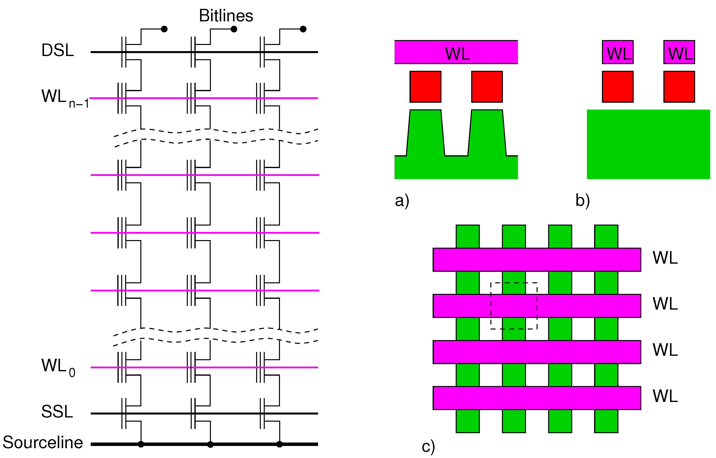

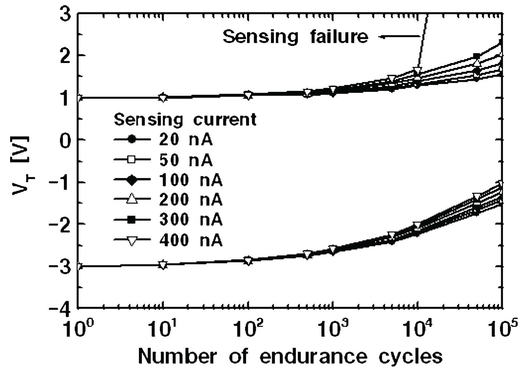
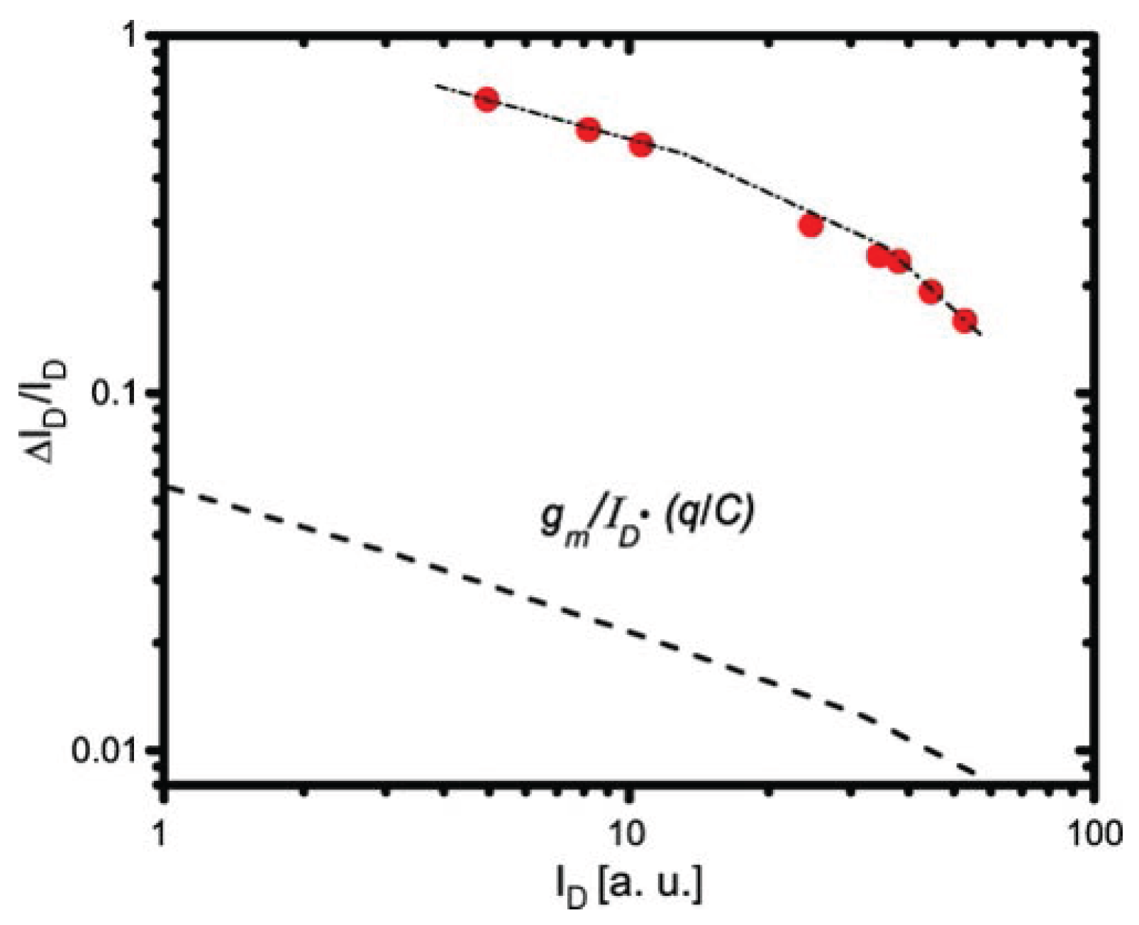
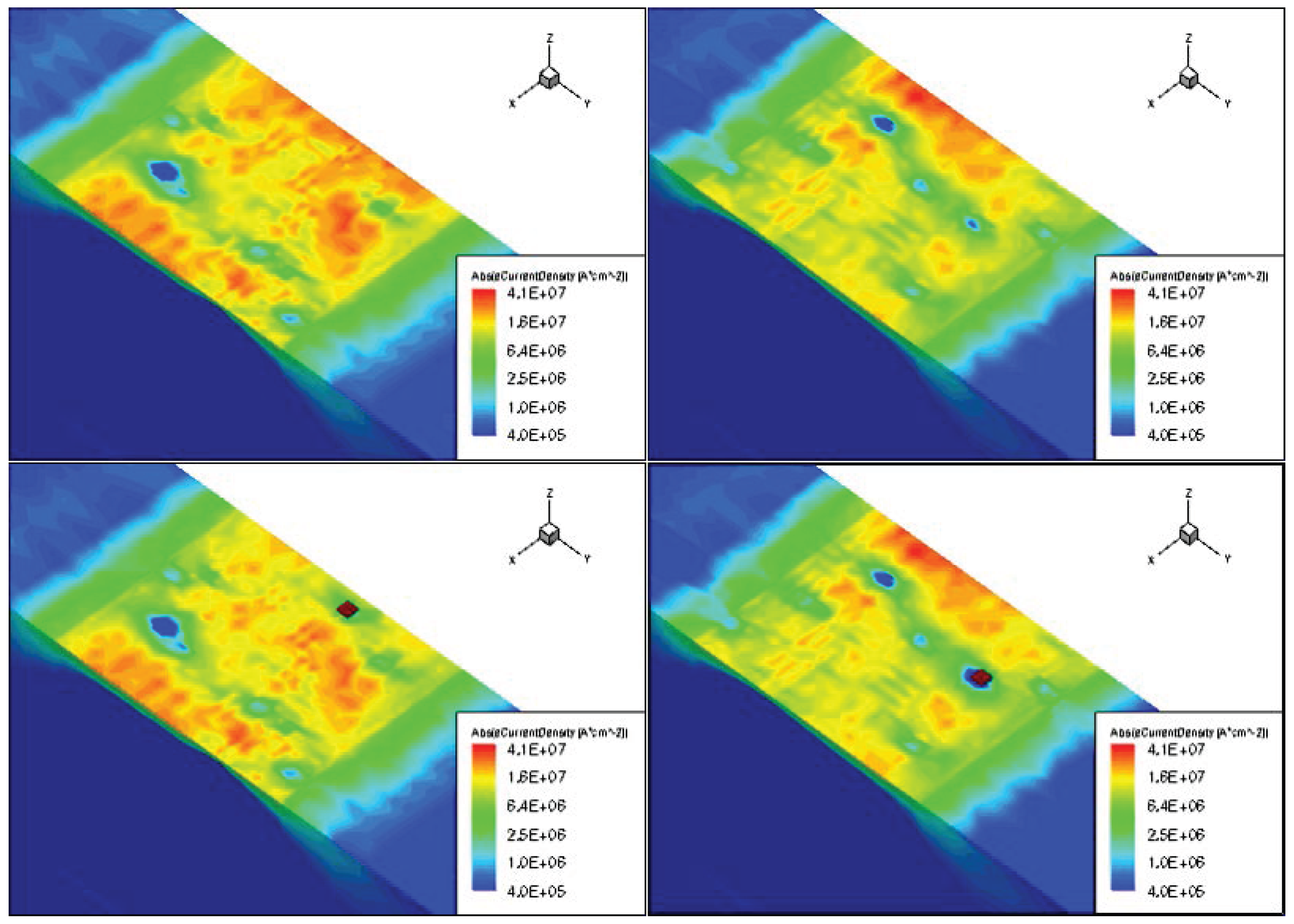
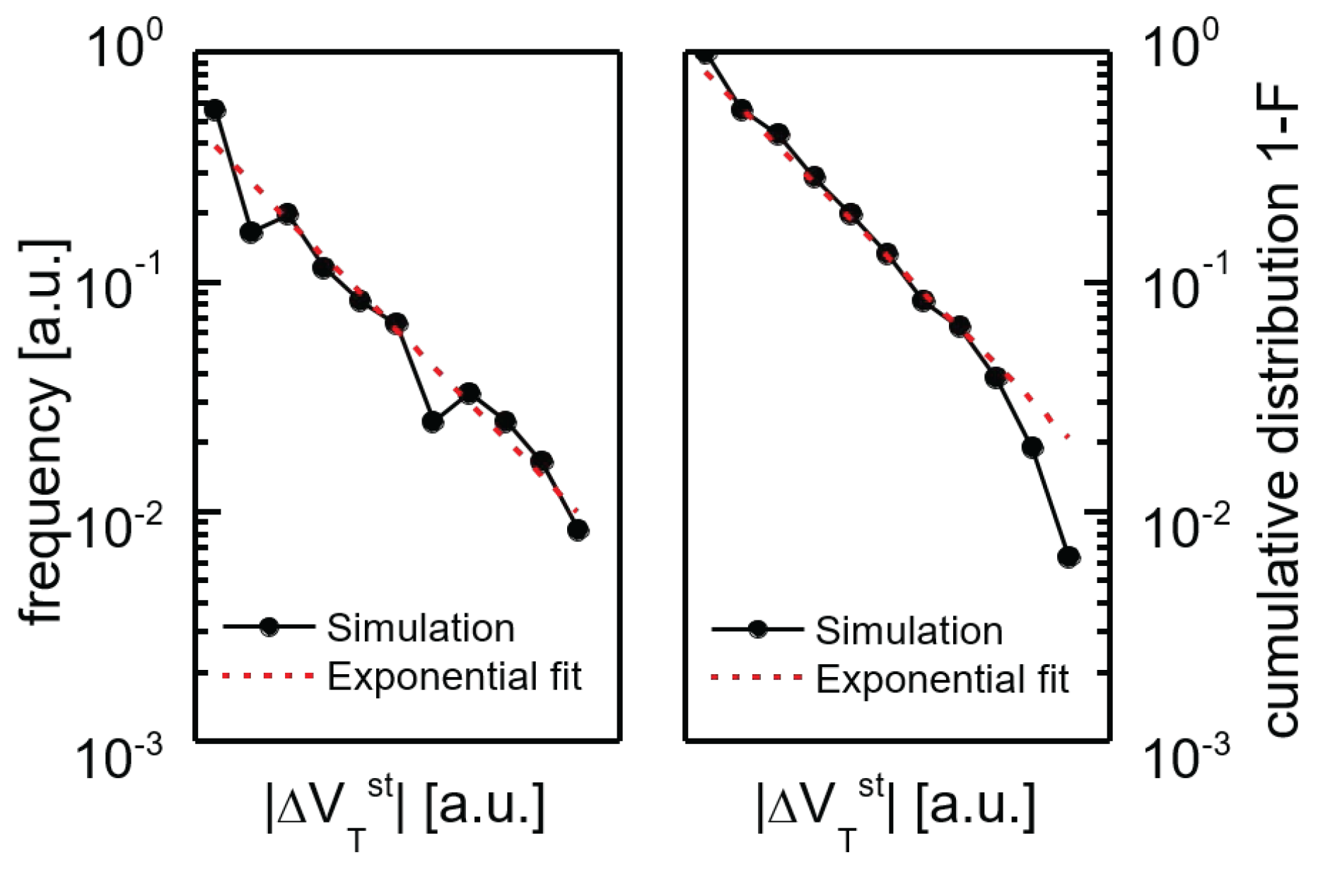

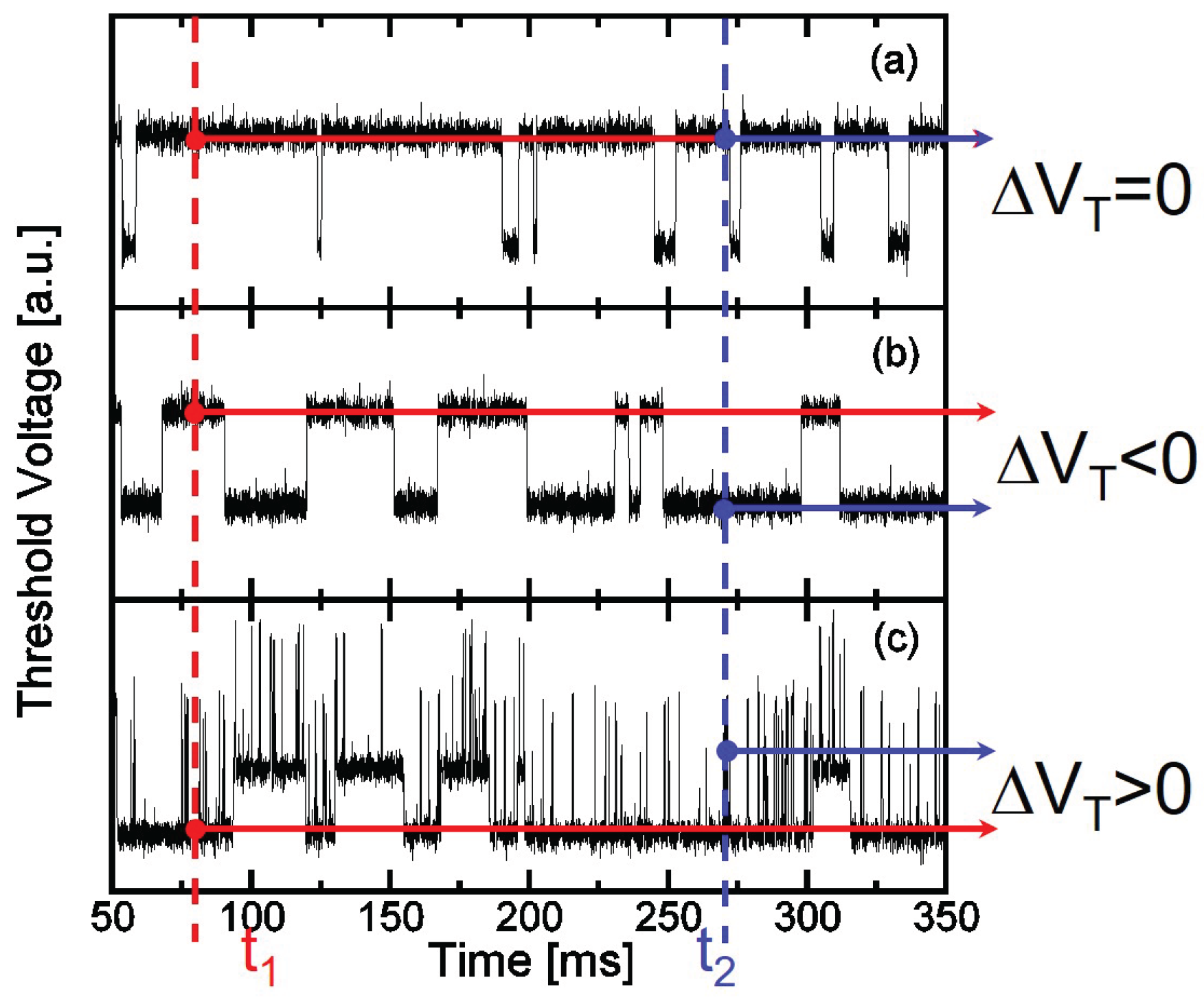

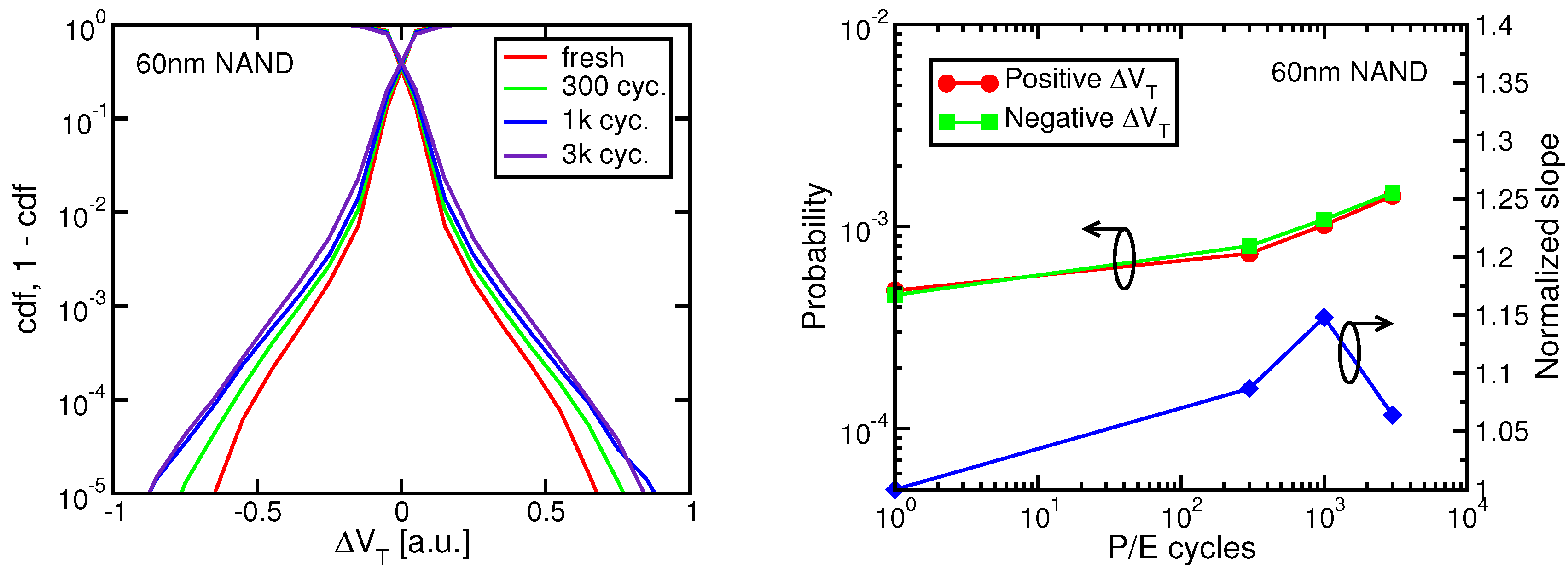


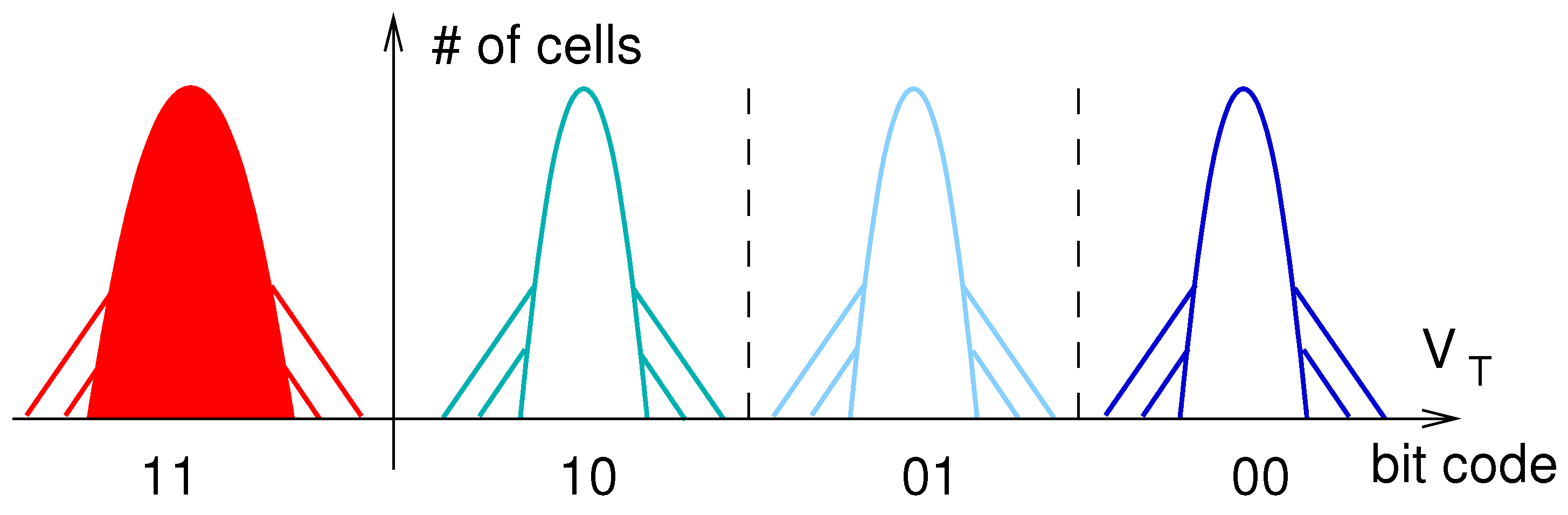


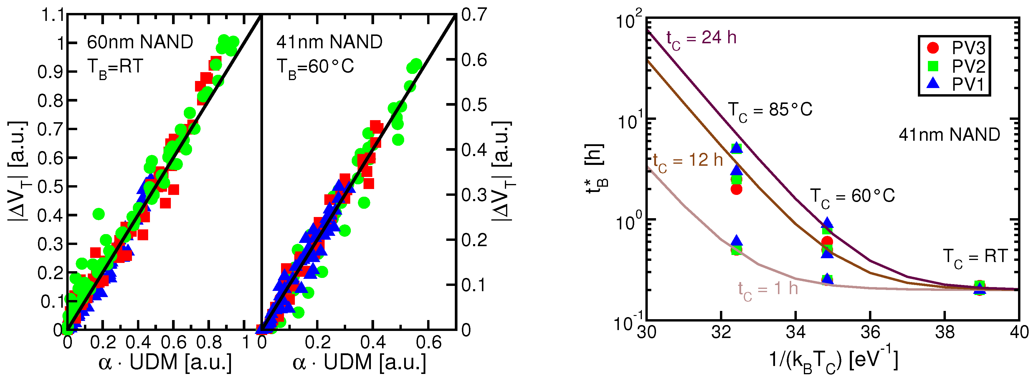

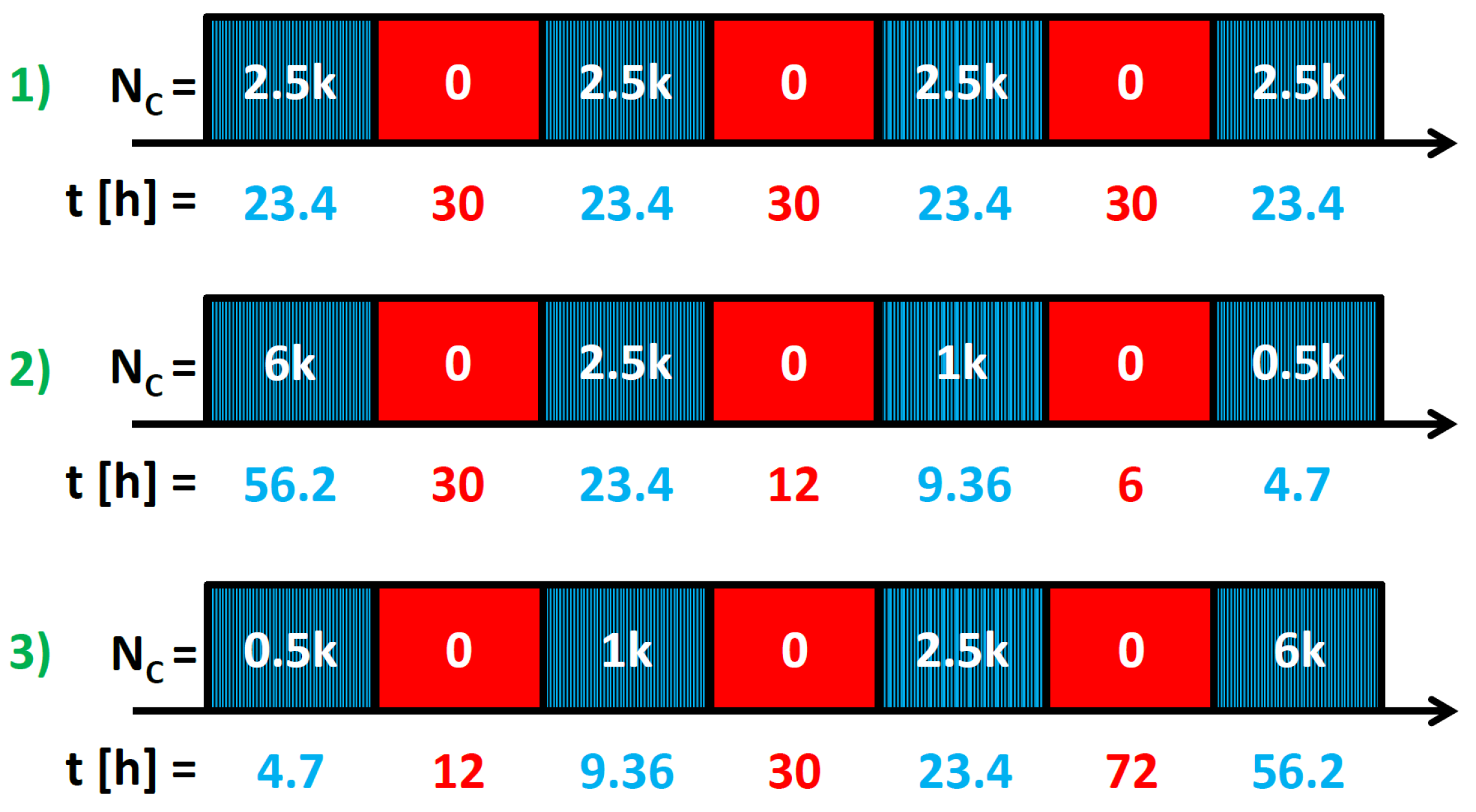

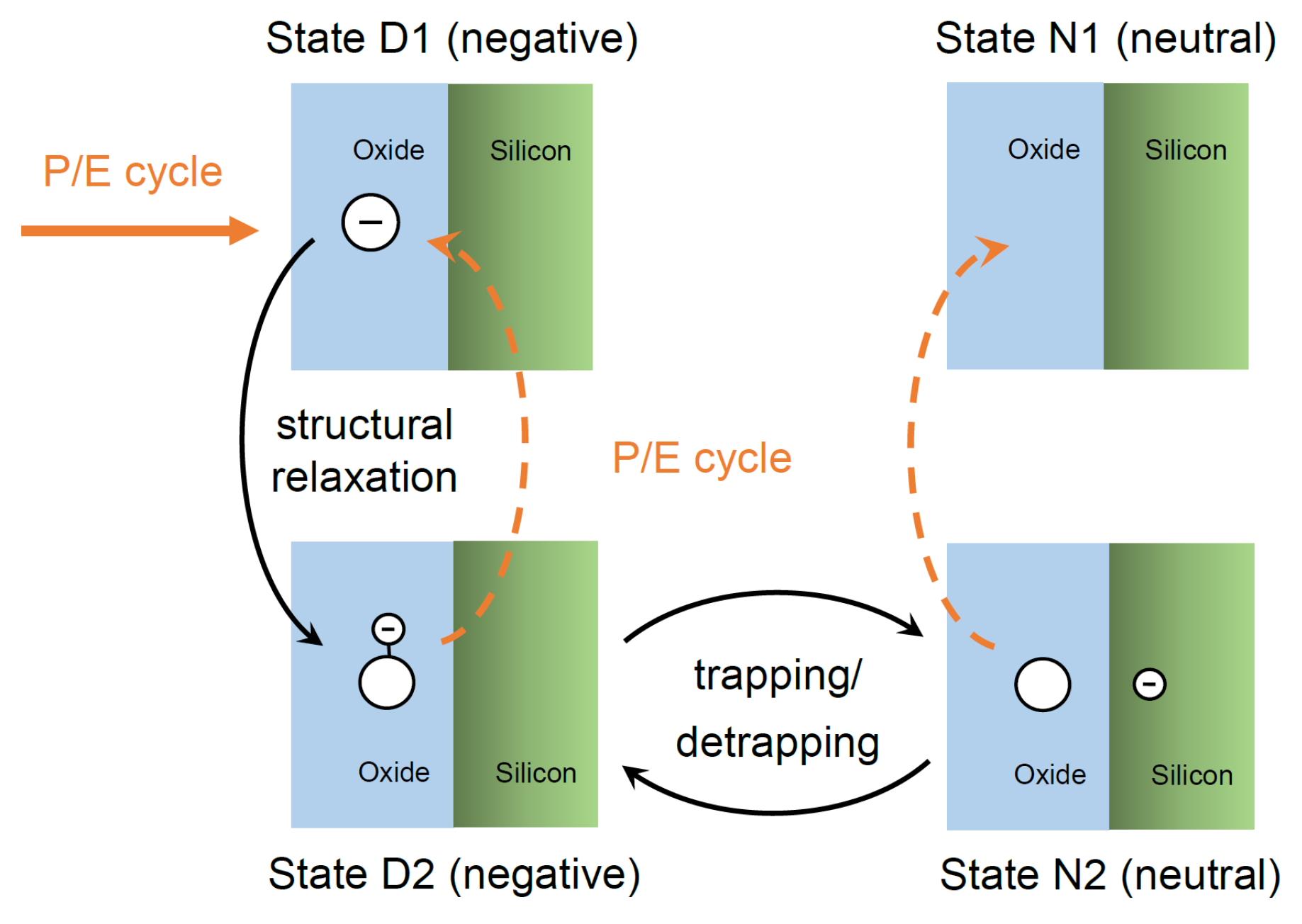
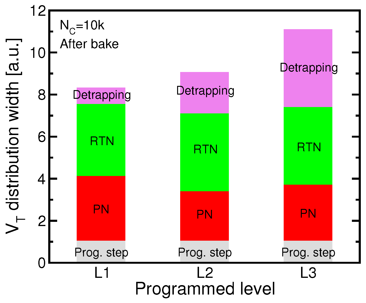

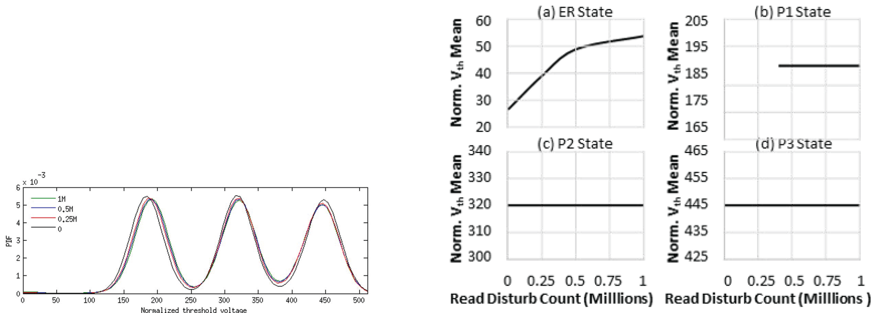


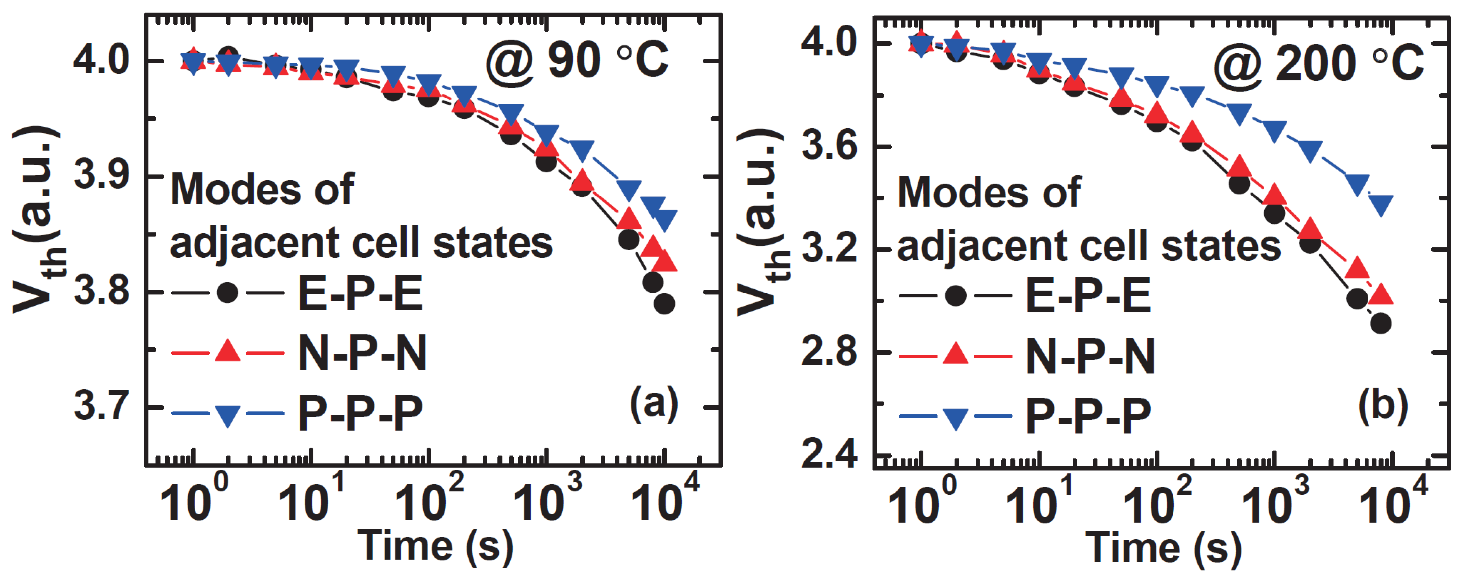
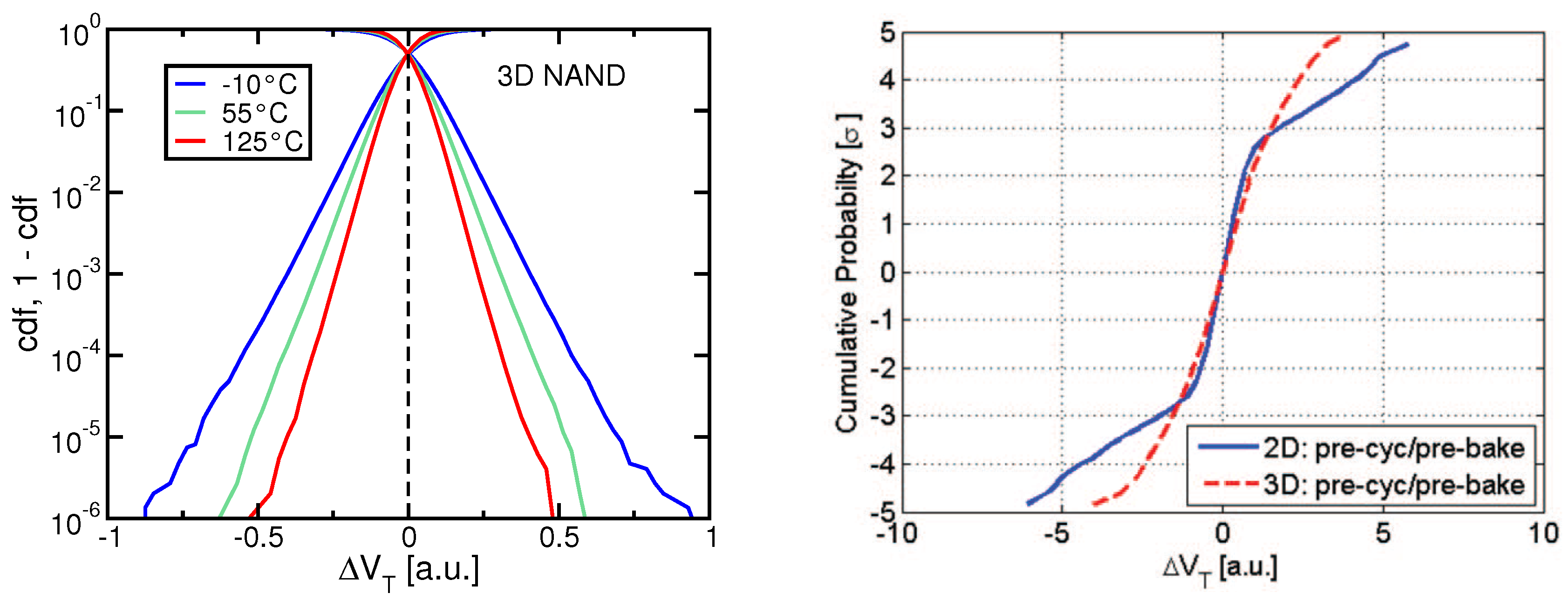


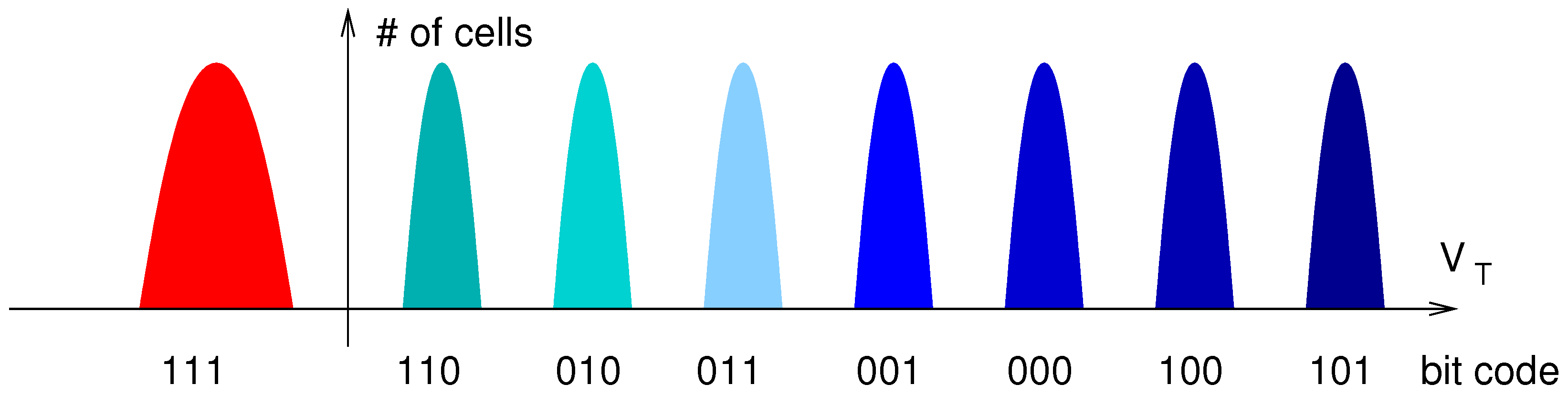
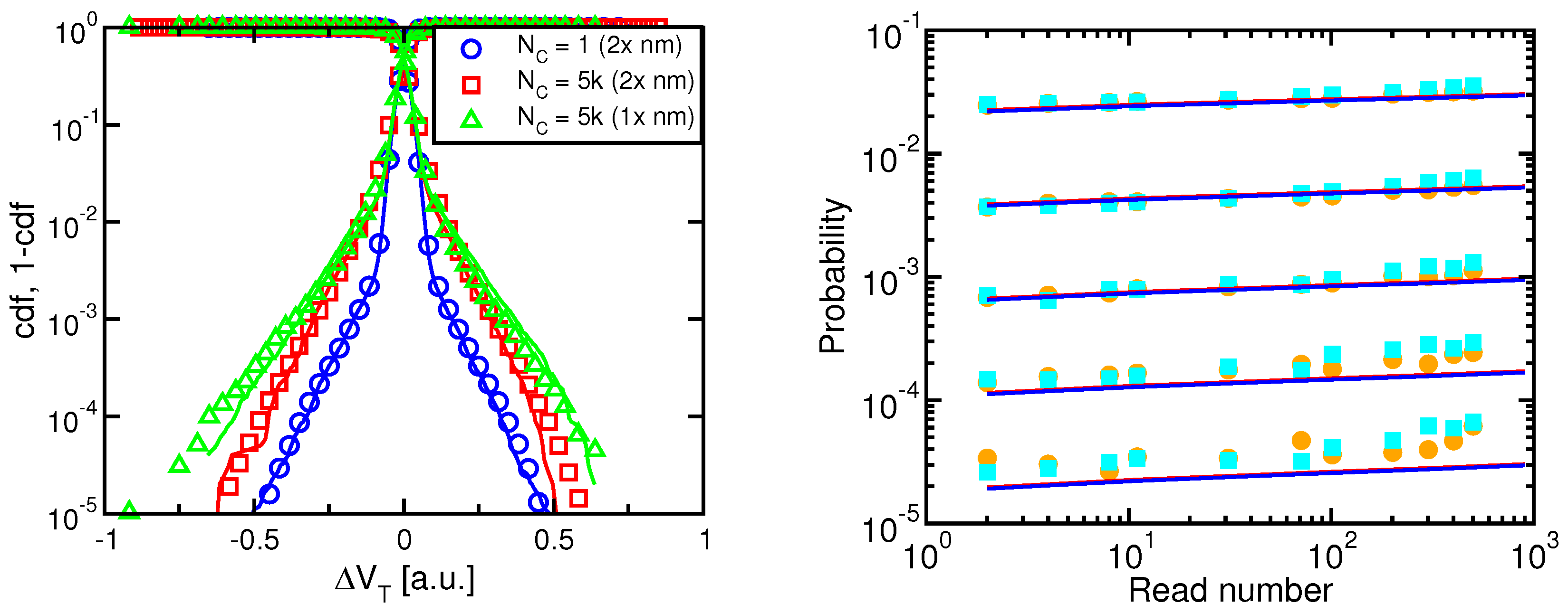
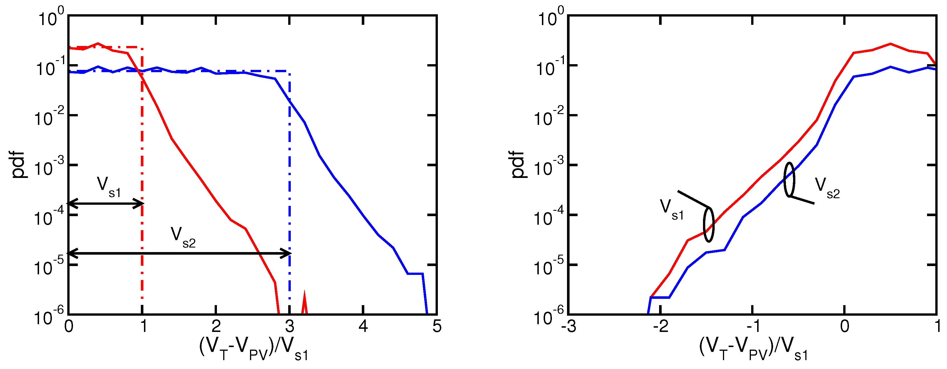
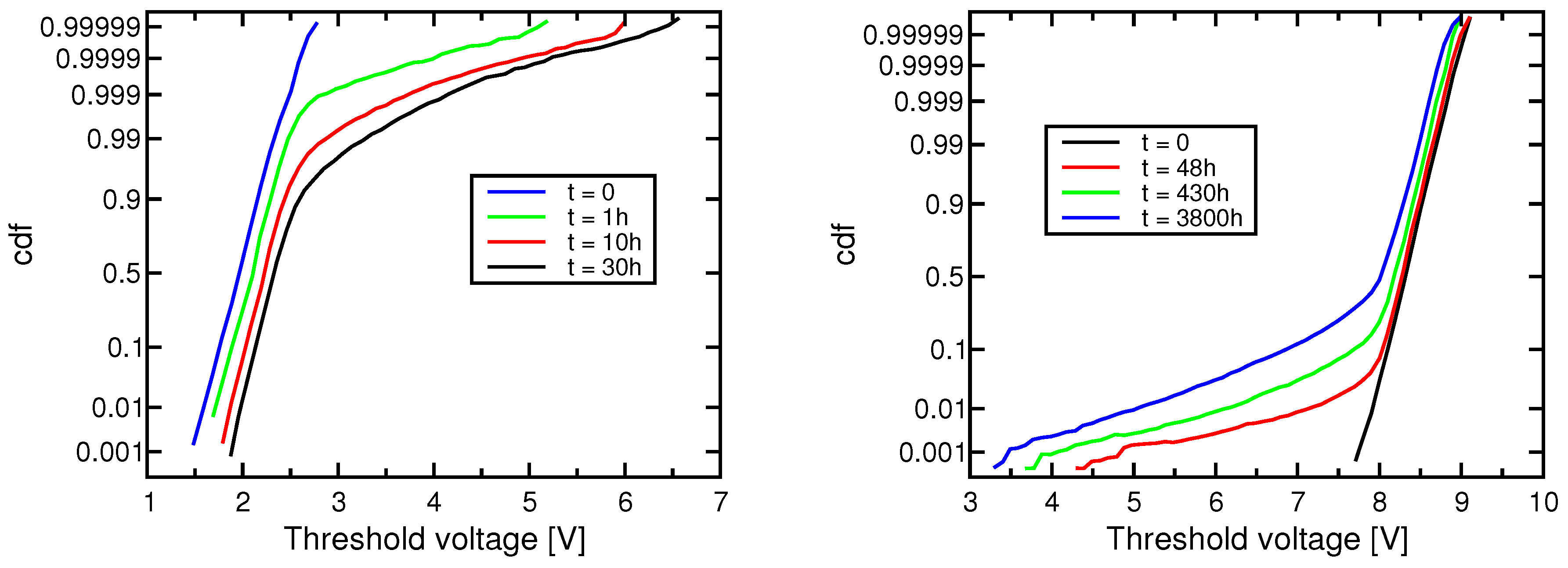
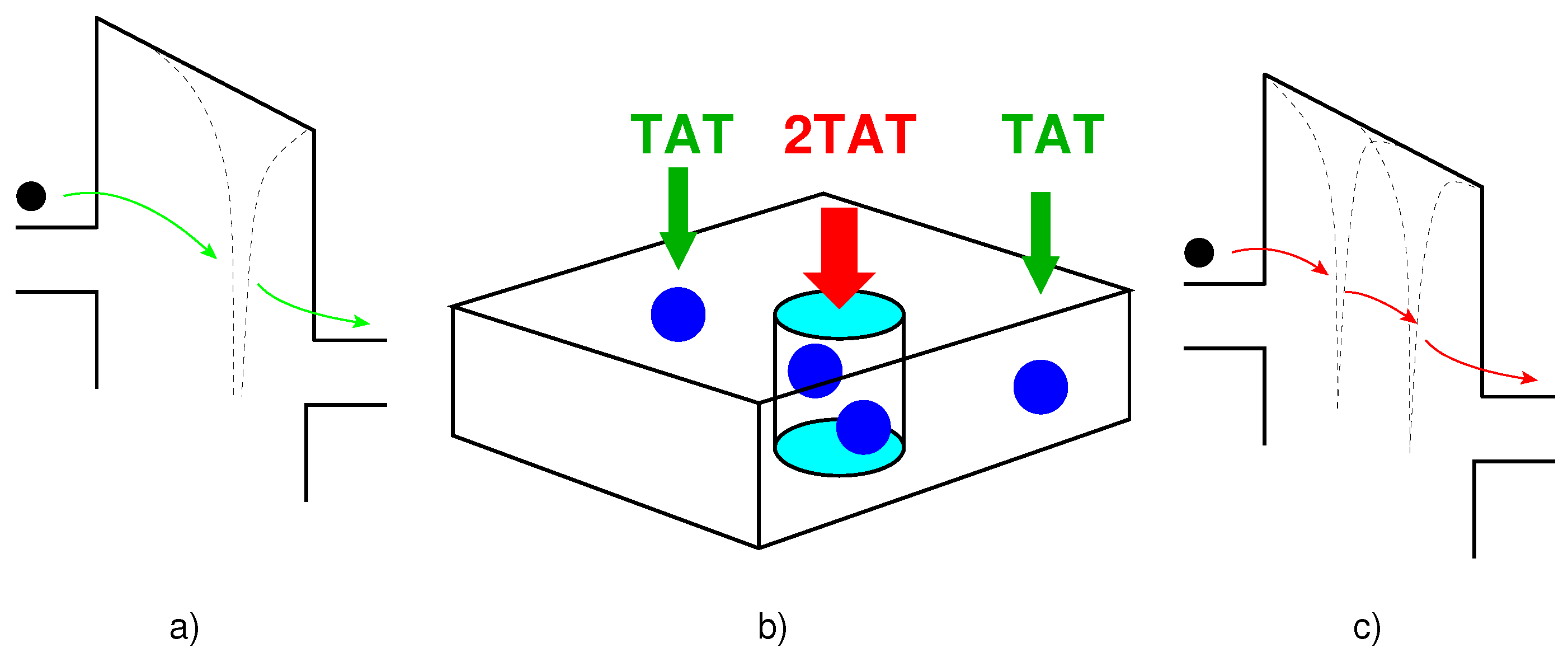
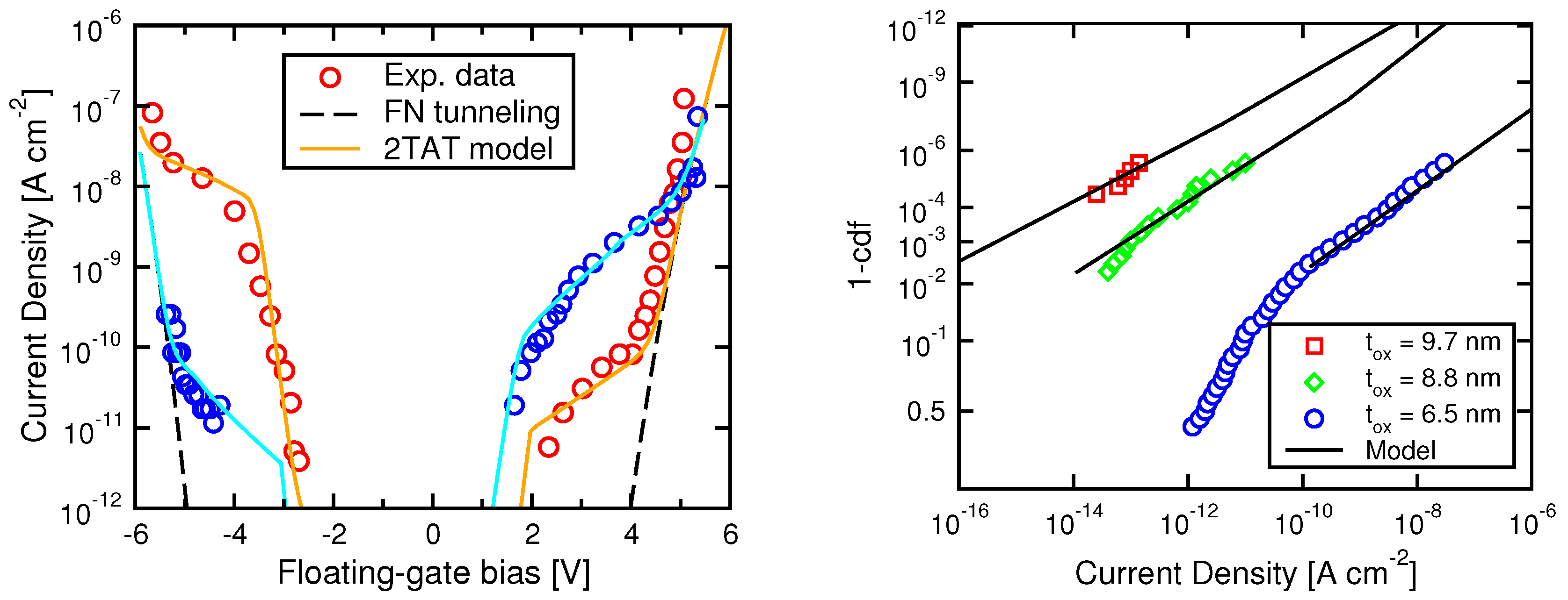
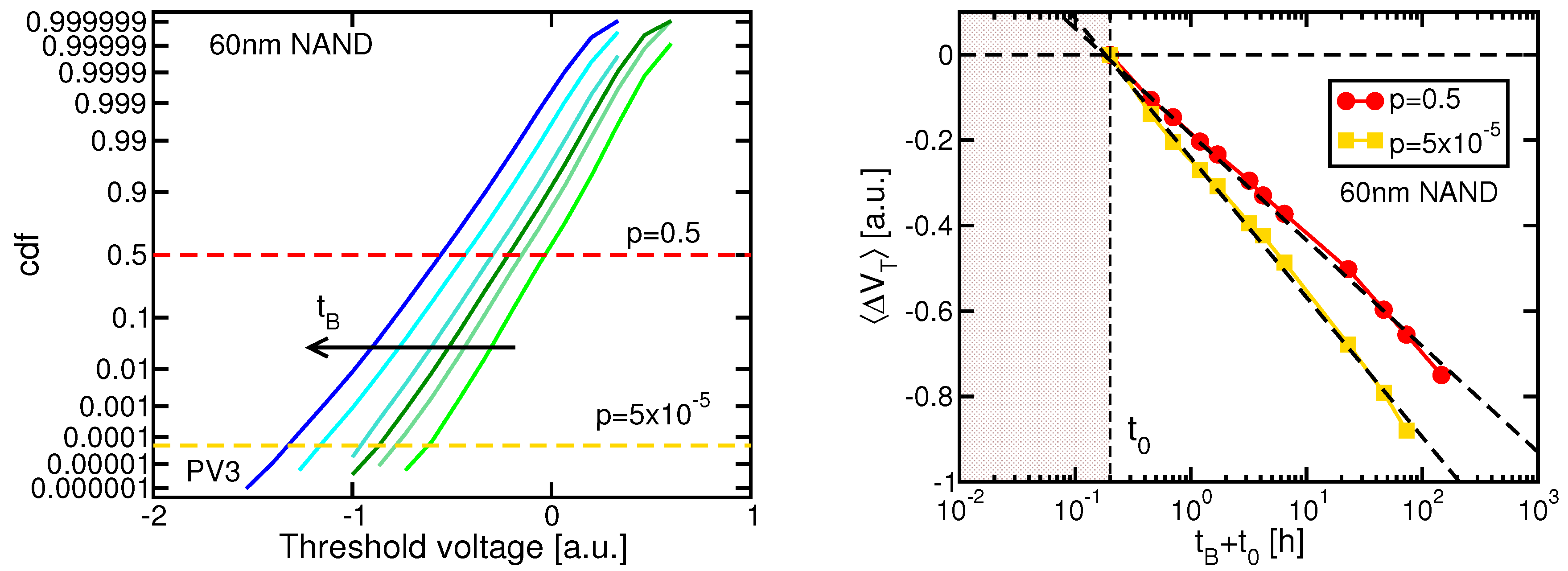
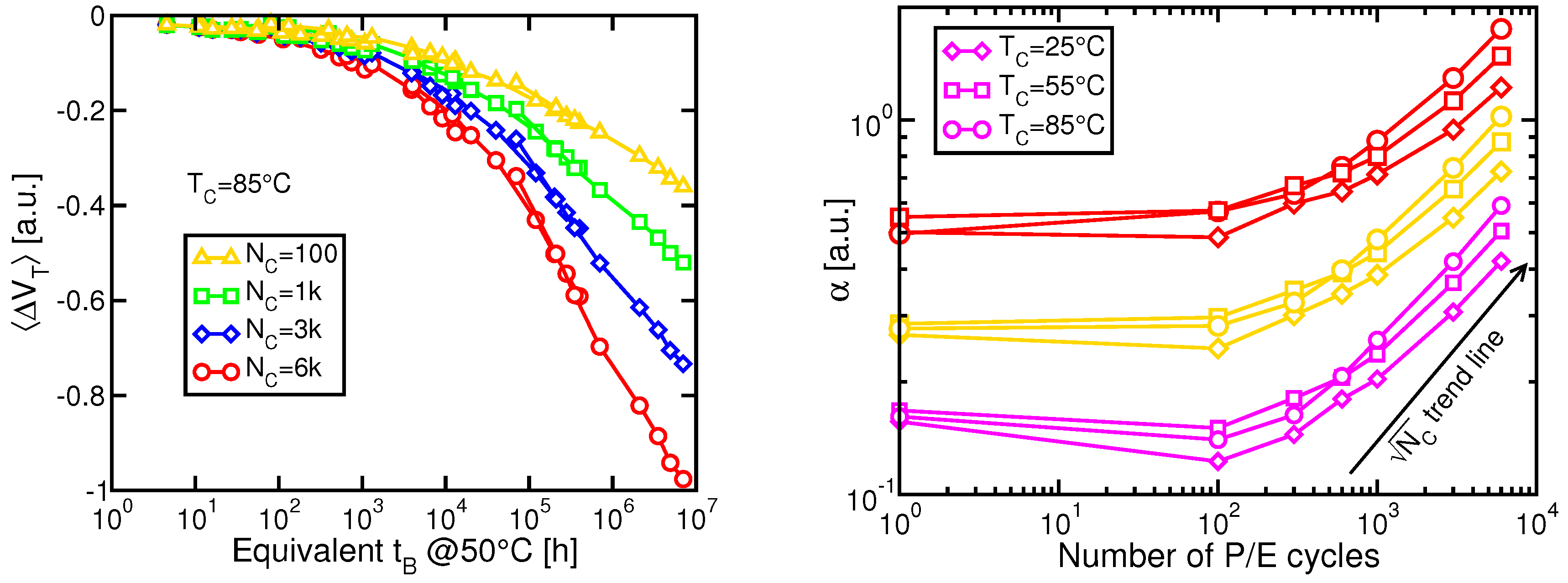
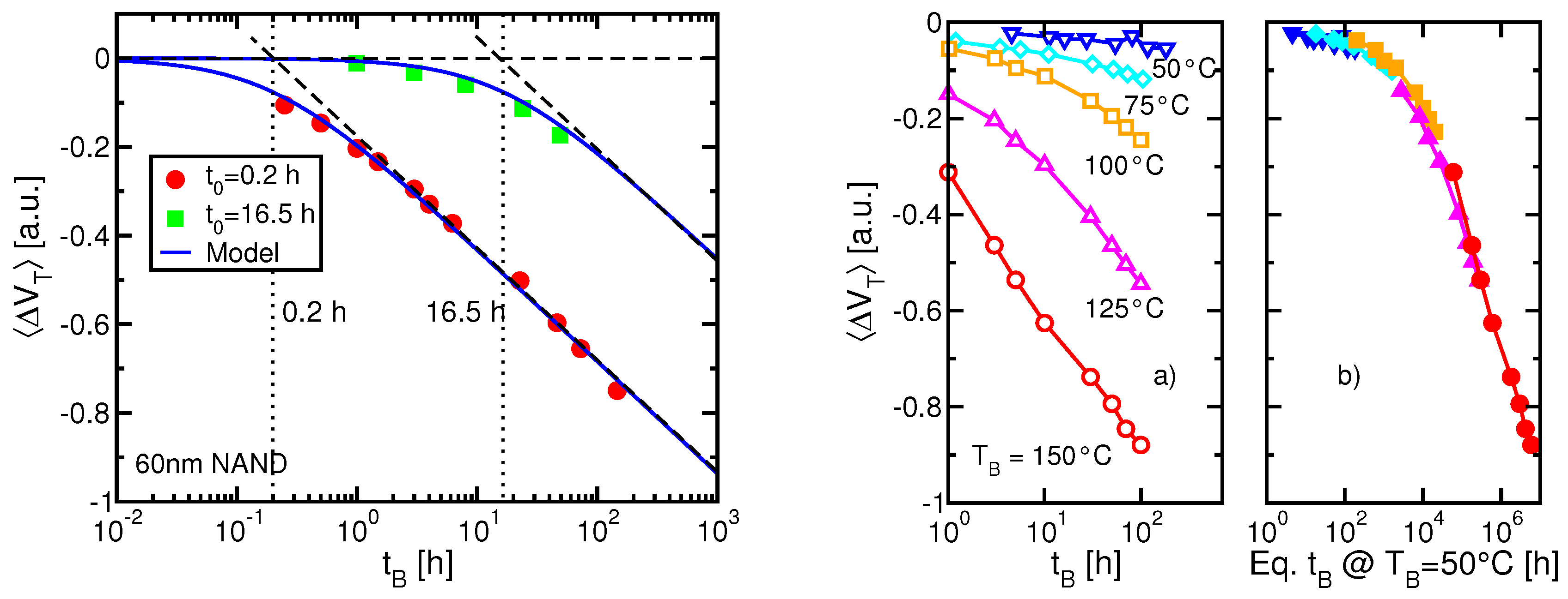
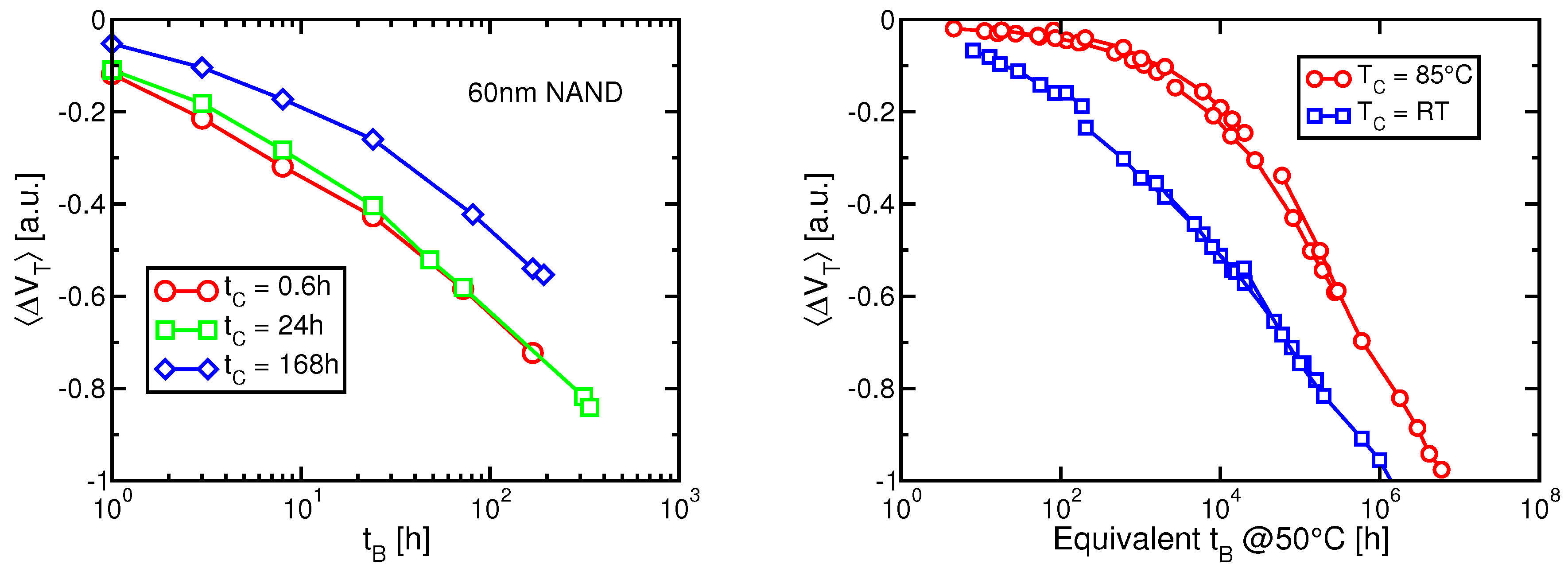
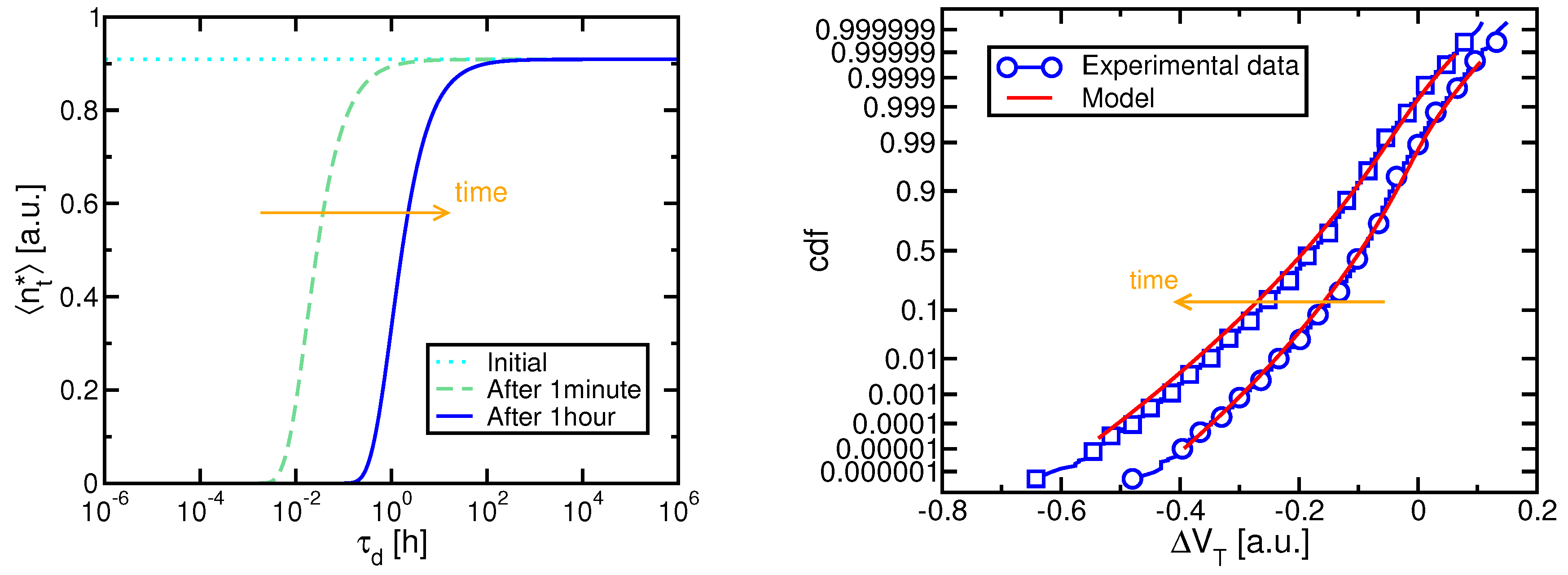
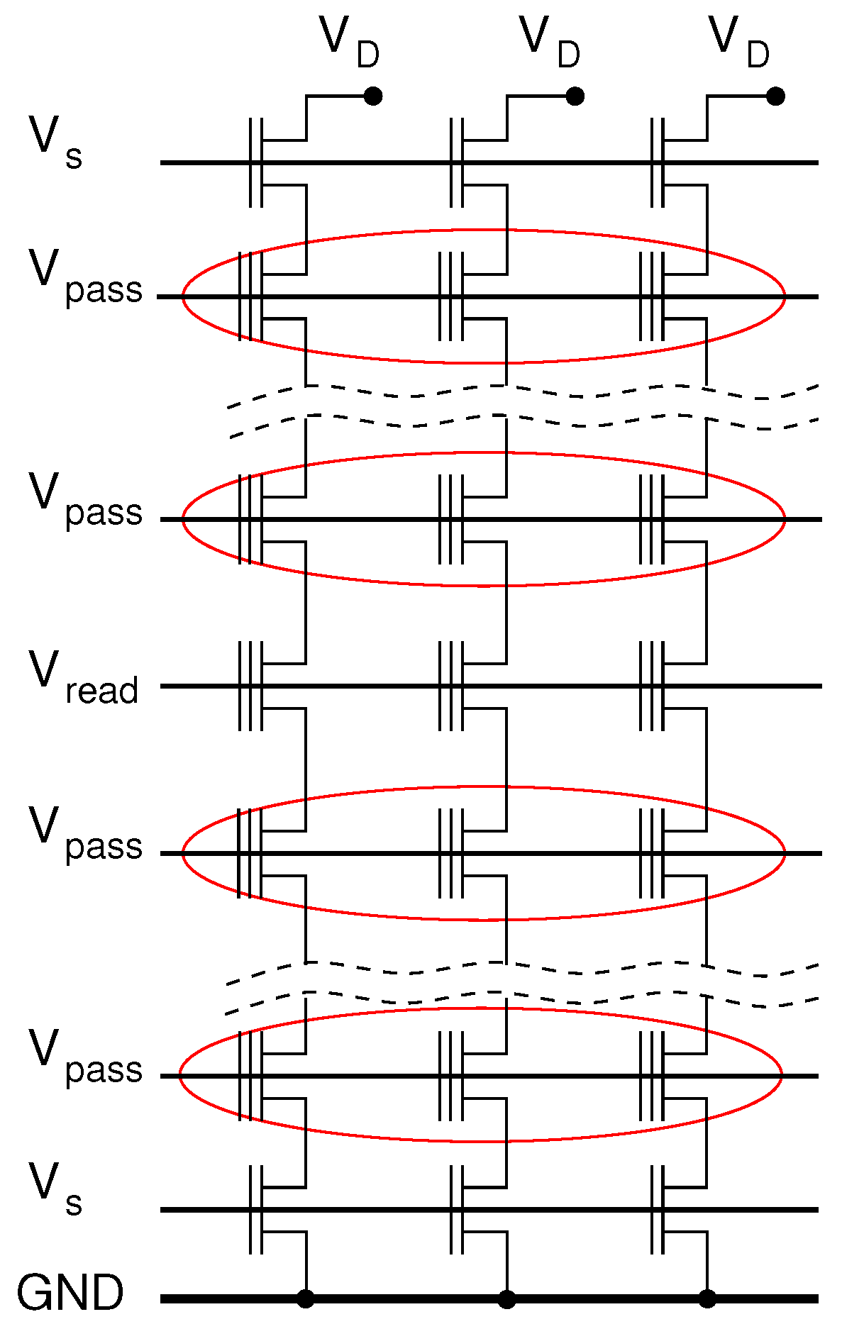
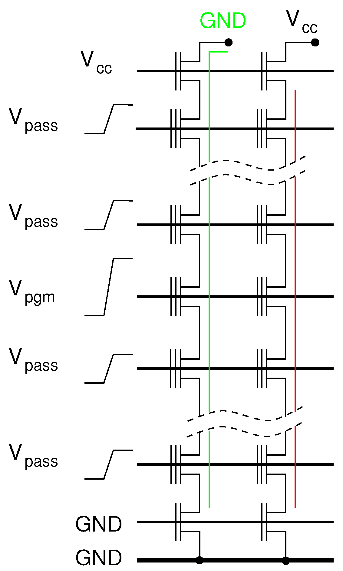
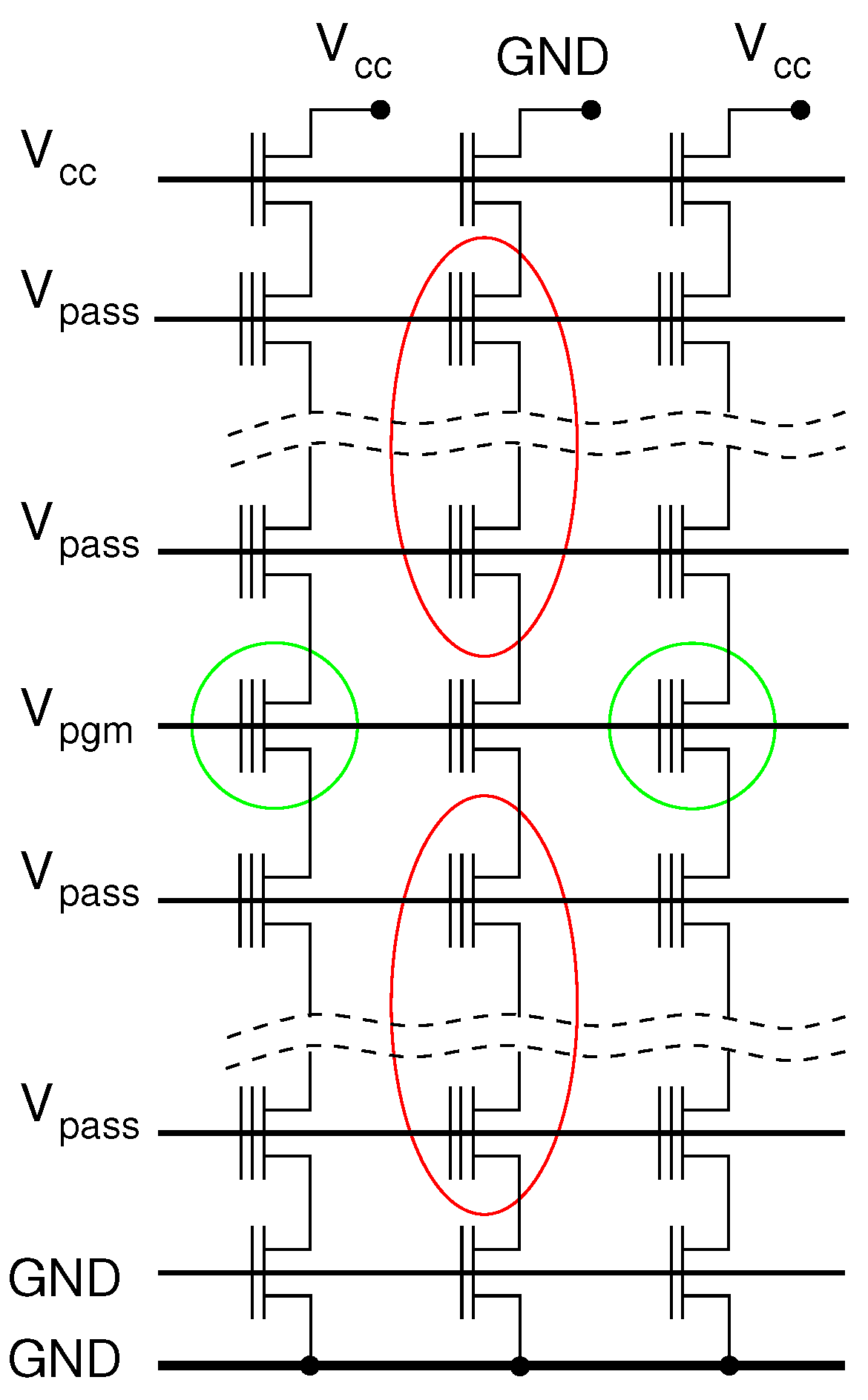
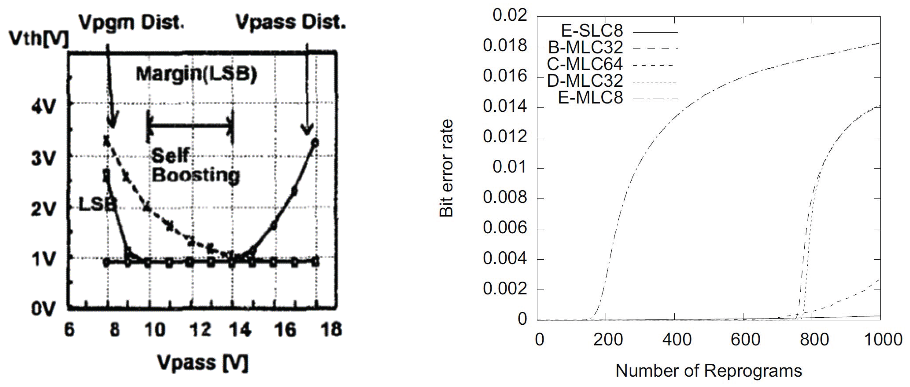
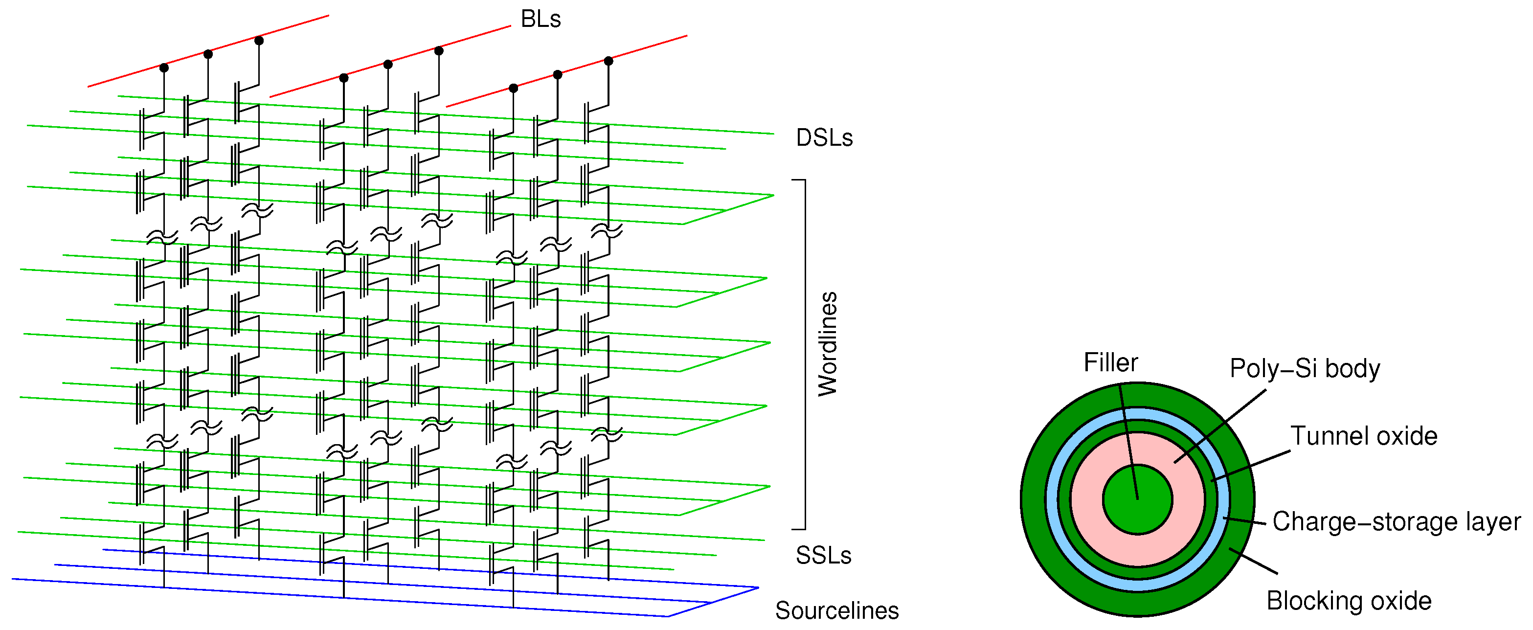
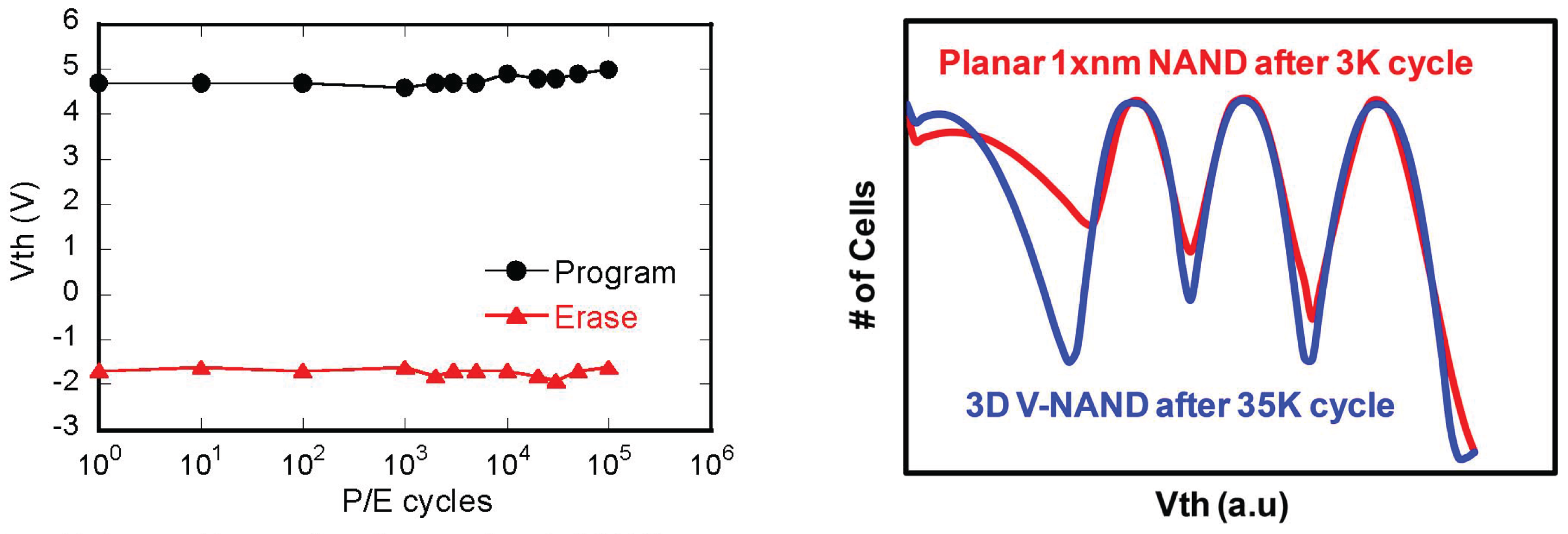
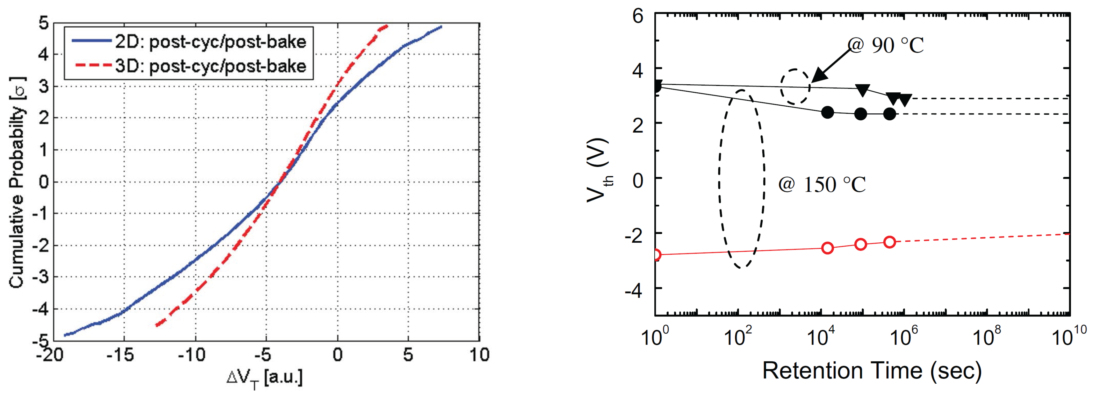
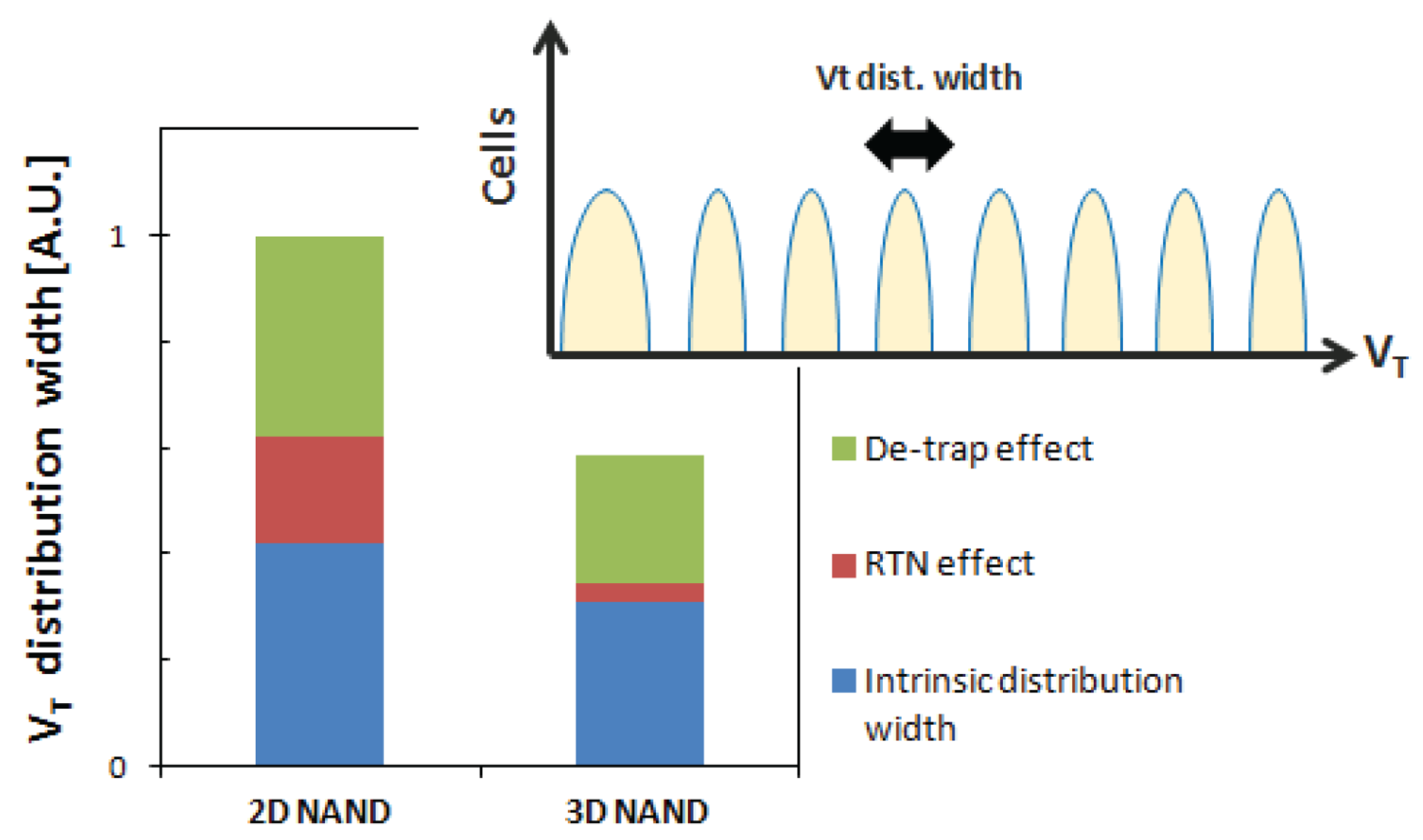
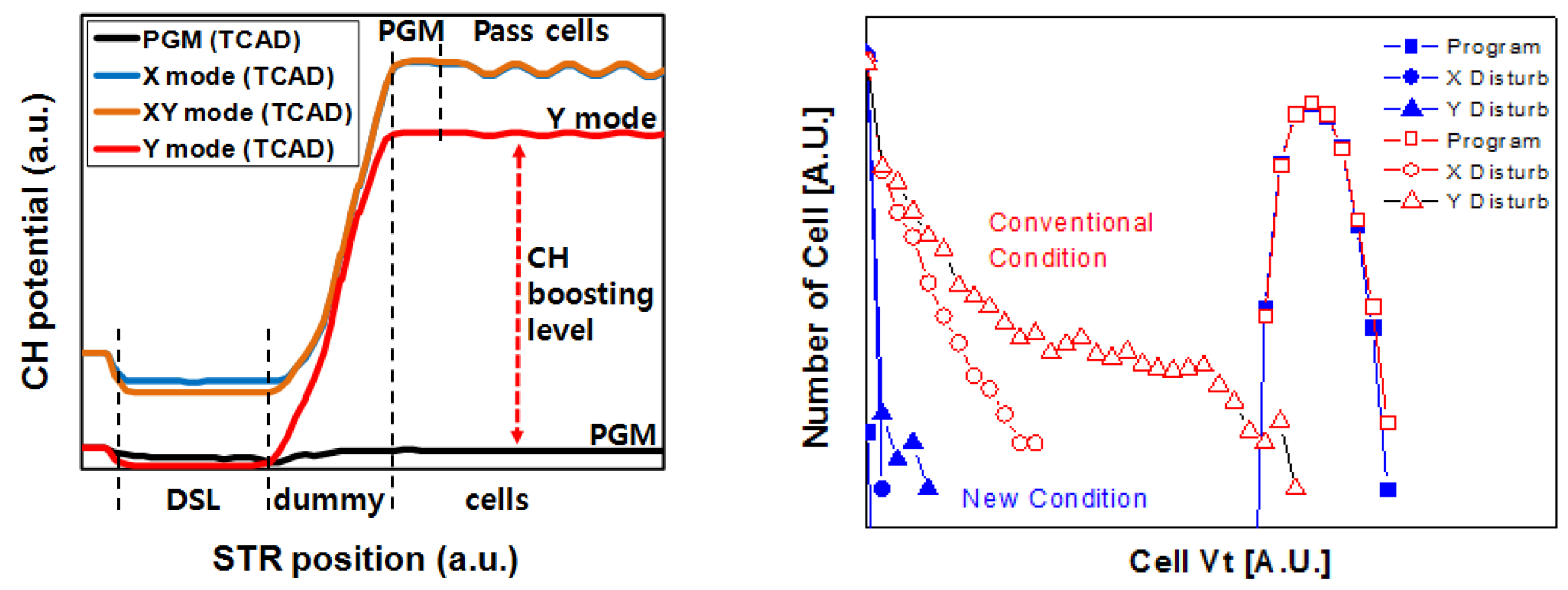
© 2017 by the authors. Licensee MDPI, Basel, Switzerland. This article is an open access article distributed under the terms and conditions of the Creative Commons Attribution (CC BY) license (http://creativecommons.org/licenses/by/4.0/).
Share and Cite
Spinelli, A.S.; Compagnoni, C.M.; Lacaita, A.L. Reliability of NAND Flash Memories: Planar Cells and Emerging Issues in 3D Devices. Computers 2017, 6, 16. https://doi.org/10.3390/computers6020016
Spinelli AS, Compagnoni CM, Lacaita AL. Reliability of NAND Flash Memories: Planar Cells and Emerging Issues in 3D Devices. Computers. 2017; 6(2):16. https://doi.org/10.3390/computers6020016
Chicago/Turabian StyleSpinelli, Alessandro S., Christian Monzio Compagnoni, and Andrea L. Lacaita. 2017. "Reliability of NAND Flash Memories: Planar Cells and Emerging Issues in 3D Devices" Computers 6, no. 2: 16. https://doi.org/10.3390/computers6020016
APA StyleSpinelli, A. S., Compagnoni, C. M., & Lacaita, A. L. (2017). Reliability of NAND Flash Memories: Planar Cells and Emerging Issues in 3D Devices. Computers, 6(2), 16. https://doi.org/10.3390/computers6020016