Architectural and Integration Options for 3D NAND Flash Memories


1
Dipartimento di Ingegneria (DE), Università degli Studi di Ferrara, Via G. Saragat 1, 44122 Ferrara, Italy
2
Microsemi Corporation, 20871 Vimercate, Italy
*
Author to whom correspondence should be addressed.
Computers 2017, 6(3), 27; https://doi.org/10.3390/computers6030027
Submission received: 31 July 2017
/
Revised: 7 August 2017
/
Accepted: 8 August 2017
/
Published: 10 August 2017
(This article belongs to the Special Issue 3D Flash Memories)
Abstract
:Nowadays, NAND Flash technology is everywhere, since it is the core of the code and data storage in mobile and embedded applications; moreover, its market share is exploding with Solid-State-Drives (SSDs), which are replacing Hard Disk Drives (HDDs) in consumer and enterprise scenarios. To keep the evolutionary pace of the technology, NAND Flash must scale aggressively in terms of bit cost. When approaching ultra-scaled technologies, planar NAND is hitting a wall: both academia researchers and industry worked to cope with this issue for several decades. Then, the 3D integration approach turned out to be the definitive alternative by eventually reaching mass production. This review paper exposes several 3D NAND Flash memory technologies, along with their related integration challenges, by showing their different layouts, scaling trends and performance/reliability features.
1. Introduction
NAND Flash memory technology is currently the state-of-the-art solution for every platform requiring storage, ranging from embedded solutions up to Solid State Drive (SSD) applications. Planar technology is hitting several integration roadblocks due to the fundamental limitations of the feature size shrinking. In the last few years, process solutions like double patterning lithography techniques and algorithmic solutions like the electrostatic interference control between neighbor cells [1] were explored to overcome those issues. However, there is still a number of intrinsic phenomena that prevent the scaling of planar integrated cells. Among them, the random doping fluctuations [2], the random telegraph noise [3] and the electron injection statistics [4] significantly reduce the margin between the threshold voltage distributions. Multi-bits per cell storage paradigms have further exacerbated those issues, with the consequent effect of reducing the reliability of the memory in terms of endurance (i.e., sustainable write/erase cycles before a failure) and data retention properties.
3D NAND Flash architectures represent an opportunity to overcome the limitations of planar technology. To this extent, many efforts were spent both in research and development of a suitable platform that can address at the same time: reduced fabrication costs, easy-to-reach high yield for mass production, high storage density enabled by the multi-bits per cell approach and full compliance with legacy NAND Flash specifications for interfacing with existing systems.
The paradigm shift enabling 3D NAND Flash revolution was the transitioning from the Floating Gate (FG) technology to the Charge Trapping (CT) for the cell transistors [1]. Most architectures presented so far rely on CT cells, although there are some exceptions like FG-based 3D NAND Flash architectures [5,6].
In this paper, we will mainly discuss 3D NAND Flash architectures based on the CT process option, although FG cells are considered for peculiar architectures. A topological classification of different integration solutions with an estimate of the process costs and of the electrical performances will be provided by considering the following cases:
- Control gate and channel along the horizontal direction;
- Control gate along the horizontal direction and channel along the vertical direction.
In the first category, we will review the so-called 3D stacked option, which is the preliminary attempt to achieve 3D integration starting from planar technology [7]. In the second category, we will provide the description of several architectures like: the Bit Cost Scalable (BiCS) presented for the first time by Toshiba [8,9], its improved version, namely the Pipe-shaped Bit Cost Scalable (P-BiCS) [10,11], and the pathway to the V-NAND architecture from Samsung [12,13] ranging from the Vertical Recess Array Transistor (VRAT) [14], the Vertical Stacked Array Transistor (VSAT) [15], and the Terabit Cell Array Transistor (TCAT) [16].
2. 3D Stacked Architecture
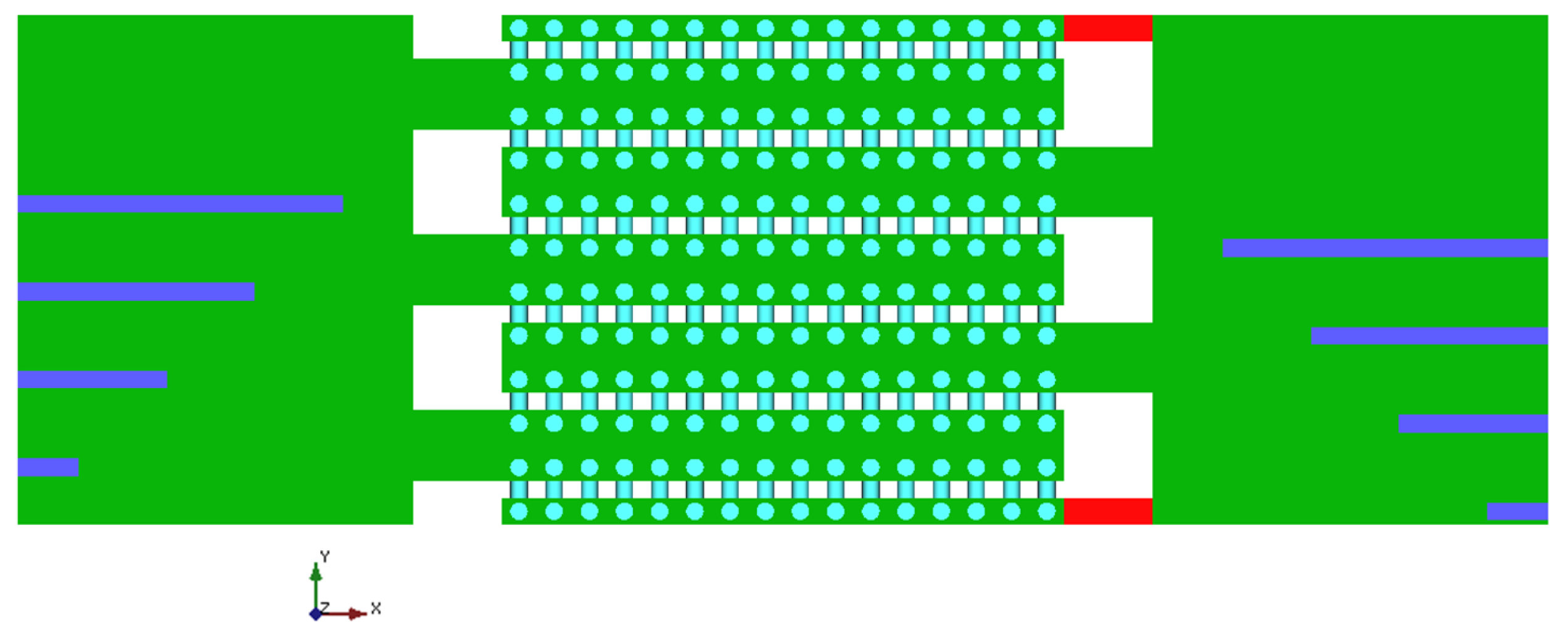
The first attempt to reach the manufacturing of a 3D NAND Flash architecture explored the straightforward idea to stack multiple planar memory arrays [17]. Figure 1 shows a bird’s eye view of a 3D stacked NAND Flash integrating two separate planes. In here, drain and bitline contacts are shared between NAND strings belonging to different layers, whereas source/wordline contacts and source/drain selectors are associated to separate layers.
Cost and process technologies considerations of this architecture can be derived from those of the planar products. From a purely technological standpoint, the major hurdle is represented by the thermal budget of the manufacturing process to grow and populate additional layers. Indeed, to minimize the bottom layer degradation of its reliability features and to provide uniformity in performance characteristics among memory cells, that parameter should be kept rather limited. The biggest advantage of the 3D stacked architecture lies in the flexibility since each layer is manufactured separately [17]. A substantial difference between this architecture and the planar NAND Flash is the presence of a floating substrate, which constrains the erase operation.
The economical assessment of the 3D stacked integration option proves its ineffectiveness since it multiplies the planar array fabrication costs by the number of layers foreseen in the product. A minimal cost improvement is in the shared peripheral circuits and metal interconnections of the array. The major works on this architecture were described in [18,19], although leveraging on CT cells.
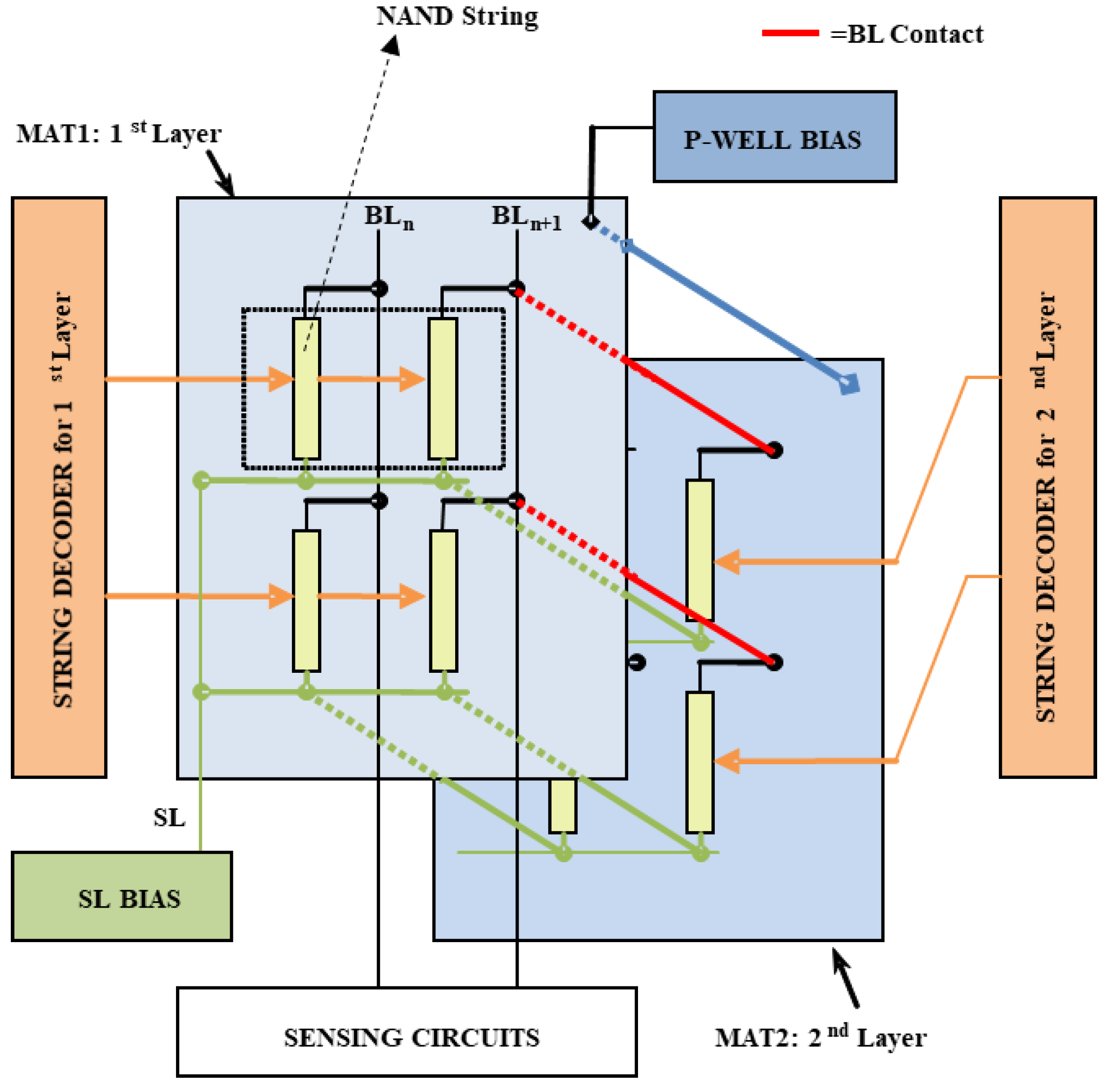
In [7], a two-layer 3D stacked NAND Flash built entirely from a planar process has been described, as shown in Figure 2. On the first layer (i.e., indicated as MAT1 in Figure 2 where MAT stands for matrix), the memory array and also the peripheral circuitry are present, whereas the second layer (MAT2) is only for the array. Metal bitlines contact both layers using vias. Since the bitlines are shared, the sensing can be performed with a minimal burden on the capacitive load; therefore, the only penalty in timings and power consumption is ascribed to the vias [17]. String decoders are independent, allowing safe operations in terms of layer disturbs.
As pointed out earlier in the paper, this memory concept allows operating independently on each layer, although a proper biasing scheme is mandatory to avoid errors and reliability issues. Table 1 resumes the bias conditions of each layer for read, program and erase operations. The table assumes the architecture described in Figure 3 where MAT1 is the first layer that is currently selected for operation, MAT2 is the second layer, which is inhibited, BLn represents the shared bitline contact, BLS is the bitline selector, SLS is the source line selector, SL is the common source line contact and P-Well is the common p-doped silicon well bias for erase operation.
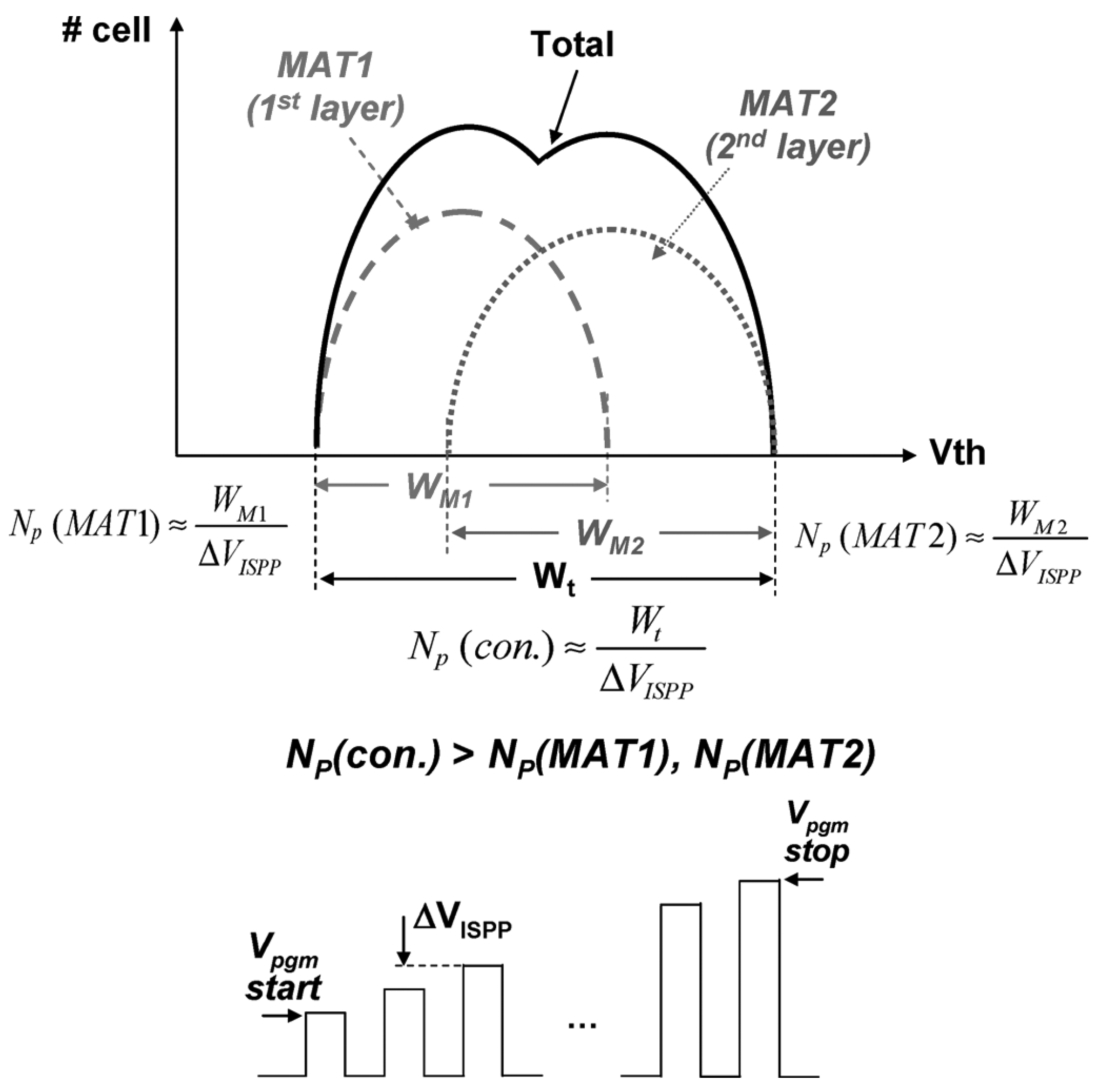
In this architecture, it is important to point out that since the layers are fabricated independently, there is a significant difference in the threshold voltage distributions after a program operation with the Incremental Step Pulse Program (ISPP) algorithm [20]. The resulting distribution has a width that comprises the width of the threshold voltage distribution for the first and the second layer, turning to the situation depicted in Figure 4. The enlargement of the programmed threshold voltage distribution yields a reduced performance caused by the higher number of program pulses supplied during ISPP and to a difficult control in multi-bit approaches. To this extent, in [7], a dedicated program scheme has been designed that compensates the ISPP per layer.
3. BiCS Architecture
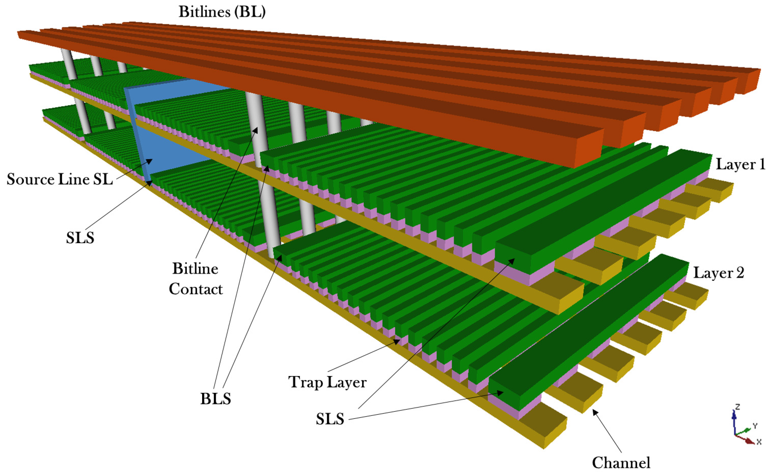
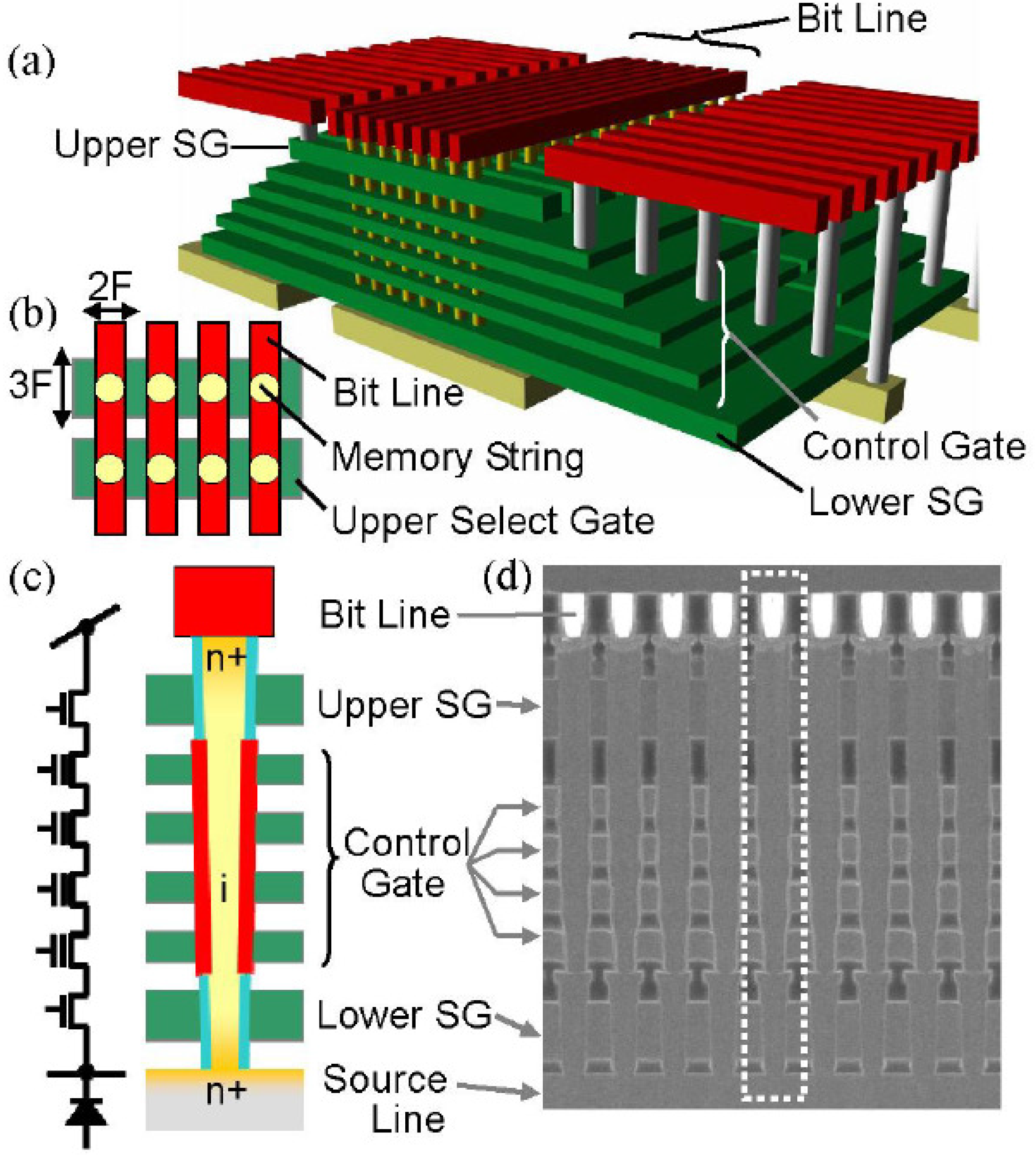
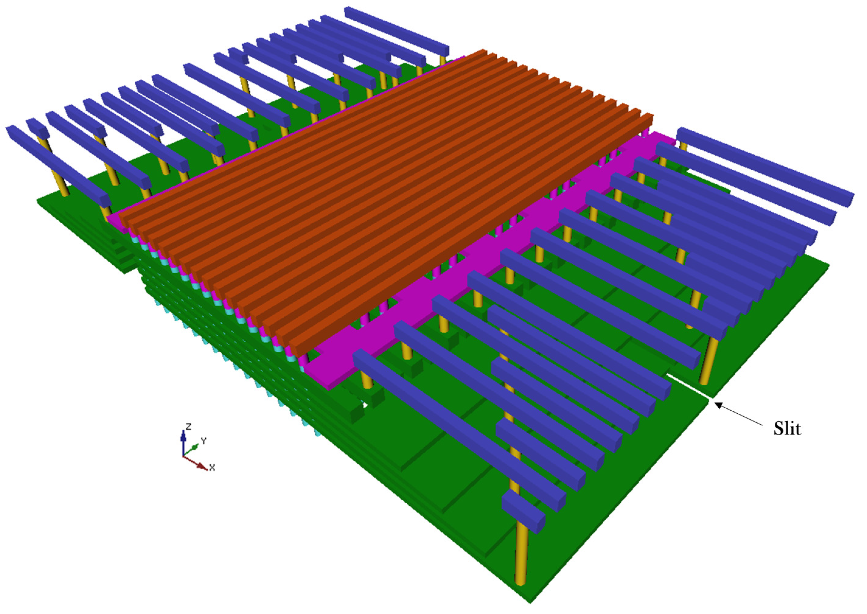
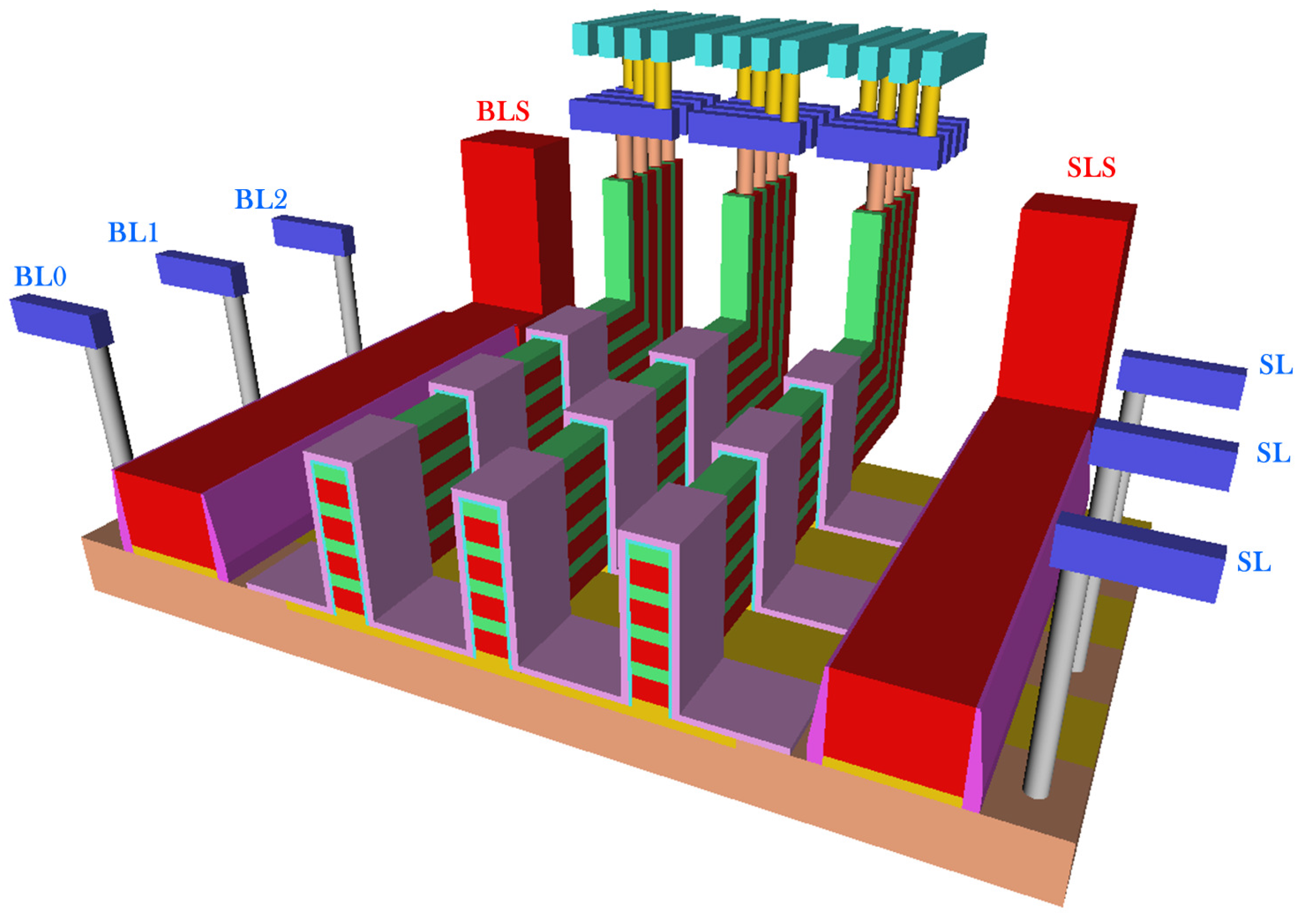
The BiCS 3D NAND Flash architecture is described in Figure 5 [8]. The first element of the architecture is the Control Gate (CG) stack shown by the different rectangle elements piled on top of each other, whereas the bottom rectangle plate is the ensemble of Source Line Selectors (SLS) terminating the Flash string. Multiple holes are drilled through the stacks and filled with poly-silicon in order to form a series of vertically-arranged NAND Flash memory cells. Bitline Selectors (BLS) and Bitlines (BL) contacts are on top of the structure [21]. Each cell in the BiCS architecture works in depletion-mode [22] since the poly-silicon constituting the body of the transistor is lightly n-doped with a uniform profile or even left un-doped. This reduces the manufacturing complexity of the p-n junction along the vertical direction of the plugs (also called pillars). The CG plate intersection with a pillar maps a single memory cell. Each NAND Flash string of cells is connected to a BL contact via BLS, whereas the bottom of the string is connected to a common source diffusion formed directly on the process substrate made of silicon.
The overall storage capacity and the bit density of the memory can be increased by adding CG plates. In this case, the number of lithography steps remains constant because the pillars’ drilling process can be achieved in a single process step [23].
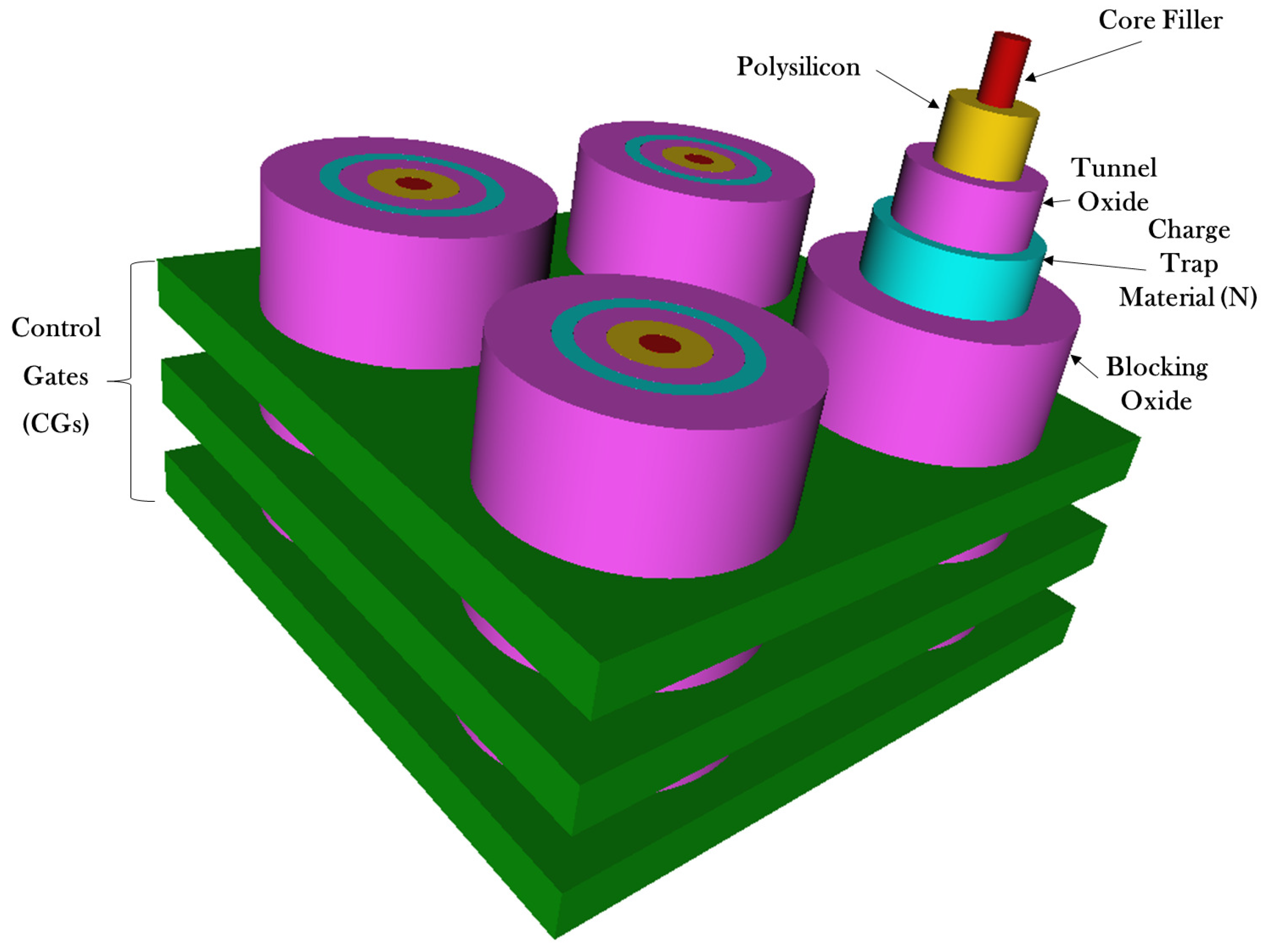
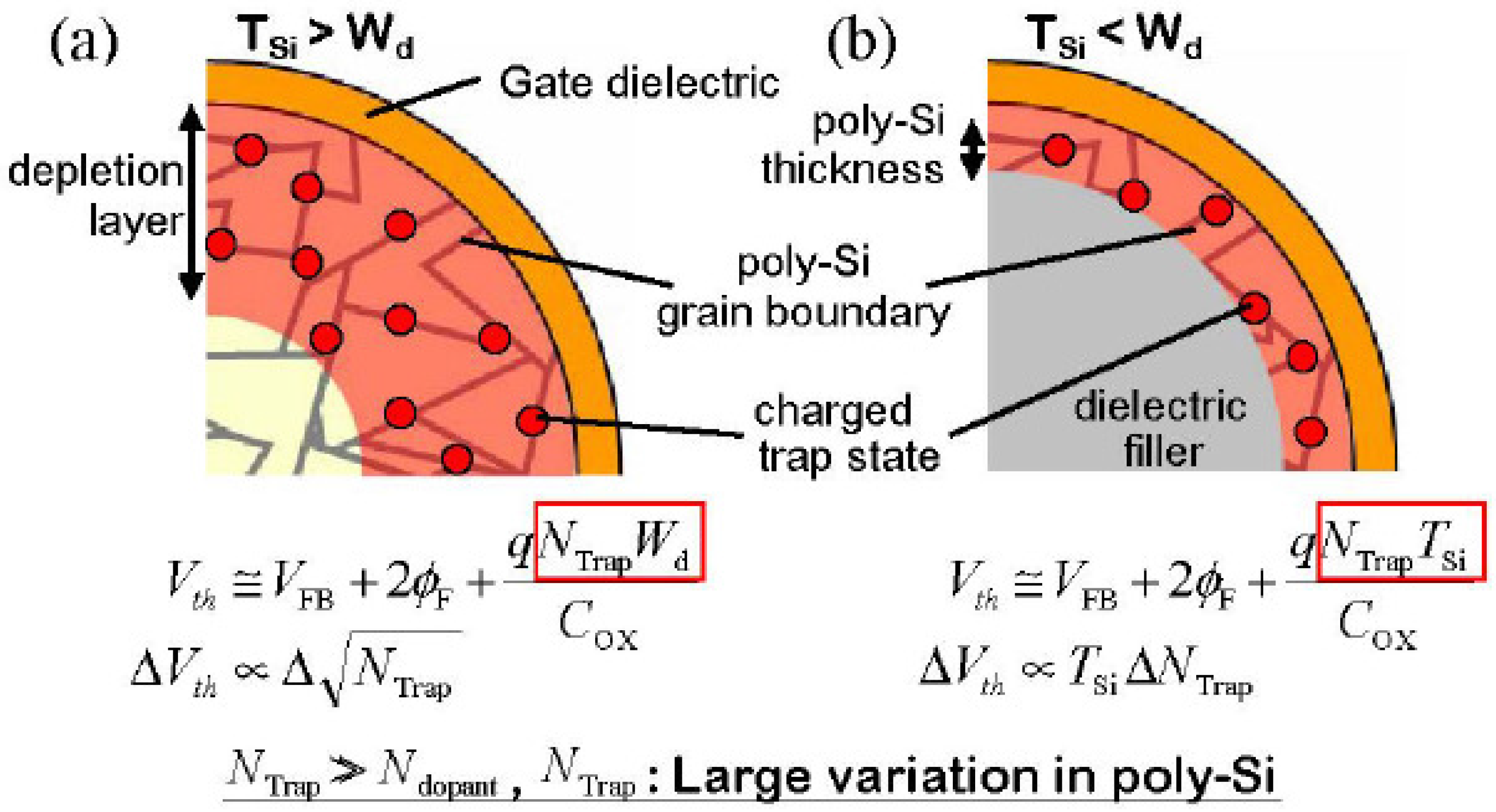
The single NAND Flash cell in BiCS design embodies the CT process option, whose structure is depicted in Figure 6. The transistor body is made of poly-silicon, since it is mandatory for achieving a good production yield that highly depends on the aspect ratio of the drilled pillars [17].
However, in the former configuration, there is an intrinsic difficulty in controlling the density of traps at grain boundaries, resulting in a significant variability of the sub-threshold current/voltage characteristics of the cells. To this extent, the body poly-silicon must be thinner than the depletion width, as shown in Figure 7 [8]. Due to the shape of the transistor, its body is informally known as the Macaronibody [8]. The CT process ends before the creation of the BLS, which is a standard transistor where the tunnel oxide and charge trapping material are replaced by poly-silicon, including only the field oxide. Similar considerations apply to SLS.
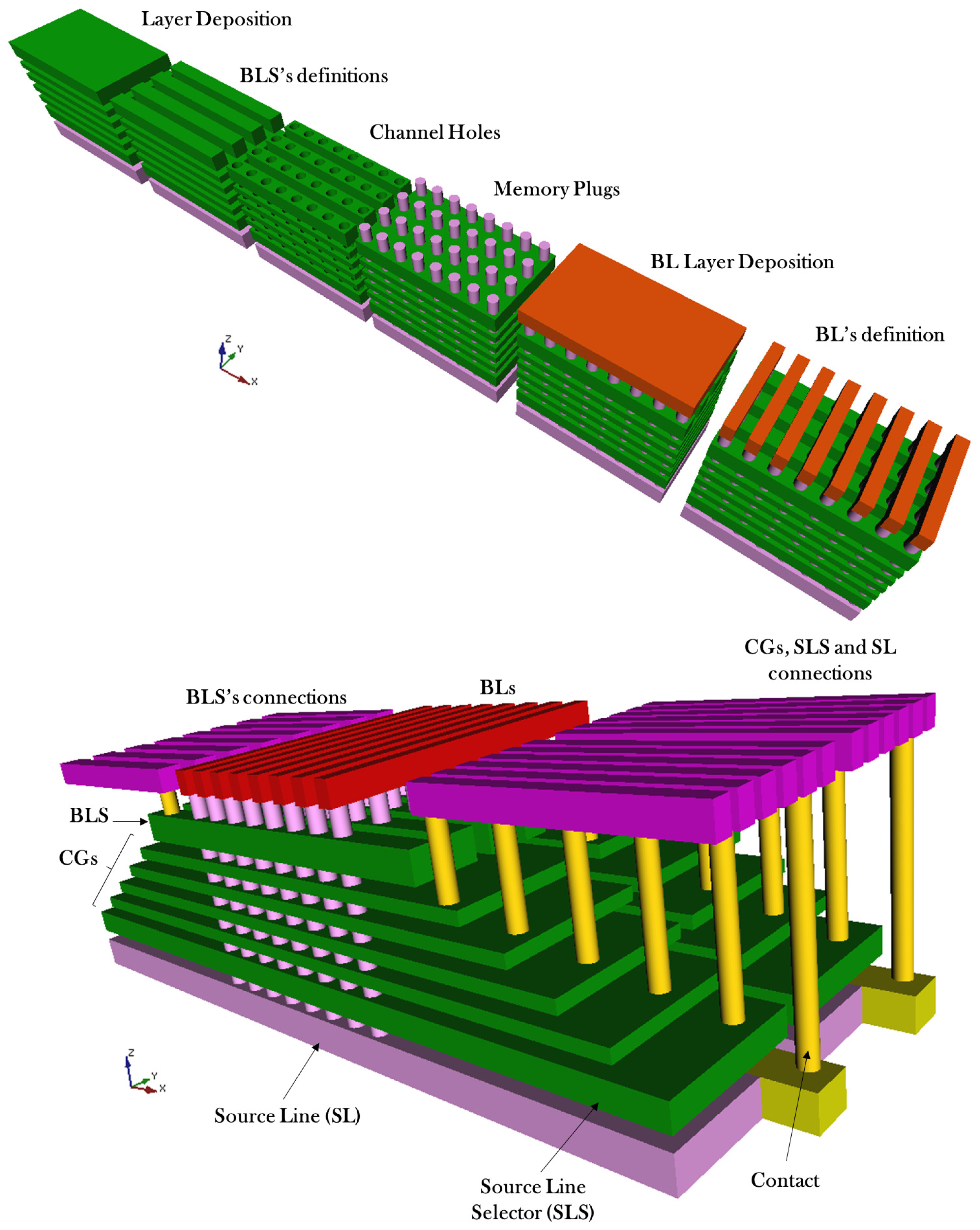
To give the reader an example of the manufacturing sequence of a BiCS 3D NAND Flash memory, we have provided a process step chain in Figure 8 [24]. Initially, there is the creation of the SLS, CG and BLS layer. Each single BLS stripe is then defined providing the structure to the drilling phase of the pillars that need to be filled by poly-silicon, CT material and field oxide. In the back-end of the process, the bitlines are defined and deposited. The memory cells are the intersection of the CG plates and the poly-silicon pillars. The edges of the CG plates create a double-sided staired structure [8,9,24,25]. CG, SLS and SL plates are contacted on the same side in the opposite direction of the BLS connections. The rectangles in orange are the metal interconnects.
Unfortunately, in this 3D NAND Flash architecture, we have more than a single NAND Flash page sharing the same CG plate, which amplifies disturbs in particular during the programming operation. The disturb minimization is achieved by etching the stacks at some defined points creating block slits.
4. P-BiCS Architecture
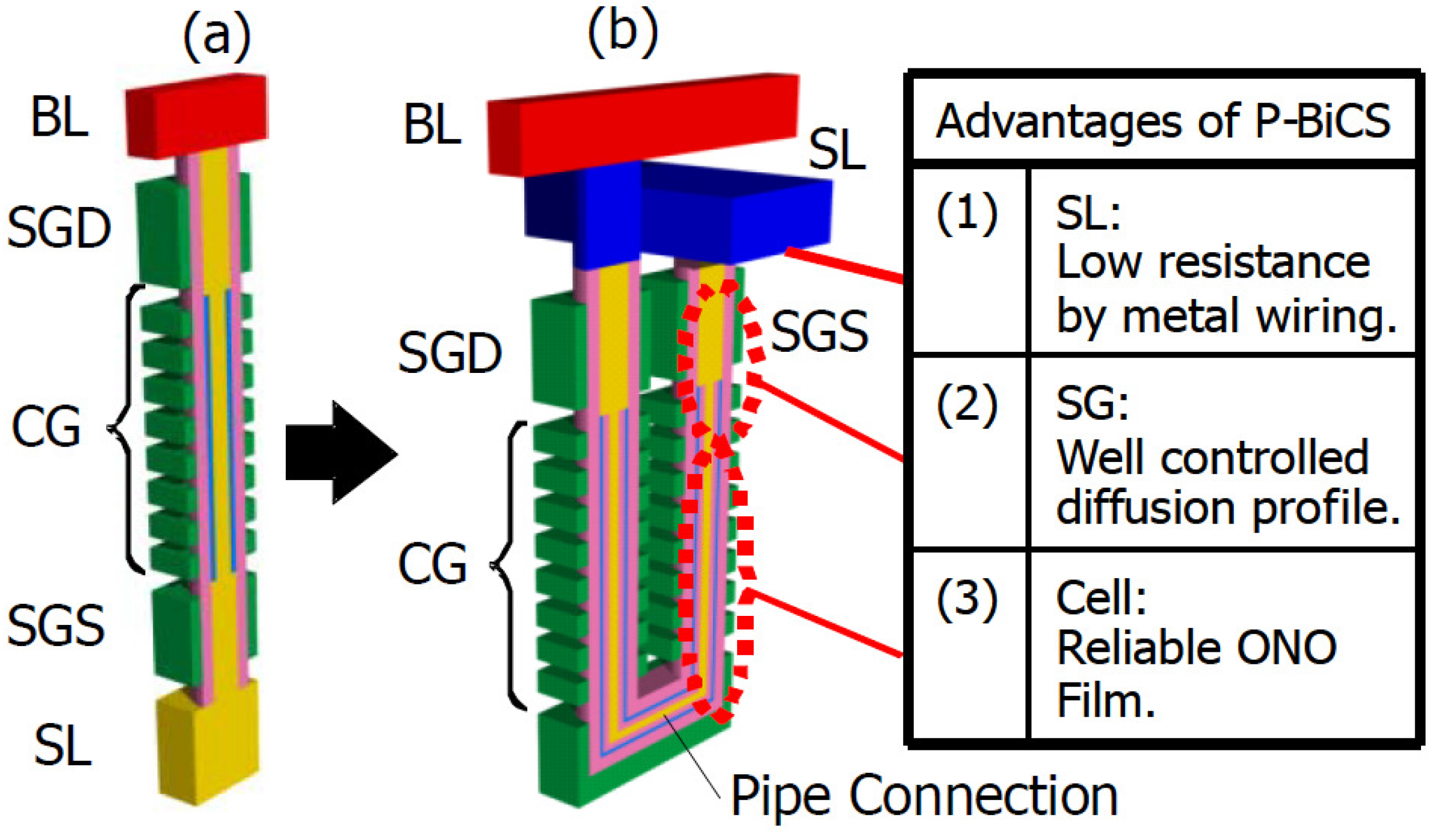
BiCS evidenced some critical issues such as poor reliability characteristics of the memory cells in terms of endurance and data retention, poor SLS performances (i.e., cut-off) and a high resistance of the SL, which limits the sensing performance [8,26]. To solve these issues, a pipe-shaped BiCS architecture has been developed, namely the P-BiCS. This integration approach adopts a U-shaped vertical NAND string, which seems to result in the following advantages:
- Since SL is located on the stack upper side, it reduces the parasitic resistance and the connection complexity to the metal levels.
- Placing SLS close to the BLS allows controlling accurately the current/voltage characteristics (i.e., especially the cut-off point) of both transistors, improving array functionality.
- Data retention and the threshold voltage margin between the programmed and erased states is enhanced since the fabrication process provides less tunnel oxide degradation.
The P-BiCS array starts from the structure depicted in Figure 9 [26]. In this architecture, there are two NAND Flash strings connected through a pipe connection in the bottom, thus forming a U-shaped string. One side is connected to the bitlines, whereas the other side is tied to SL. To improve the array integration efficiency, two strings share the same SL plate. By replicating the structure of Figure 9 multiple times, a larger array can be created, as shown in Figure 10.
As said in the introduction of this section, the SL plate is shared between NAND Flash strings that are in a mirrored position with respect to the U-shaped pillar. Such an interconnection scheme minimizes the parasitic resistance of the source connection and increases the sensing capabilities (i.e., better read characteristics of the memory.
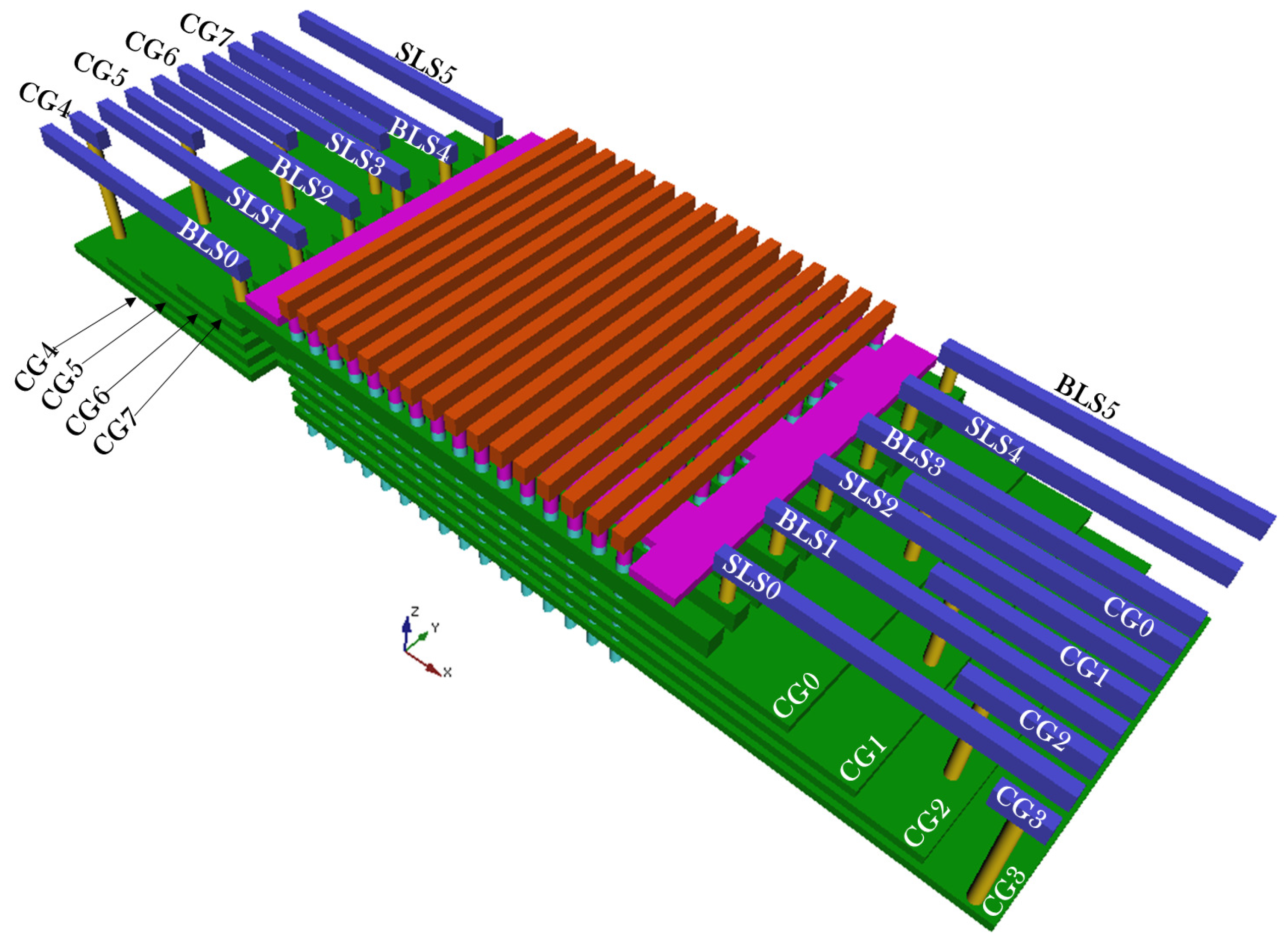
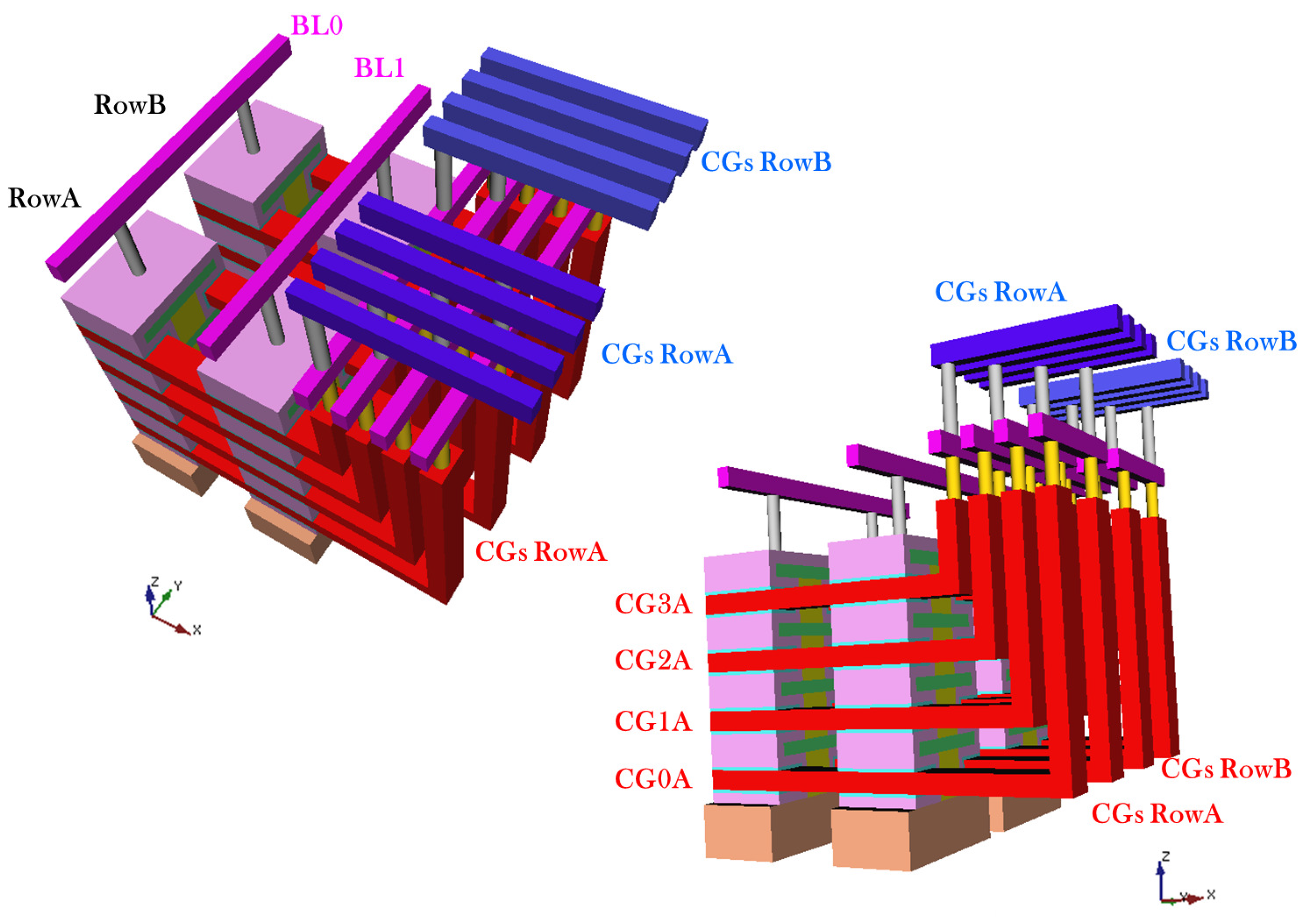
The larger part of the manufacturing process is devoted to designing the mandatory interconnections of the CG, BL, BLS, SL and SLS plates [11]. We have previously observed that in the BiCS architecture, each CG plate connects several adjacent NAND Flash strings to improve silicon area occupation and the integration efficiency. In the P-BiCS architecture, this solution is not affordable since two separate CGs of the same NAND Flash string belong to the same layer in the stack. To this extent, a branch-like CG structure is adopted, as shown in Figure 11. The figure shows a P-BiCS NAND Flash array with all of the interconnections in place by assuming for simplicity NAND Flash strings composed by eight cells.
The CGs fabrication process involves the creation of fork-shaped plates [11]. Each side of the fork controls the cells of two neighbor pages. Each CG plates pair is staggered; therefore, stacking four pairs of CGs as in Figure 11 yields NAND Flash strings composed of eight cells. By scaling the architecture, increasing the number of layers, it is possible to achieve larger string sizes. Figure 12 shows the detail of this fork-shaped structure.
A major difference between the BiCS and the P-BiCS architectures is the placement of the SL plate. In the former architecture, the SL plate is placed on the bottom of the stack [10], whereas in the latter, it is placed on top. A low resistance SL plate is required to additionally increase the noise immunity along with the sensing characteristics of the memory. For this purpose, P-BiCS adopts a top level SL connection, which is an additional layer usually referred to as top-level SL. Figure 13 shows a cross-section of this integration approach.
The final version of the P-BiCS 3D NAND Flash architecture with CG slits approaches for program/read disturb reduction is reported in Figure 14.
5. VRAT Architecture
A competitor architecture for the BiCS and P-BiCS concepts was introduced by Samsung. This new concept, called Vertical Recess Array Transistor (VRAT), was introduced back in 2008 [14], leading to all of the subsequent research activities on the well-known V-NAND product. The VRAT architecture concept is shown in Figure 15. A CT layer is used as a storage layer as in BiCS counterparts. The full integration flow for the VRAT arrays is called PIPE (Planarized Integration on the same PlanE), not to be confused with the pipe concept previously disclosed for P-BiCS. One of the VRAT goals was the development of a unique integration scheme for memory cells and array circuit interconnects, which is a requirement for manufacturing memory products in volume.
Let us take a closer look at the VRAT process technology. At the beginning, silicon nitride and silicon oxide films are deposited for multiple layers. The cell region is defined lithographically and then formed by a wet etching process. Once the cell’s stack is created, wordline electrodes are deposited, followed by an etch-back process, which separates the wordline layers by removing the electrode from the sidewall positions. Bitline and wordline contacts are then added to connect the peripheral circuitry to the final array (Figure 16). It is worth highlighting that, in this case, wordline fan-out is not a staircase, and this is one of the positive aspects of this architecture; indeed, by saving the lithography process steps for the staircase structural formation, this solution is potentially less expensive than others.
6. VSAT Architecture
The challenge of VRAT architecture lies in the creation of an undercut space for creating the CG electrodes and contacts, implying complex manufacturing. The Vertical Stacked Array Transistor (VSAT) architecture [15] is built with a reverse order compared to VRAT: the gate is integrated first, and the channel is obtained in the last process steps. The VSAT core is sketched in Figure 17. There are several poly-silicon layers and silicon nitride films: poly-silicon acts as the CG, whereas the silicon nitride is the dielectric material providing insulation. After layer patterning and etching, the active region is defined. A Chemical Mechanical Polishing (CMP) process is used to expose all of the CGs sharing the same plane, for easy access to gate electrodes. Cell’s layers (i.e., tunnel oxide, CT material and blocking oxide) are deposited above the active region. Finally, The vertical strings are isolated through an etching process.
One of the general challenges for all of the vertical-channel architectures is related to the placement of the SLS transistors. Since their location is at the bottom of the stack, it is difficult to achieve a standard transistor characteristic that differs from that of the single memory cells within the Flash strings constituting the array. The VSAT architecture addresses this challenge by moving the SLS outside the vertical string. The credit for this process option is a legacy from the 2D integration case. However, we must remind that all of the features of the PIPE process are unaltered, as clearly pointed out in Figure 18.
The main difference between VRAT and VSAT in terms of achievable bit density is related to the connection of the so-called “twin” cells. In the VRAT, the cells are split into two parts that are integrated in parallel, whereas in the VSAT, the twin cells are in series, with a consequent burden on the integration storage density. To this extent, Macronix proposed, back in 2015, an improved architecture called Asymmetrical VSAT (A-VSAT) that includes a supplementary wordline cut process [27].
7. TCAT Architecture
In 2009, Samsung proposed an alternative to the BiCS architecture, namely the Terabit Cell Array Transistor (TCAT) [16]. A view of the overall array organization is presented in Figure 19.
From the electrical standpoint, the TCAT circuit scheme is the same as the BiCS scheme already presented in this paper, with a difference in the source plate. In TCAT, the SL lines are made by the -silicon diffusion shorted together to a common source line that is placed outside the cells array. Two metallization levels are deposited to decode the BLSs and CGs/SLS elements, respectively. To understand the peculiarities of the TCAT architecture, let us assume an example array with the configuration depicted in Figure 20. In the figure, we show two NAND Flash blocks each one constituted by seven wordlines and six CG layers. All of the wordlines are connected to the Metal1 level, so that with this metallization, it is possible to decode the NAND Flash strings, whereas with the additional Metal2 level, it is possible to decode the wordline. By comparing TCAT with BiCS, it is possible to observe that the blocks slit is visible as a cut in the bitline layer.
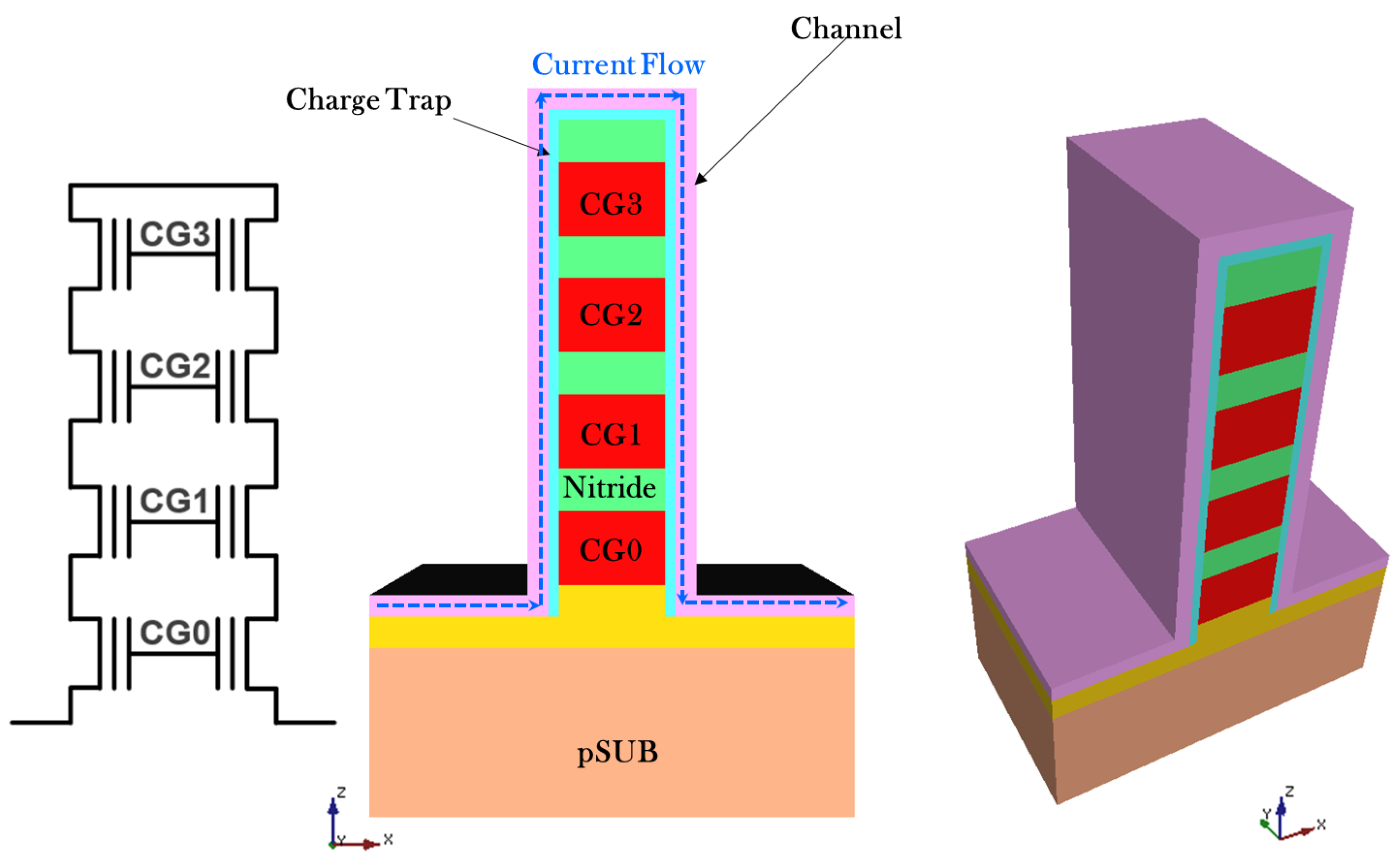
Besides the difference in architectural elements of TCAT and BiCS structures, there are some significant technology replacements that should be investigated in the former architecture. TCAT uses an integration technique called gate-replacement [16], which is constituted by depositing the gate layer only in the last step of the stack manufacturing process. The BiCS architecture, on the contrary, exploits a gate-first approach. The former gate creation technology deposits several layers of silicon dioxide and sacrificial silicon nitride layers that are etched between each row of pillars. Dielectrics and metal gates are then deposited in the conventional order by filling the wordline space with tungsten. A final etching process will separate the CGs. The created memory cell is a Silicon-Oxide-Nitride-Oxide-Silicon (SONOS)-type, which provides advantages in terms of erase speed, data retention and threshold voltage distribution margins. Further, having a metal gate allows reducing the parasitic resistance of the wordline contact, thus meaning faster operations.
Operational differences between TCAT and BiCS are also evidenced in terms of bulk erase. In TCAT, the vertical pillar is connected to a p-type silicon substrate rather than a -diffusion. Near each NAND Flash string, there is a diffusion region to drain the cell’s current. During the erase operation, holes are provided by the silicon substrate without requiring the Gate-Induced Drain Leakage (GIDL) phenomenon generation at the SLS-side, which is a concern for BiCS.
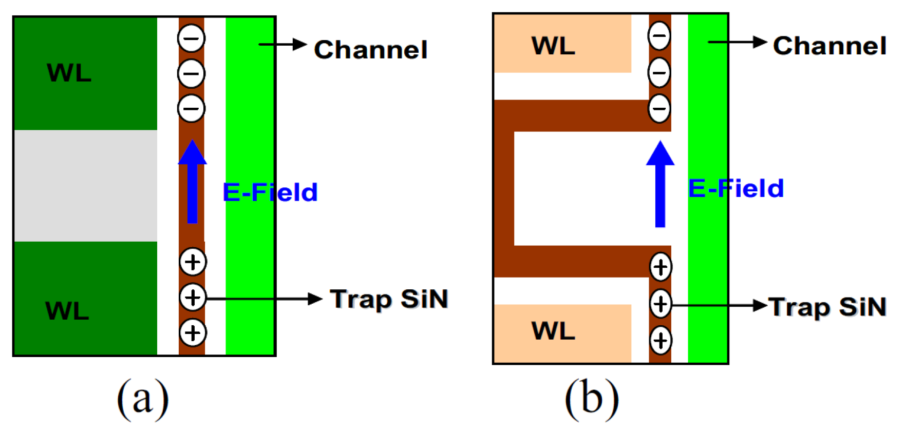
Finally, the last comparison is evidenced in Figure 21. The gate-last process of TCAT cells results in a biconcave memory cell shape, which reduces the charge spreading issue. Indeed, in BiCS architectures, since the trapping layer is electrically connected in a continuous way along the channel side, there is a significant charge spreading path resulting in potential reliability issues [28].
8. V-NAND Architecture
The V-NAND architecture proposed by Samsung in 2013 [29] is actually the first 3D NAND Flash concept brought to mass production, stemming from the initial work made on the development of the TCAT architecture. The official introduction to the market of the V-NAND dates back to 2014 [30,31], when a 128-Gb 2-bit/cell product embodied a damascened CT cell option (i.e., a SONOS memory cell) and 24 layers (see Figure 22).
In this architecture, two dummy wordlines (i.e., dummy CG plates) are integrated close to the BLSs and SLSs. These additional structures are needed to shield the edge wordlines from the program disturb. Indeed, during program operation, high channel boosting potential may generate hot carriers at the string edges due to the high lateral electric field. This translates into program disturb and corruption of the threshold voltage distributions [32,33].
The first V-NAND generation exploits a special integration scheme for the pillars, better known as staggered pillars. Even and odd pillars are staggered without changing the central distance between adjacent structures. In this case, each bitline has to fit in a single pillar pitch [31].
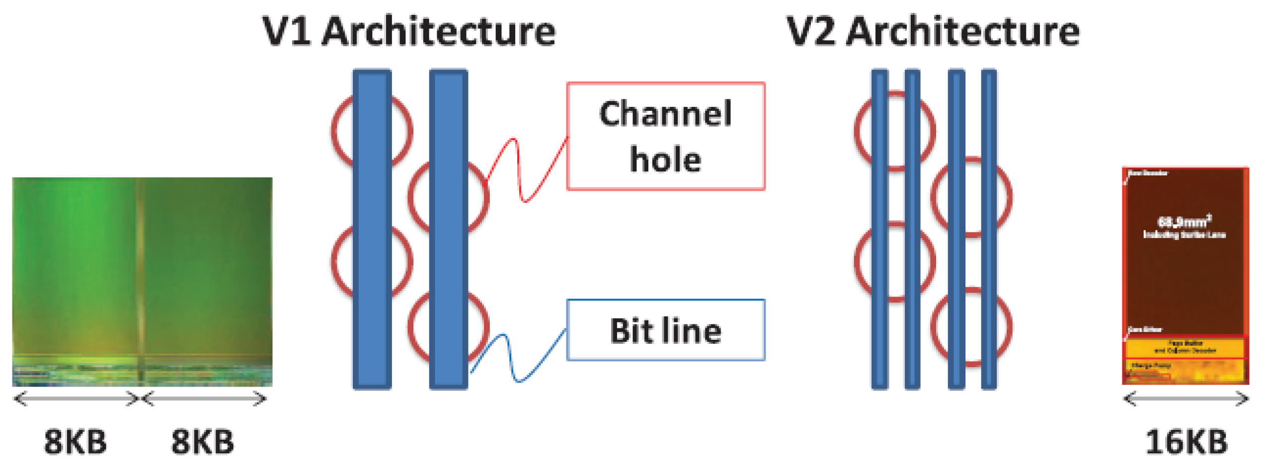
The second V-NAND generation has been introduced in 2015 by increasing the storage bit density from two bits/cell to three bits/cell [12]. Comparing with the previous generation, there were not many macroscopic changes in the memory cell structure, although the number of layers switched from 24 to 32. The bitlines layout is different as sketched in Figure 23. In this case, two bitlines are arranged in a single pillar pitch [12]. BL density is doubled (i.e., the NAND Flash page size step from 8 kB to 16 kB), but the number of contacts to the SL plate is halved. However, the overall number of pillars is the same as the first generation V-NAND. Another highlight of the second generation V-NAND is the so-called single-sequence programming.In this improved algorithm, the V-NAND asks for 3 NAND Flash pages at the start of the programming, and it writes the pages at once, turning into faster operations and lower power consumption.
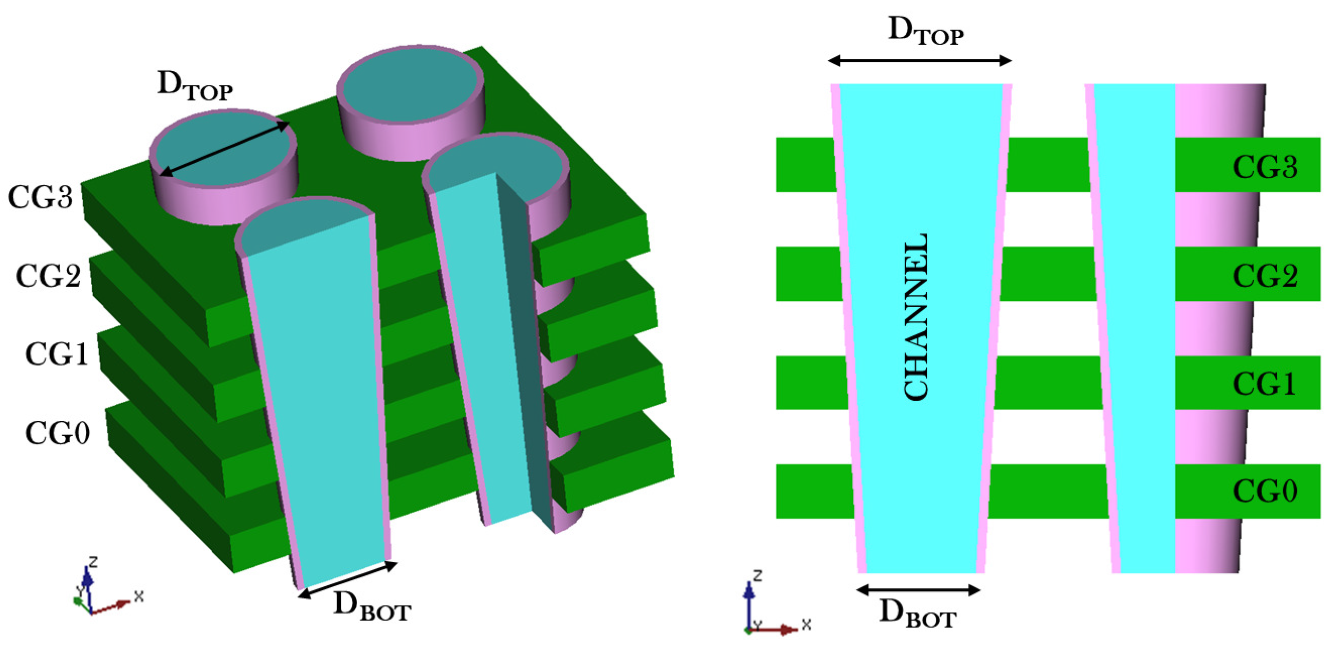
The third generation of V-NAND architecture became public in 2016 [13]. It is still a three bits/cell architecture, but this time, it is a 256-Gb product based on a stack of 48 layers. When the number of layers increases, the etching technology becomes a serious issue due to the aspect ratio of the pillar (see Figure 24). Therefore, the only solution is to reduce the layers’ thickness with severe drawbacks on the wordline features like the parasitic resistance and capacitance. Moreover, as the parasitic resistance increases, the channel hole size fluctuations are even more important in the charge flow control across the wordline. An adaptive program pulse scheme per wordline is therefore applied to increase the overall reliability of the memory. The algorithm basically varies the program pulse duration according to the target wordline characteristics.
The general scaling trend for every 3D NAND Flash technology is to increase the number of integrated layers. However, this has a negative impact on the geometry of the pillar (i.e., the aspect ratio) since it becomes longer. The compensation of such a layout degradation is visible in the fourth V-NAND generation [35], which exploits a 64-layer stack. In this architecture variant, the layer thickness and the intra-layer spacing shrinked, with adverse effects on the cell’s reliability and timings. Improved programming algorithms and ad hoc circuits can be used to reduce the parasitic wordline capacitance effects derived by layer scaling [35].
9. Conclusions
In this work, we disclosed many 3D NAND Flash architectures, including some of the concepts that reached mass production in recent years. Most NAND Flash vendors are calling for more layers with multi-bits per cell storage paradigms, including four bits/cell. In the future, we will experience many innovations: scientists and engineers are urged to give their best effort to fuel this evolution.
Acknowledgments
This work has been partially supported by the Università degli Studi di Ferrara through the initiative Bando per il finanziamento della ricerca scientifica “Fondo per l’Incentivazione alla Ricerca” (FIR)—2016.
Conflicts of Interest
The authors declare no conflict of interest.
References
- Micheloni, R.; Crippa, L.; Marelli, A. (Eds.) Inside NAND Flash Memories; Springer: Dordrecht, The Netherlands, 2010. [Google Scholar]
- Mizuno, T.; Okumtura, J.; Toriumi, A. Experimental study of threshold voltage fluctuation due to statistical variation of channel dopant number in MOSFET’s. IEEE Trans. Electron Devices 1994, 41, 2216–2221. [Google Scholar] [CrossRef]
- Monzio Compagnoni, C.; Spinelli, A.; Beltrami, S.; Bonanomi, M.; Visconti, A. Cycling Effect on the Random Telegraph Noise Instabilities of NOR and NAND Flash Arrays. IEEE Electron Device Lett. 2008, 29, 941–943. [Google Scholar] [CrossRef]
- Monzio Compagnoni, C.; Spinelli, A.S.; Gusmeroli, R.; Beltrami, S.; Ghetti, A.; Visconti, A. Ultimate Accuracy for the NAND Flash Program Algorithm Due to the Electron Injection Statistics. IEEE Trans. Electron Devices 2008, 55, 2695–2702. [Google Scholar] [CrossRef]
- Whang, S.; Lee, K.; Shin, D.; Kim, B.; Kim, M.; Bin, J.; Han, J.; Kim, S.; Lee, B.; Jung, Y.; et al. Novel 3-dimensional Dual Control-gate with Surrounding Floating-gate (DC-SF) NAND flash cell for 1 Tb file storage application. In Proceedings of the 2010 IEEE International Conference on Electron Devices Meeting (IEDM), San Francisco, CA, USA, 6–8 December 2010; pp. 29.7.1–29.7.4. [Google Scholar]
- Tanaka, T.; Helm, M.; Vali, T.; Ghodsi, R.; Kawai, K.; Park, J.K.; Yamada, S.; Pan, F.; Einaga, Y.; Ghalam, A.; et al. A 768 Gb 3b/cell 3D-floating-gate NAND flash memory. In Proceedings of the IEEE International Solid-State Circuits Conference, San Francisco, CA, USA, 31 January–4 February 2016; pp. 142–144. [Google Scholar]
- Park, K.T.; Kang, M.; Hwang, S.; Kim, D.; Cho, H.; Jeong, Y.; Seo, Y.I.; Jang, J.; Kim, H.S.; Lee, Y.T.; et al. A Fully Performance Compatible 45 nm 4-Gigabit Three Dimensional Double-Stacked Multi-Level NAND Flash Memory with Shared Bit-Line Structure. IEEE J. Solid State Circuit 2009, 44, 208–216. [Google Scholar] [CrossRef]
- Fukuzumi, Y.; Katsumata, R.; Kito, M.; Kido, M.; Sato, M.; Tanaka, H.; Nagata, Y.; Matsuoka, Y.; Iwata, Y.; Aochi, H.; et al. Optimal Integration and Characteristics of Vertical Array Devices for Ultra-High Density, Bit-Cost Scalable Flash Memory. In Proceedings of the IEEE International Conference on Electron Devices Meeting (IEDM), Washington, DC, USA, 10–12 December 2007; pp. 449–452. [Google Scholar]
- Tanaka, H.; Kido, M.; Yahashi, K.; Oomura, M.; Katsumata, R.; Kito, M.; Fukuzumi, Y.; Sato, M.; Nagata, Y.; Matsuoka, Y.; et al. Bit Cost Scalable Technology with Punch and Plug Process for Ultra High Density Flash Memory. In Proceedings of the 2007 IEEE Symposium on VLSI Technology, Kyoto, Japan, 12–14 June 2007; pp. 14–15. [Google Scholar]
- Ishiduki, M.; Fukuzumi, Y.; Katsumata, R.; Kito, M.; Kido, M.; Tanaka, H.; Komori, Y.; Nagata, Y.; Fujiwara, T.; Maeda, T.; et al. Optimal device structure for Pipe-shaped BiCS Flash memory for ultra high density storage device with excellent performance and reliability. In Proceedings of the 2009 IEEE International Conference on Electron Devices Meeting (IEDM), Baltimore, MD, USA, 7–9 December 2009; pp. 1–4. [Google Scholar]
- Katsumata, R.; Kito, M.; Fukuzumi, Y.; Kido, M.; Tanaka, H.; Komori, Y.; Ishiduki, M.; Matsunami, J.; Fujiwara, T.; Nagata, Y.; et al. Pipe-shaped BiCS flash memory with 16 stacked layers and multi-level-cell operation for ultra high density storage devices. In Proceedings of the 2009 Symposium on VLSI Technology, Honolulu, HI, USA, 16–18 June 2009; pp. 136–137. [Google Scholar]
- Im, J.W.; Jeong, W.P.; Kim, D.H.; Nam, S.W.; Shim, D.K.; Choi, M.H.; Yoon, H.J.; Kim, D.H.; Kim, Y.S.; Park, H.W.; et al. A 128 Gb 3b/cell V-NAND flash memory with 1 Gb/s I/O rate. In Proceedings of the IEEE International Solid-State Circuits Conference, San Francisco, CA, USA, 22–26 February 2015; pp. 1–3. [Google Scholar]
- Kang, D.; Jeong, W.; Kim, C.; Kim, D.H.; Cho, Y.S.; Kang, K.T.; Ryu, J.; Kang, K.M.; Lee, S.; Kim, W.; et al. 256 Gb 3b/cell V-NAND flash memory with 48 stacked WL layers. In Proceedings of the IEEE International Solid-State Circuits Conference, San Francisco, CA, USA, 31 January–4 February 2016; pp. 130–131. [Google Scholar]
- Kim, J.; Hong, A.J.; Ogawa, M.; Ma, S.; Song, E.B.; Lin, Y.S.; Han, J.; Chung, U.I.; Wang, K.L. Novel 3-D structure for ultra high density flash memory with VRAT (Vertical-Recess-Array-Transistor) and PIPE (Planarized Integration on the same PlanE). In Proceedings of the 2008 Symposium on VLSI Technology, Honolulu, HI, USA, 17–19 June 2008; pp. 122–123. [Google Scholar]
- Kim, J.; Hong, A.J.; Kim, S.M.; Song, E.B.; Park, J.H.; Han, J.; Choi, S.; Jang, D.; Moon, J.T.; Wang, K.L. Novel Vertical-Stacked-Array-Transistor (VSAT) for ultra-high-density and cost-effective NAND Flash memory devices and SSD (Solid State Drive). In Proceedings of the 2009 Symposium on VLSI Technology, Honolulu, HI, USA, 16–18 June 2009; pp. 186–187. [Google Scholar]
- Jang, J.; Kim, H.S.; Cho, W.; Cho, H.; Kim, J.; Shim, S.I.; Jang, Y.; Jeong, J.H.; Son, B.K.; Kim, D.W.; et al. Vertical cell array using TCAT(Terabit Cell Array Transistor) technology for ultra high density NAND flash memory. In Proceedings of the 2009 Symposium on VLSI Technology, Honolulu, HI, USA, 16–18 June 2009; pp. 192–193. [Google Scholar]
- Micheloni, R. (Ed.) 3D Flash Memories; Springer: Dordrecht, The Netherlands, 2016. [Google Scholar]
- Lai, E.K.; Lue, H.T.; Hsiao, Y.H.; Hsieh, J.Y.; Lu, C.P.; Wang, S.Y.; Yang, L.W.; Yang, T.; Chen, K.C.; Gong, J.; et al. A Multi-Layer Stackable Thin-Film Transistor (TFT) NAND-Type Flash Memory. In Proceedings of the 2006 International Electron Devices Meeting (IEDM), San Francisco, CA, USA, 11–13 December 2006; pp. 1–4. [Google Scholar]
- Jung, S.M.; Jang, J.; Cho, W.; Cho, H.; Jeong, J.; Chang, Y.; Kim, J.; Rah, Y.; Son, Y.; Park, J.; et al. Three Dimensionally Stacked NAND Flash Memory Technology Using Stacking Single Crystal Si Layers on ILD and TANOS Structure for Beyond 30 nm Node. In Proceedings of the 2006 International Electron Devices Meeting (IEDM), San Francisco, CA, USA, 11–13 December 2006; pp. 1–4. [Google Scholar]
- Suh, K.D.; Suh, B.H.; Um, Y.H.; Kim, J.K.; Choi, Y.J.; Koh, Y.N.; Lee, S.S.; Kwon, S.C.; Choi, B.S.; Yum, J.S.; et al. A 3.3 V 32 Mb NAND Flash Memory with Incremental Step Pulse Programming Scheme. In Proceedings of the IEEE International Solid-State Circuits Conference, San Francisco, CA, USA, 15–17 February 1995; pp. 128–129. [Google Scholar]
- Aochi, H. BiCS Flash as a Future 3D Non-Volatile Memory Technology for Ultra High Density Storage Devices. In Proceedings of the IEEE International Memory Workshop, Monterey, CA, USA, 10–14 May 2009; pp. 1–2. [Google Scholar]
- Nishi, Y. (Ed.) Advances in Non-Volatile Memory and Storage Technology; Woodhead Publishing: Cambridge, UK, 2014. [Google Scholar]
- Yanagihara, Y.; Miyaji, K.; Takeuchi, K. Control Gate Length, Spacing and Stacked Layer Number Design for 3D-Stackable NAND Flash Memory. In Proceedings of the IEEE International Memory Workshop, Milan, Italy, 20–23 May 2012; pp. 1–4. [Google Scholar]
- Nitayama, A.; Aochi, H. Bit Cost Scalable (BiCS) flash technology for future ultra high density storage devices. In Proceedings of the VLSI Technology, Systems, and Applications, Hsin Chu, Taiwan, 26–28 April 2010; pp. 130–131. [Google Scholar]
- Komori, Y.; Kido, M.; Kito, M.; Katsumata, R.; Fukuzumi, Y.; Tanaka, H.; Nagata, Y.; Ishiduki, M.; Aochi, H.; Nitayama, A. Disturbless flash memory due to high boost efficiency on BiCS structure and optimal memory film stack for ultra high density storage device. In Proceedings of the IEEE International Electron Devices Meeting (IEDM), San Francisco, CA, USA, 15–17 December 2008; pp. 1–4. [Google Scholar]
- Maeda, T.; Itagaki, K.; Hishida, T.; Katsumata, R.; Kito, M.; Fukuzumi, Y.; Kido, M.; Tanaka, H.; Komori, Y.; Ishiduki, M.; et al. Multi-stacked 1 G cell/layer Pipe-shaped BiCS flash memory. In Proceedings of the 2009 Symposium on VLSI Circuits, Kyoto, Japan, 16–18 June 2009; pp. 22–23. [Google Scholar]
- Hsiao, Y.H.; Lue, H.T.; Chen, W.C.; Tsui, B.Y.; Hsieh, K.Y.; Lu, C.Y. Ultra-High Bit Density 3D NAND Flash-Featuring-Assisted Gate Operation. IEEE Electron Device Lett. 2015, 36, 1015–1017. [Google Scholar] [CrossRef]
- Cho, W.S.; Shim, S.I.; Jang, J.; Cho, H.S.; You, B.K.; Son, B.K.; Kim, K.H.; Shim, J.J.; Park, C.M.; Lim, J.S.; et al. Highly reliable vertical NAND technology with biconcave shaped storage layer and leakage controllable offset structure. In Proceedings of the 2010 Symposium on VLSI Technology, Honolulu, HI, USA, 15–17 June 2010; pp. 173–174. [Google Scholar]
- Elliott, J.; Jung, E.S. Ushering in the 3D Memory Era with V-NAND. In Proceedings of the Flash Memory Summit, Santa Clara, CA, USA, 13–15 August 2013. [Google Scholar]
- Park, K.T.; Byeon, D.S.; Kim, D.H. A world’s first product of three-dimensional vertical NAND Flash memory and beyond. In Proceedings of the 2014 14th Annual Non-Volatile Memory Technology Symposium (NVMTS), Jeju Island, Korea, 27–29 October 2014; pp. 1–5. [Google Scholar]
- Park, K.T.; Nam, S.; Kim, D.; Kwak, P.; Lee, D.; Choi, Y.H.; Choi, M.H.; Kwak, D.H.; Kim, D.H.; Kim, M.S.; et al. Three-Dimensional 128 Gb MLC Vertical nand Flash Memory With 24-WL Stacked Layers and 50 MB/s High-Speed Programming. IEEE J. Solid State Circuit 2015, 50, 204–213. [Google Scholar] [CrossRef]
- Choi, E.S.; Park, S.K. Device considerations for high density and highly reliable 3D NAND flash cell in near future. In Proceedings of the 2012 IEEE International Electron Devices Meeting (IEDM), San Francisco, CA, USA, 10–13 December 2012; pp. 9.4.1–9.4.4. [Google Scholar]
- Shim, K.S.; Choi, E.S.; Jung, S.W.; Kim, S.H.; Yoo, H.S.; Jeon, K.S.; Joo, H.S.; Oh, J.S.; Jang, Y.S.; Park, K.J.; et al. Inherent Issues and Challenges of Program Disturbance of 3D NAND Flash Cell. In Proceedings of the 2012 4th IEEE International Memory Workshop, Milan, Italy, 20–23 May 2012; pp. 1–4. [Google Scholar]
- Jeong, W.; Im, J.W.; Kim, D.H.; Nam, S.W.; Shim, D.K.; Choi, M.H.; Yoon, H.J.; Kim, D.H.; Kim, Y.S.; Park, H.W.; et al. A 128 Gb 3b/cell V-NAND Flash Memory with 1 Gb/s I/O Rate. IEEE J. Solid State Circuit 2016, 51, 204–212. [Google Scholar]
- Kim, C.; Cho, J.H.; Jeong, W.; Park, I.H.; Park, H.W.; Kim, D.H.; Kang, D.; Lee, S.; Lee, J.S.; Kim, W.; et al. A 512 Gb 3b/cell 64-stacked WL 3D V-NAND flash memory. In Proceedings of the IEEE International Solid-State Circuits Conference, San Francisco, CA, USA, 5–9 February 2017; pp. 202–203. [Google Scholar]
Figure 1.
Bird’s-eye view of a two-layer 3D stacked NAND Flash. SLS, source line selector; BLS, bitline selector.
Figure 1.
Bird’s-eye view of a two-layer 3D stacked NAND Flash. SLS, source line selector; BLS, bitline selector.

Figure 2.
(Left) Cross-sectional view and (Right) top layout view of the 3D stacked NAND string. GSL and SSL are the BLS and SLS, respectively. CSL is the common source line. Reproduced with permission from [7]. © 2009 IEEE.
Figure 2.
(Left) Cross-sectional view and (Right) top layout view of the 3D stacked NAND string. GSL and SSL are the BLS and SLS, respectively. CSL is the common source line. Reproduced with permission from [7]. © 2009 IEEE.
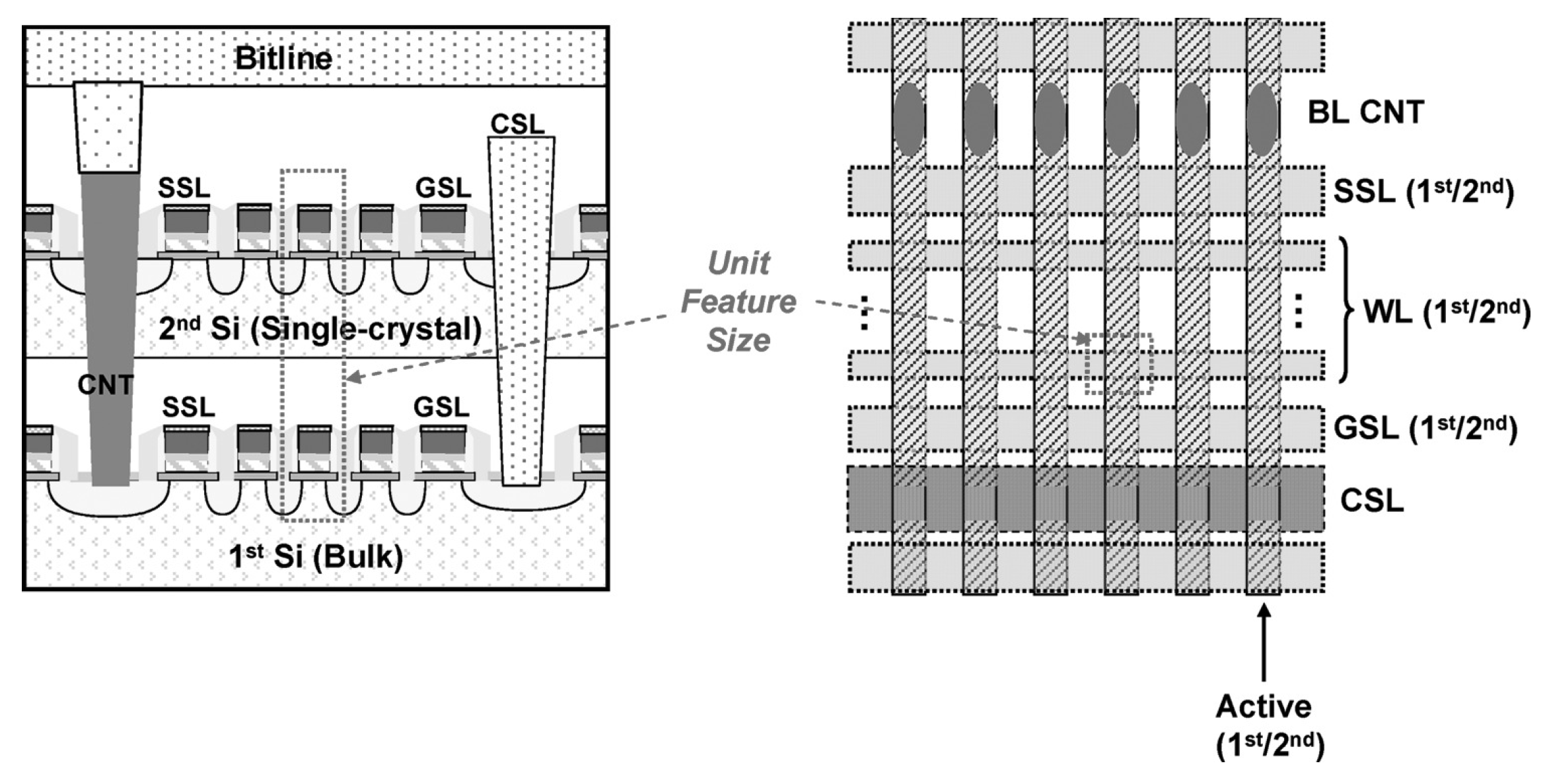
Figure 3.
Architectural scheme of a two-layer 3D stacked NAND Flash. MAT1 and MAT2 represent the two different layers.
Figure 3.
Architectural scheme of a two-layer 3D stacked NAND Flash. MAT1 and MAT2 represent the two different layers.

Figure 4.
Typical memory cell threshold voltage distribution of 3D stacked NAND Flash. Reproduced with permission from [7]. © 2009 IEEE.
Figure 4.
Typical memory cell threshold voltage distribution of 3D stacked NAND Flash. Reproduced with permission from [7]. © 2009 IEEE.

Figure 5.
(a) Bird’s-eye view of BiCS Flash memory; (b) top-down view of BiCS Flash memory array; (c) enlarged view of the memory string; (d) cross-sectional SEM image of the BiCS Flash memory array. Upper SG and lower SG are the BLS and SLS, respectively. Reproduced with permission from [8]. © 2007 IEEE.

Figure 6.
BiCS memory cells structure with highlighted layers: tunnel oxide, field oxide and charge trapping material, respectively.
Figure 6.
BiCS memory cells structure with highlighted layers: tunnel oxide, field oxide and charge trapping material, respectively.

Figure 7.
Schematics of dependence on trap density at poly-silicon grain boundaries when (a) and (b) . Reproduced with permission from [8]. © 2007 IEEE.
Figure 7.
Schematics of dependence on trap density at poly-silicon grain boundaries when (a) and (b) . Reproduced with permission from [8]. © 2007 IEEE.

Figure 8.
BiCS fabrication sequence: (top) plates’ creation, BLS definition, pillars’ drilling, memory cell stack plugs and BL deposition and definition; (bottom) adjacent blocks of a BiCS memory from a bird’s-eye view.
Figure 8.
BiCS fabrication sequence: (top) plates’ creation, BLS definition, pillars’ drilling, memory cell stack plugs and BL deposition and definition; (bottom) adjacent blocks of a BiCS memory from a bird’s-eye view.

Figure 9.
Schematics of (a) straight-shaped BiCS and (b) Pipe-shaped BiCS (P-BiCS). SGD and SGS are the BLS and SLS, respectively. The ONO material used in the cells is a stack silcon dioxide-silicon nitride-silicon dioxide. Reproduced with permission from [10]. © 2009 IEEE.
Figure 9.
Schematics of (a) straight-shaped BiCS and (b) Pipe-shaped BiCS (P-BiCS). SGD and SGS are the BLS and SLS, respectively. The ONO material used in the cells is a stack silcon dioxide-silicon nitride-silicon dioxide. Reproduced with permission from [10]. © 2009 IEEE.

Figure 10.
P-BiCS 3D NAND Flash array.
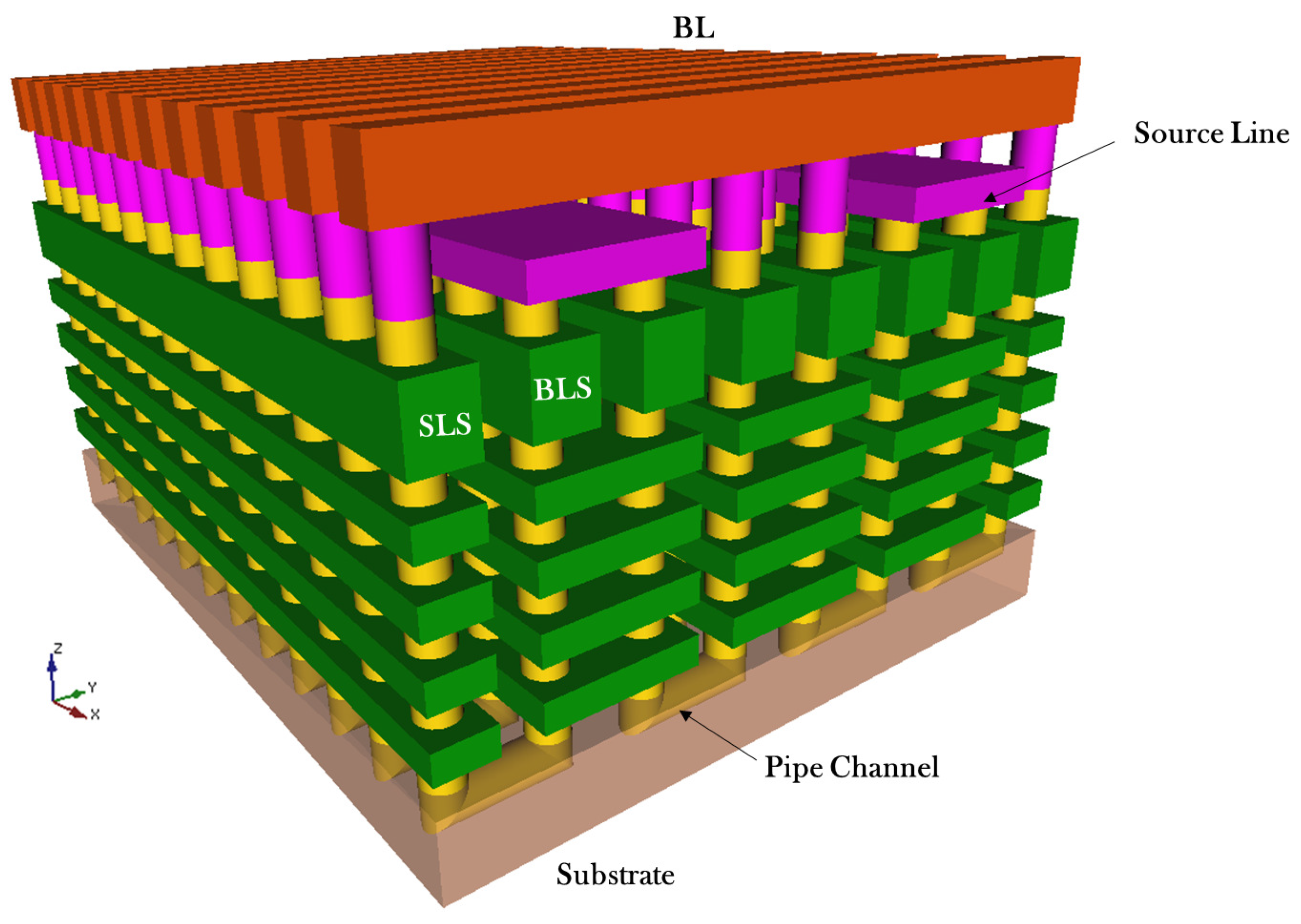
Figure 11.
P-BiCS 3D NAND Flash array with branched CG structures highlighted in a bird’s-eye view.

Figure 12.
Bird’s-eye view of a P-BiCS 3D NAND Flash array showing the fork-shaped structure.

Figure 13.
Cross-section of the P-BiCS array evidencing the top-level SL.
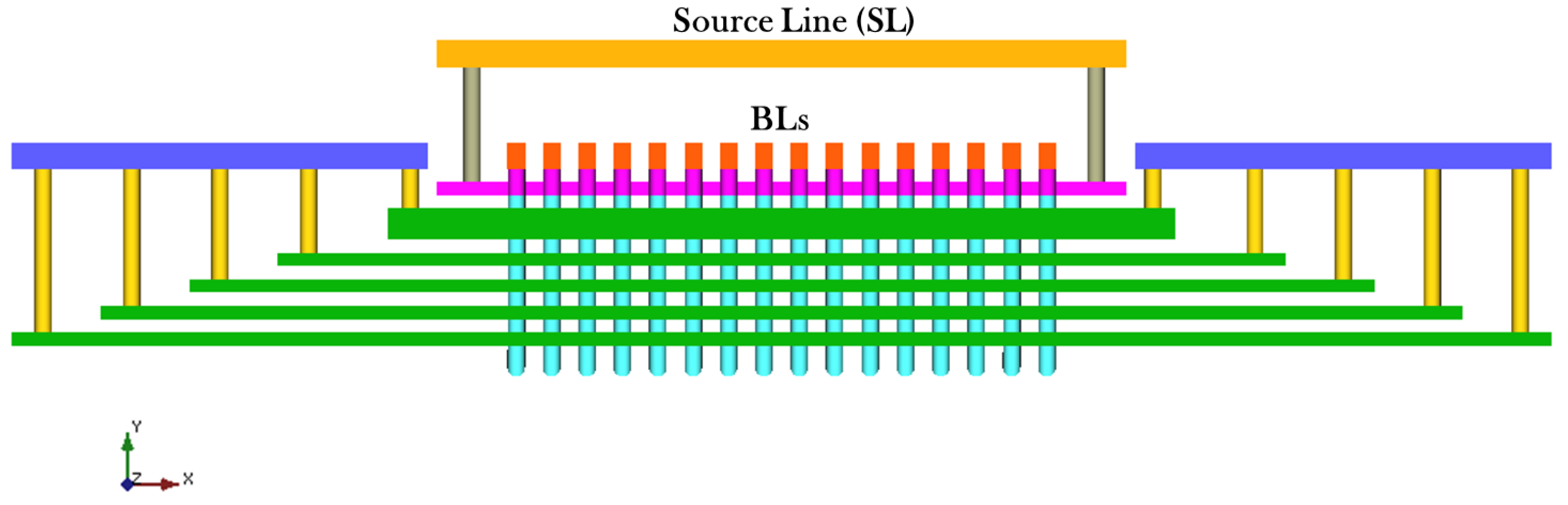
Figure 14.
Final realization of a P-BiCS 3D NAND Flash array with CG block slits evidenced.

Figure 15.
VRAT NAND Flash string.
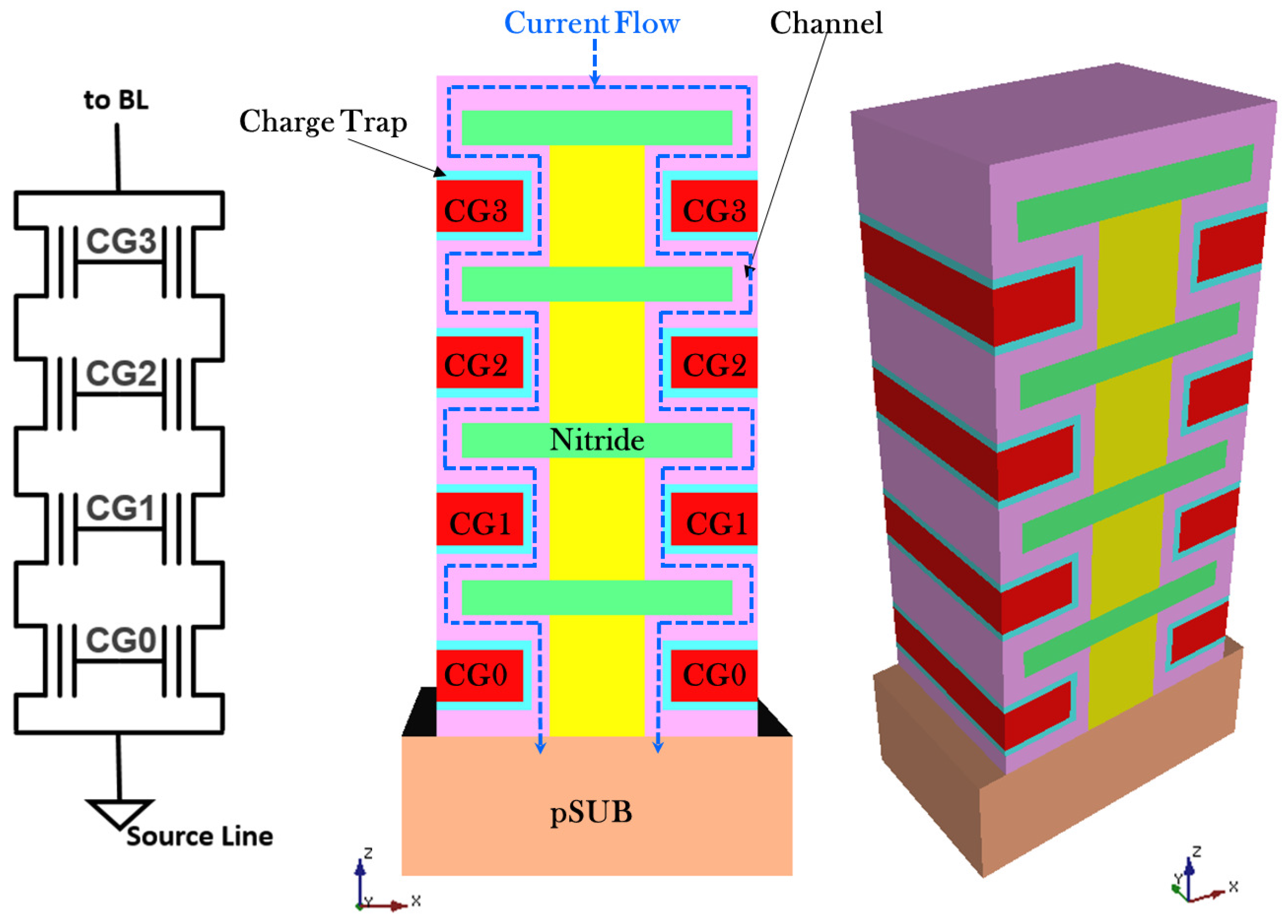
Figure 16.
VRAT array with bitline and wordline connections.

Figure 17.
VSAT basic building blocks.

Figure 18.
VSAT typical fan-out.

Figure 19.
Bird’s-eye view of a Terabit Cell Array Transistor (TCAT) architecture.
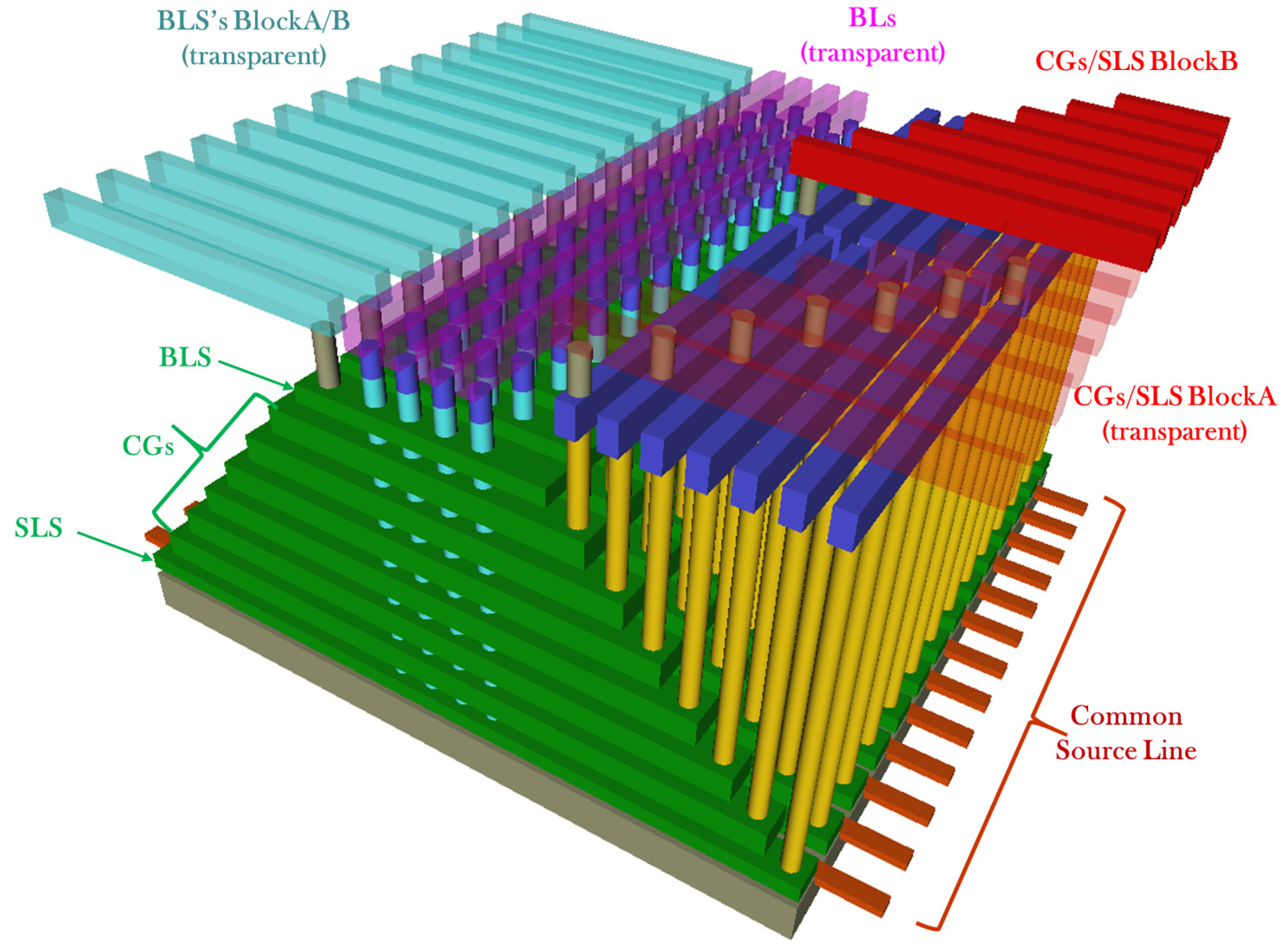
Figure 20.
Top view of an example TCAT architecture.
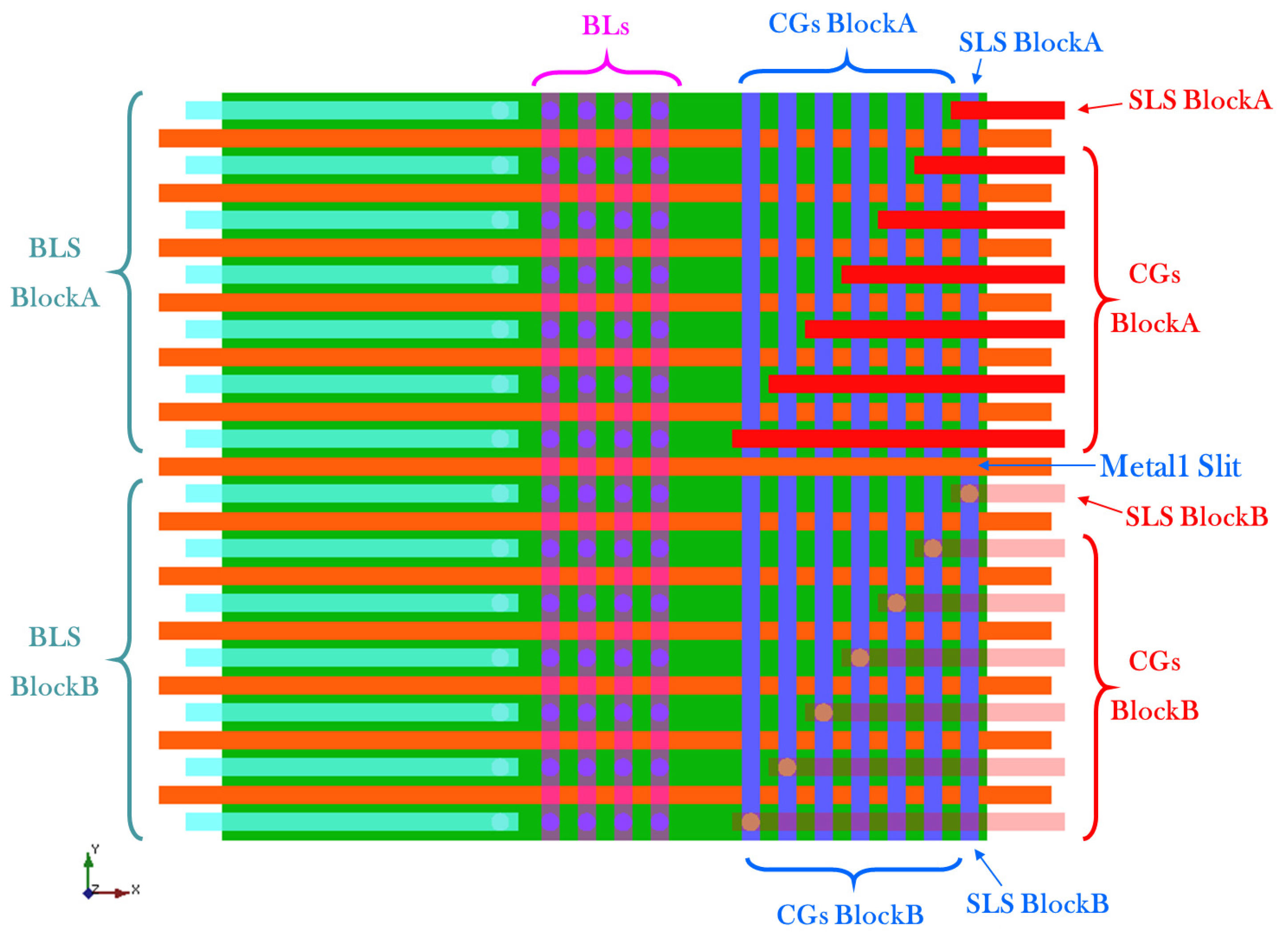
Figure 21.
(a) Trap layer structure of BiCS and (b) TCAT. Reproduced with permission from [28]. © 2010 IEEE.
Figure 21.
(a) Trap layer structure of BiCS and (b) TCAT. Reproduced with permission from [28]. © 2010 IEEE.

Figure 22.
Die micrograph of 128-Gb 2-bit/cell 3D V-NAND flash. Reproduced with permission from [31]. © 2015 IEEE.
Figure 22.
Die micrograph of 128-Gb 2-bit/cell 3D V-NAND flash. Reproduced with permission from [31]. © 2015 IEEE.
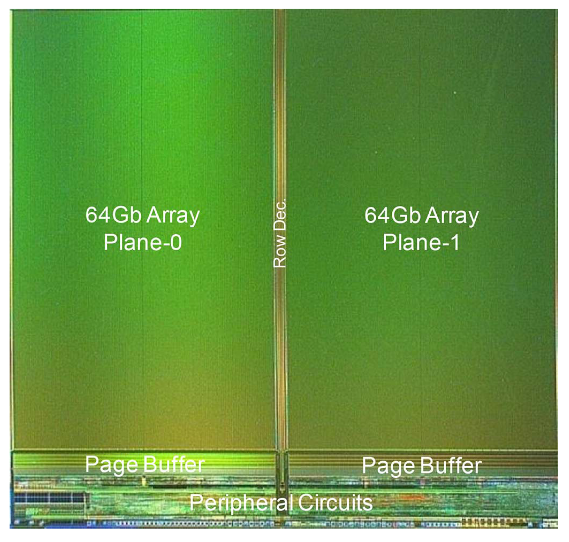
Figure 23.
First and second generations of V-NAND bit-line architecture. The page depth is extended to 16 kB from 8 kB. Reproduced with permission from [34]. © 2016 IEEE.
Figure 23.
First and second generations of V-NAND bit-line architecture. The page depth is extended to 16 kB from 8 kB. Reproduced with permission from [34]. © 2016 IEEE.

Figure 24.
Pillar etching issue when the layer number increases.


Table 1.
Bias conditions for a two-layer 3D stacked NAND Flash during read, program and erase. Adapted from [7,17]. BLn, shared bitline contact.
| Read | Program | Erase | |
|---|---|---|---|
| BLn | (0.5 V–1 V) | 0/ | Floating |
| BLS (MAT1) | Floating | ||
| Selected WL (MAT1) | 0 V | ||
| Unselected WL (MAT1) | 0 V | ||
| SLS (MAT1) | 0 V | Floating | |
| BLS (MAT2) | 0 V | 0 V | Floating |
| WL (MAT2) | Floating | Floating | Floating |
| SLS (MAT2) | 0 V | 0 V | Floating |
| SL | 0 V | Floating | |
| P-Well | 0 V | 0 V | 18 V–20 V |
© 2017 by the authors. Licensee MDPI, Basel, Switzerland. This article is an open access article distributed under the terms and conditions of the Creative Commons Attribution (CC BY) license (http://creativecommons.org/licenses/by/4.0/).
Share and Cite
MDPI and ACS Style
Micheloni, R.; Crippa, L.; Zambelli, C.; Olivo, P. Architectural and Integration Options for 3D NAND Flash Memories. Computers 2017, 6, 27. https://doi.org/10.3390/computers6030027
AMA Style
Micheloni R, Crippa L, Zambelli C, Olivo P. Architectural and Integration Options for 3D NAND Flash Memories. Computers. 2017; 6(3):27. https://doi.org/10.3390/computers6030027
Chicago/Turabian StyleMicheloni, Rino, Luca Crippa, Cristian Zambelli, and Piero Olivo. 2017. "Architectural and Integration Options for 3D NAND Flash Memories" Computers 6, no. 3: 27. https://doi.org/10.3390/computers6030027
Note that from the first issue of 2016, this journal uses article numbers instead of page numbers. See further details here.